
 Open Access Article
 This Open Access Article is licensed under a
 Creative Commons Attribution 3.0 Unported Licence
Atomistic structures of 〈0001〉 tilt grain boundaries in a textured Mg thin film†
Siyuan
Zhang
 *a,
Zhuocheng
Xie
b,
Philipp
Keuter
c,
Saba
Saood
a,
Lamya
Abdellaoui
a,
Xuyang
Zhou
a,
Niels
Cautaerts
a,
Benjamin
Breitbach
a,
Shamsa
Aliramaji
c,
Sandra
Korte-Kerzel
b,
Marcus
Hans
c,
Jochen M.
Schneider
c and
Christina
Scheu
*ac
*a,
Zhuocheng
Xie
b,
Philipp
Keuter
c,
Saba
Saood
a,
Lamya
Abdellaoui
a,
Xuyang
Zhou
a,
Niels
Cautaerts
a,
Benjamin
Breitbach
a,
Shamsa
Aliramaji
c,
Sandra
Korte-Kerzel
b,
Marcus
Hans
c,
Jochen M.
Schneider
c and
Christina
Scheu
*ac
aMax-Planck-Institut für Eisenforschung, Max-Planck-Str. 1, 40237 Düsseldorf, Germany. E-mail: siyuan.zhang@mpie.de; scheu@mpie.de
bInstitute for Physical Metallurgy and Materials Physics, RWTH Aachen University, 52074 Aachen, Germany
cMaterials Chemistry, RWTH Aachen University, Kopernikusstr. 10, 52074 Aachen, Germany
First published on 23rd November 2022
Abstract
Nanocrystalline Mg was sputter deposited onto an Ar ion etched Si {100} substrate. Despite an ∼6 nm amorphous layer found at the interface, the Mg thin film exhibits a sharp basal-plane texture enabled by surface energy minimization. The columnar grains have abundant 〈0001〉 tilt grain boundaries in between, most of which are symmetric with various misorientation angles. Up to ∼20° tilt angle, they are composed of arrays of equally-spaced edge dislocations. Ga atoms were introduced from focused ion beam milling and found to segregate at grain boundaries and preferentially decorate the dislocation cores. Most symmetric grain boundaries are type-1, whose boundary planes have smaller dihedral angles with {2![[1 with combining macron]](https://www.rsc.org/images/entities/char_0031_0304.gif) 0} rather than {100}. Atomistic simulations further demonstrate that type-2 grain boundaries, having boundary planes at smaller dihedral angles with {100}, are composed of denser dislocation arrays and hence have higher formation energy than their type-1 counterparts. The finding correlates well with the dominance of type-1 grain boundaries observed in the Mg thin film.
0} rather than {100}. Atomistic simulations further demonstrate that type-2 grain boundaries, having boundary planes at smaller dihedral angles with {100}, are composed of denser dislocation arrays and hence have higher formation energy than their type-1 counterparts. The finding correlates well with the dominance of type-1 grain boundaries observed in the Mg thin film.
1. Introduction
Most engineering materials are polycrystalline, containing countless grain boundaries (GBs) that separate single-crystalline domains of different orientations. GBs are fundamental to the mechanical and functional properties of many materials, from the Hall–Petch strengthening1 to the transport of charge carriers.2 The effects of GBs have been shown to depend on their geometric characters (GB planes, misorientation angle and axis),3 and in more general terms, the atomistic structure of the GB complexions.4,5 Thus far, most studies and theory on GBs focus on high symmetry cubic structures.6,7 In comparison, there are fewer studies on GBs in another common crystal structure, hexagonal close-packed (HCP), including Mg, Ti,8 and ZnO.9Mg is among the metallic elements with the lowest density (1.74 g cm−3) and Mg-based alloys have found increasing applications in lightweight structural systems, shielding for electronics, implants, and energy storage.10 Due to the HCP crystal structure, Mg has a limited number of slip and twin systems for plastic deformation. To enhance the strength and ductility of Mg alloys, their microstructure needs to be engineered towards refined grain size and away from special grain orientations, e.g. the basal plane texture.11 In both cases, GBs play a major role in the plasticity of Mg alloys. Thus far, twin boundaries in Mg alloys have been well characterized experimentally, along with the segregation of alloying elements.12–14 Atomistic simulations have also been employed to study the structure and energetics of GBs in Mg, including symmetric tilt GBs along the tilt axes 〈100〉,15–17 〈20〉,18,19 and 〈0001〉.20–24 Thus far, there are controversial reports on the configurations of simulated Mg 〈0001〉 tilt GBs,23,24 but a lack of experimental confirmation.
To understand the structure and properties of GBs, various ways have been explored to synthesize them for experimental studies. Deformation of Mg alloys can introduce large number of GBs, mostly twin boundaries.25 Bulk bicrystals of Mg can be grown to study single GBs over large areas.26,27 Thin film synthesis far from thermodynamic equilibrium provides a unique opportunity to study GBs that are not commonly produced by bulk materials processing. For example, textured ZnO films have been grown by pulsed laser deposition onto a quartz glass substrate.28 Bicrystalline Ti thin films were synthesized by pulsed magnetron sputtering on SrTiO3 {001}.8 Mg thin films have been already grown by thermal evaporation,29 ion beam sputtering,30 as well as direct-current and high power pulsed magnetron sputtering.31 It should be noticed that the growth temperature of Mg is limited as thermal desorption has been observed during the synthesis of Mg2Ca Laves phase thin films at temperatures above 150 °C.32 Mg–Ca solid solutions with 0.3 at% Ca were recently synthesized at a substrate temperature of 100 °C, which induced enough adatom mobility to form dense films with low impurity contents (<0.3 at% oxygen).33 In this article, we report the formation of 〈0001〉 tilt GBs in a sputtered Mg thin film, which enables a systematic survey of their structure with respect to misorientation angles.
2. Materials and methods
The Mg thin film was synthesized in a laboratory-scale high vacuum chamber applying direct-current magnetron sputtering. A circular elemental Mg target (Φ 50 mm) with a purity of 99.95% was positioned at a distance of 100 mm to the Si {100} substrate. The chamber was evacuated to a base pressure of 4 × 10⁻⁷ mbar and the substrate was heated to a temperature of ∼100 °C to ensure growth of dense films33 and avoid Mg desorption during synthesis.32 Prior to the deposition, a Si {100} substrate was plasma cleaned for 10 min applying an average power of 50 W in pulsed (frequency: 250 kHz) direct-current mode at an Ar partial pressure of 7.5 × 10⁻³ mbar. Subsequently, the Mg film was deposited for 30 min at a constant target power of 100 W onto the rotating Si substrate.X-ray diffraction (XRD) multi-axis symmetrical scan and in-plane scan were performed on the thin film using a Rigaku Smartlab diffractometer with the Cu-Kα source operated at 45 kV and 200 mA. A parallel beam was formed by the incident slits of 0.5 × 0.5 mm2 and 0.1 × 10 mm2 for the symmetrical and in-plane scans, respectively. For the in-plane pole figure measurement, both incident and receiving slits were chosen to be 1 mm.
Electron back-scattered diffraction (EBSD) was performed on a Sigma (Zeiss) scanning electron microscope (SEM). The sample was polished with Ar+ ion beam using the precision etching and coating system PECS II (Gatan). The specimen for transmission electron microscopy (TEM) was prepared on a Scios2 (Thermo Fisher) focused ion beam (FIB) system starting with Ga+ polishing at 30 kV and ending with a cleaning step at 5 kV.
Precession electron diffraction (PED) mapping was performed on a JEM2200 microscope (JEOL) operated at 200 kV. The beam size was ∼2 nm and a precession angle of 1° was used. High resolution scanning transmission electron microscopy (STEM) was performed on a Titan Themis microscope (Thermo Fisher) operated at 300 kV. The aberration-corrected STEM probe had a size less than 0.1 nm and a convergence semi-angle of 23.8 mrad. Annular bright field (ABF), low angle annular dark field (LAADF), and high angle annular dark field (HAADF) detectors for STEM image formation covered collection semi-angles of 8–16, 17–72, and 73–200 mrad, respectively. Energy dispersive X-ray spectroscopy (EDS) was performed using SuperX detectors covering ∼0.7 sr. Multivariate statistical analysis was applied to denoise the spectrum imaging dataset,34 and elemental quantification was performed using the Cliff-Lorimer method.
Atomistic simulations were performed using the open source molecular dynamics package LAMMPS.35 The interatomic interactions were modeled using the embedded atom method potential for Mg reported by Liu et al.,36 which has been widely used in studying Mg symmetric tilt GBs in the literature.15,23,24 To construct the atomic GB configurations, a Mg unit cell oriented in x-[20], y-[010], and z-[0001] was rotated along the z-axis with half of the tilt angles  using Atomsk.37 The periodicity of the supercell was restored in all directions after the rotation. Two symmetric crystals with rotation angles
  were superimposed along x, and semi-fixed boundary conditions were applied at two ends of the sample with a thickness of two times the potential cutoff (2 × 0.6 nm). The distance from the GB plane to the ends is ∼20 nm to eliminate the interaction between the GB and the semi-fixed boundaries. Periodic boundary conditions were applied along y and z. The microscopic degrees of freedom of the GB structures were explored by applying rigid body translations in all directions and atom deletion with different critical distances from 0 to 0.2 nm for the atoms at GBs.38 The dimensions of the simulation cells and the total number of atoms are listed in Table S1 (ESI†). Relaxation along the GB plane normal was performed after each translation step using the FIRE algorithm.39 Full relaxation was performed on the minimum energy configurations using the conjugate gradient and FIRE algorithms with a force tolerance of 10–7 eV nm−1. The GB energy EGB was calculated using eqn (1),
 | (1) |
3. Results and discussion
As shown in Fig. 1, the Mg thin film exhibits a sharp fiber texture with the growth direction parallel to 〈0001〉. From the multi-axis XRD scan (Fig. 1a), only the reflections parallel to the c-axis, {0002} and {0004}, show intensity. Likewise, reflections that appear in the in-plane XRD scan are all perpendicular to the c-axis. Furthermore, there is no preferential in-plane grain orientation with respect to the c-axis, as evident from the pole figures (Fig. 1b) showing isotropic diffraction intensity along the azimuth, both χ = 90° circumference for {100} and χ = 62° circle for {101}.
 | ||
| Fig. 1 (a) Multi-axis XRD 2θ scan overlapped with in-plane XRD 2θ scan with labelled Mg reflections (Mg is not specified in the label) and Si {400}; (b) pole figures of {100}, {0002}, and {101} reflections. | ||
As there is no preferred in-plane orientation at the scale of the wafer, we further investigate the grain distribution on the micrometer scale. As shown in Fig. 2a and b, most grains are equiaxed in-plane and aligned with the normal direction along 〈0001〉. The in-plane orientation ranges along the arc between 〈100〉 (blue) and 〈20〉 (green). With the c-plane fiber texture, the biggest misorientation between two grains is 30° between 〈100〉 and 〈20〉, and the GBs with misorientations above 5° are highlighted in Fig. 2b. As shown in Fig. 2c, the grain size follows a log–normal distribution, with the median value at ∼0.6 μm. The misorientation angles between grains are uniform between 3° and 30° (Fig. 2d), indicating that the grains were nucleated randomly in the in-plane direction.
 | ||
| Fig. 2 Plan view EBSD of Mg: (a) orientation map along the growth direction, (b) orientation map along the horizontal in-plane direction with GBs highlighted in black (inset: color scale for (a) and (b)), (c) grain size distribution, (d) distribution of GB misorientation. | ||
While a strong fiber texture has been observed for the thin film growth onto the plasma cleaned Si {100} substrate, large globular grains were found for a film grown onto the as-delivered Si {100} substrate (not shown). Thus, the plasma cleaning of the substrate has a vital role in the fiber texture obtained here. To study the origin of the fiber texture, the interface between Mg and Si is characterized down to the atomic scale. As shown in Fig. 3a, the columnar grains have straight boundaries along the entire film thickness of 2 μm. The orientation relationship Mg (0002)//Si (100) is observed in all grains, in agreement with the observed basal-plane fiber texture. As shown by the plan view EBSD characterization (Fig. 2b), there is a degree of freedom in the in-plane rotation, with Si [011] being parallel to all possible directions within the Mg basal plane, e.g. Mg [20] (Fig. 3b).
 | ||
| Fig. 3 Cross-sectional (a) ABF-STEM micrograph of columnar Mg grains, (b) atomically-resolved HAADF-STEM micrograph of the Si substrate and the selected Mg grain along [20], and (c) high resolution ABF-STEM micrograph of the interface between Mg and Si; (d) EDS elemental maps of the area imaged in (c) and the integrated line profile of the molar composition. | ||
Despite the sharp texture, the interface between Mg and Si was found to be amorphous. As shown in Fig. 3c, there is an ∼6 nm amorphous layer between crystalline Mg and Si. As shown by the EDS characterization (Fig. 3d), Ar and O are enriched at the interface between Mg and the amorphous layer. After the Ar plasma was applied to etch the Si surface, the deposition of crystalline Mg was initiated. The ∼1 nm thickness of Ar enrichment agrees well with the surface roughness of Si {100} after Ar plasma etching.42 In the same report, Ar plasma etching was shown to cause the formation of a 5.5 nm amorphous layer at the Si {100} surface, which is in line with the thickness of the amorphous layer observed here. During the growth process, it is likely that Mg atoms diffused into the amorphous Si layer leading to the observed composition, while further Mg diffusion into the crystalline Si lattice did not occur.
A necessary requirement for epitaxial growth of thin films is the presence of crystalline interfaces. For example, the interface between the molecular beam epitaxy-grown GaN thin film and the Ge {111} substrate is crystalline, and a reconstruction at the interface was found to be favorable for the low energy growth of GaN along 〈0001〉.43 However, in a similar system, metalorganic vapor phase epitaxy-grown AlN on a Si {111} substrate, a nanometer-thick amorphous layer was found at the interface.44 Nevertheless, the film exhibited an epitaxial relationship with the substrate, AlN along 〈0001〉, so that the interface was believed to have been crystalline in the beginning. The amorphous SiNx layer in between AlN and Si was hence reasoned to have formed by the diffusion of N into Si during the subsequent AlN growth at high temperatures.44 Unlike the epitaxial growth of the aforementioned nitride films on Si and Ge, the deposition of Mg on Si {100} exhibits a fiber texture, which has also been observed in the growth of Ti8 and many other thin films.45,46 The basal plane {0002} has the smallest surface energy among all Mg surface terminations,47 which provides the driving force for the evolution of the strong basal-plane texture in the as-deposited Mg thin film.
The sharp basal-plane texture provides opportunities to study the structure of 〈0001〉 tilt GBs based on significant statistics for the whole range of misorientation angles. A plan view TEM lamella was taken from the middle part along the film thickness to avoid the amorphous layer at the interface or the native oxide on the surface, and thinned down to ∼100 nm by focused Ga+ ion milling. The orientation maps (Fig. 4a) obtained from PED (Fig. 4b) confirm the basal plane texture as shown in Fig. 2. Most GBs appear as straight lines that extend their second dimension into the film thickness.
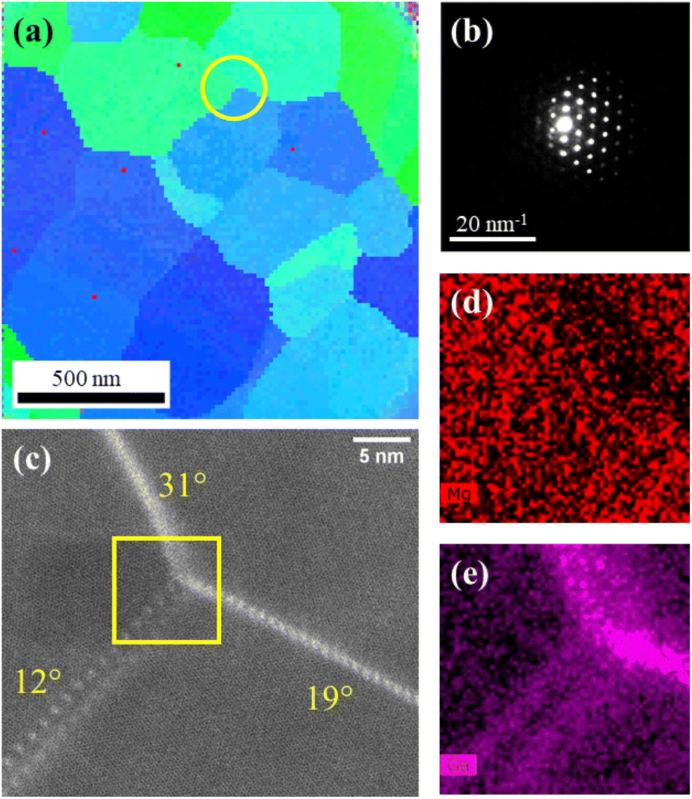 | ||
| Fig. 4 Plan view (a) in-plane orientation map (color scale the same as Fig. 2b) derived from PED, (b) an example PED pattern showing a grain oriented very close to the Mg[0001] zone axis, (c) HAADF-STEM micrographs of a triple junction, and the EDS map of integrated (d) Mg and (e) Ga counts in the highlighted area. | ||
A triple junction from the highlighted area in Fig. 4a is shown in Fig. 4c. The bright contrast is obvious at each GB, some of which is interrupted with periodicity. The bright HAADF contrast indicates more strongly scattering elements (higher atomic number). Indeed it is confirmed from the EDS maps (Fig. 4d and e) that the GB area is enriched in Ga, with a corresponding depletion of Mg. The only source of Ga was Ga+ ion milling during the FIB preparation. The ions were implanted homogeneously throughout the sample surface, but later found to segregate at the GBs. Segregation of Ga to GBs in Al is a well-documented phenomenon, causing the embrittlement of Al alloys.48 It was also shown that with Ga+ FIB preparation, Ga atoms preferentially segregate to the GBs of Al samples.49 Segregation of Ga to Mg GBs has also been recently revealed by atom probe tomography.31
We make use of segregated Ga atoms as tracers to investigate 〈0001〉 tilt GBs with various misorientations. As shown in the high resolution micrographs in Fig. 5, the GBs with smaller misorientation angles (<20°) are composed of arrays of dislocations (a–c). Like the interrupted bright contrast in Fig. 4c, here the dislocation cores are decorated by Ga atoms. By the Burgers circuit analysis, their Burgers vector (red arrows in Fig. 5a–c) is determined as  . Their line direction is along the tilt axis 〈0001〉, which is perpendicular to the glissile edge dislocation lines responsible for the basal plane slip. It is also noteworthy that the dislocations are very well aligned along a straight GB plane, with nearly identical spacing between them, at 1.95 nm (9°), 1.51 nm (12°), and 1.07 nm (17°). The observed misorientation angle θ and the spacing between dislocations D agree very well with Frank's formula, eqn (2),
 | (2) |
 in Mg is |b| = 0.32 nm.
 | ||
Fig. 5 HAADF-STEM micrographs of GBs with misorientation angles of (a) 9°, (b) 12°, (c) 17°, and (d) 30°. The Burgers circuits were completed around dislocation cores to confirm their Burgers vector  . Scale bars are 2 nm. . Scale bars are 2 nm. | ||
At higher tilt angles, the dislocation cores start to overlap and the entire length of GBs is decorated by Ga, as shown in Fig. 5d. High angle GBs are commonly referred to as coincidence site lattice (CSL)50 GBs with the closest misorientation angle. A list of CSL 〈0001〉 symmetric tilt GBs with low index Σ are tabulated in Table 1. For each Σ value, there is a pair of tilt angles θ1 and θ2 (θ1 + θ2 = 60°) that correspond to different GB planes, while they can be mapped to the same misorientation angle in the range between 0° and 30° (see Fig. 4b). As introduced by Inoue et al.,9 the extended range of tilt angles (0°–60°) can be classified by whether both atoms in the HCP lattice overlap with the CSL lattice  or only one of the two atoms overlaps
  . It is also noteworthy that a Σ value can correspond to more than one pair of tilt angles, e.g. Σ91 in Table 1, although it is rarely encountered in the literature, as the index is relatively high. To identify a GB without ambiguity, referencing the GB plane (or in the case of asymmetric GBs, the GB planes in the indices of both grains) along with the tilt axis remains the recommendation.
| Σ |
![[capital Sigma, Greek, macron]](https://www.rsc.org/images/entities/i_char_e1f5.gif)
|
Tilt angle (°) | GB plane |
|---|---|---|---|
| 1 | 1 | 0 | {2, , , 0} |
| 1 | 2 | 60 | {1, 0, , 0} |
| 7 | 7 | 38.21 | {5, , ![[4 with combining macron]](https://www.rsc.org/images/entities/char_0034_0304.gif) , 0} , 0} |
| 7 | 14 | 21.79 | {3, , ![[2 with combining macron]](https://www.rsc.org/images/entities/char_0032_0304.gif) , 0} , 0} |
| 13 | 13 | 27.80 | {7, , ![[5 with combining macron]](https://www.rsc.org/images/entities/char_0035_0304.gif) , 0} , 0} |
| 13 | 26 | 32.20 | {4, , ![[3 with combining macron]](https://www.rsc.org/images/entities/char_0033_0304.gif) , 0} , 0} |
| 19 | 19 | 46.83 | {8, , ![[7 with combining macron]](https://www.rsc.org/images/entities/char_0037_0304.gif) , 0} , 0} |
| 19 | 38 | 13.17 | {5, , , 0} |
| 31 | 31 | 17.90 | {11, , , 0} |
| 31 | 62 | 42.10 | {6, , , 0} |
| 37 | 37 | 50.57 | {11, , ![[0 with combining macron]](https://www.rsc.org/images/entities/char_0030_0304.gif) , 0} , 0} |
| 37 | 74 | 9.43 | {7, , , 0} |
| 43 | 43 | 15.18 | {13, , ![[8 with combining macron]](https://www.rsc.org/images/entities/char_0038_0304.gif) , 0} , 0} |
| 43 | 86 | 44.82 | {7, , ![[6 with combining macron]](https://www.rsc.org/images/entities/char_0036_0304.gif) , 0} , 0} |
| 49 | 49 | 43.57 | {13, , , 0} |
| 49 | 98 | 16.43 | {8, , , 0} |
| 61 | 61 | 52.66 | {14, , , 0} |
| 61 | 122 | 7.34 | {9, , , 0} |
| 67 | 67 | 24.43 | {16, , , 0} |
| 67 | 134 | 35.57 | {9, , , 0} |
| 73 | 73 | 11.64 | {17, , , 0} |
| 73 | 146 | 48.36 | {9, , , 0} |
| 79 | 79 | 33.99 | {17, , , 0} |
| 79 | 158 | 26.01 | {10, , , 0} |
| 91 | 91 | 10.42 | {19, , , 0} |
| 91 | 182 | 49.58 | {10, , ![[9 with combining macron]](https://www.rsc.org/images/entities/char_0039_0304.gif) , 0} , 0} |
| 91 | 91 | 53.99 | {17, , , 0} |
| 91 | 182 | 6.01 | {11, , , 0} |
| 97 | 97 | 30.59 | {19, , , 0} |
| 97 | 194 | 29.41 | {11, , , 0} |
Another way to classify the 〈0001〉 symmetric tilt GBs is by the tilt angle, defined as twice the dihedral angle between the GB plane and {20}. Note that a tilt ϕ from {20} towards {100} is equivalent to a tilt 30° − ϕ from {100} towards {20}. Therefore, twice the dihedral angle maps any symmetric tilt angle θ with respect to {20} onto 60° − θ with reference to {100}. The 〈0001〉 symmetric tilt GBs can be hence classified by their GB planes closer to {20} (θ < 30°) or {100} (θ > 30°), which are respectively referred to as type-1 or type-2 by Barrett et al.24 As an example, Fig. 6a shows a GB of 11° misorientation with different sections of GB planes, including two symmetric sections. According to the analysis in Fig. 6b, the normal direction of the symmetric GB plane in yellow (or orange) opens up the same dihedral angles with respect to the {20} planes of both grains that sum up to 11° (or 49°) tilt angle.
 | ||
| Fig. 6 (a) HAADF-STEM micrograph of a 〈0001〉 tilt GB with 11° misorientation angle including two symmetric sections of tilt angles 11° and 49°. (b) Fast Fourier transform of Fig. 6a shows {100} (labelled with the inner dotted arc) and {20} (outer dotted arc) reflections. Traces of both symmetric planes are plotted (yellow: 11°, orange: 49°) with their normal directions as arrows of corresponding colors. The pairs of {20} reflections symmetric to the yellow and orange arrows have respective tilt angles of 11° (type-1) and 49° (type-2). (c) The population of type-1 and type-2 GBs observed in experiments. | ||
It is noteworthy that we predominantly observed type-1 GBs (θ < 30°) from the textured thin film, whose GB planes are closer to {20}. The histogram in Fig. 6c highlights the preference of type-1 GBs over their type-2 counterparts with 60° − θ tilt angles. As discussed above, type-1 GBs with smaller tilt angles (<20°) with respect to {20} are accommodated by arrays of dislocations with  . Like in Fig. 5a–c, the Ga segregation pattern of the 11° yellow symmetric section (type-1) in Fig. 6a is a straight line with equal spacing. On the other hand, the Ga segregation pattern of the 49° orange symmetric section (type-2) is more serrated.
Atomistic simulations were performed on four pairs of CSL 〈0001〉 symmetric tilt GBs, Σ61, Σ37, Σ73, and Σ31, including both GB planes corresponding to type-1 and type-2. As shown in Fig. 7a, all calculated type-2 GBs have higher formation energies than their type-1 counterparts, which can explain the dominant population of type-1 GBs observed in experiments (Fig. 6c). Moreover, the GB energy fits nicely to the formula for low angle GBs, eqn (3),51
| EGB(θ) = E0θ(A − ln(θ)) | (3) |
 | ||
Fig. 7 (a) Formation energy of four pairs of type-1 and type-2 CSL GBs evaluated from atomistic simulations. The energy curves are fitted with eqn (3). Atomic configurations of simulated (b) Σ37 type-1 (9.43°) and (c) Σ37 type-2 (50.57°) GBs with color codes that highlight the stress field. Dislocation lines parallel to the viewing direction are colored in green and the overlaid Burgers vectors  are indicated using red arrows. are indicated using red arrows. | ||
To understand the origin of higher energy type-2 GBs, their atomic arrangements are plotted in Fig. 7b, c and Fig. S1 in the ESI.† From the simulations, the two Σ37 GBs correspond closely to those observed in STEM (Fig. 6a), with {7, , , 0} (9.43°, type-1) and {11, , , 0} (50.57°, type-2) GB planes (Table 1). As shown in Fig. 7b, the dislocation arrays with  reproduce the experimental observations in type-1 GBs. In comparison, two sets of dislocation arrays with
  and
and  are observed in the type-2 GB shown in Fig. 7c, summing up to b1 + b2 = 〈100〉. Such an arrangement of dislocation arrays has been reported for type-2 GBs in ZnO, another crystal with a HCP structure.9 Like for type-1 GBs, we can apply Frank's formula to calculate the dislocation spacing 2D between arrays of b1 + b2 dislocations (for Mg,
  ), replacing θ > 30° to the small angles 60° − θ in eqn (4),
 | (4) |
 . This is because all dislocations constituting type-1 GBs (Fig. 7b) have Burgers vectors aligned perpendicular to the GB plane and hence fully contribute to the tilt angle. On the other hand, the Burgers vectors b1 and b2 forming type-2 GBs have components parallel to the GB plane that cancel each other out. As a result, although b1 and b2 sum up to make symmetric tilt boundaries, a higher density than that of the type-1 counterpart is required to constitute the same misorientation.
Our combined experimental and simulation results have shown that low angle type-1 (θ < 20°) and type-2 (40° < θ < 60°) GBs are composed of their respective dislocation arrays. The higher dislocation density of type-2 GBs than that of their type-1 counterparts leads to their higher formation energy, and hence rarer occurrences. We further note that similar atomic configurations of type-1 and type-2 GBs have been characterized for ZnO,9 so that our findings with regard to the energetics and structure of type-1 and type-2 〈0001〉 symmetric tilt GBs should be applicable to HCP crystals in general. Simulation reports on 〈0001〉 symmetric tilt GBs in HCP Ti have demonstrated a higher energy of type-2 GBs.20,52 Nevertheless, there is a lack of simulation for θ > 45°, where the dislocations become less dense as θ approaches 60°. Some simulation studies on 〈0001〉 symmetric tilt GBs in Mg show a similar GB energy in type-1 and type-2 GBs.23,24 It is noteworthy that the report from Liu and Wang23 uses a different definition of tilt angle θ′, which can be translated to θ in this article (the same definition adopted from Barret et al.24) as θ = 60° − 2θ′. As such, θ = 0° and 60° (θ′ = 30° and 0°, respectively) should correspond to a perfect crystal misorientation. Liu and Wang nevertheless constructed a planar defect into their θ′ = 30° GB, resulting in a non-zero GB energy,23 making it impossible to draw a direct comparison between their type-1 and type-2 GBs.
4. Conclusions
We have demonstrated the growth of a sharply basal-plane textured Mg thin film, which was sputter deposited on an Ar ion etched Si {100} substrate. Despite an ∼6 nm amorphous layer present at the interface, the low surface energy of Mg {0002} provided the driving force for the strong basal plane texture. The columnar Mg grains are oriented along 〈0001〉 and form many tilt GBs between them. With a uniform distribution of misorientation angles, a variety of low to high angle GBs can be studied. Ga atoms introduced by FIB preparation were found to segregate at the GBs and facilitate the identification of GBs. We observed predominantly symmetric tilt GBs with GB planes closer to {20} (type-1) rather than to {100} (type-2). For smaller tilt angles of type-1 GBs (θ < 20°), they are composed of arrays of equally-spaced edge dislocations  , with Ga atoms segregated to the dislocation cores. At larger misorientation angles, Ga segregation can cover the entire GB. For type-2 GBs with small misorientation (40° < θ < 60°), they are composed of two arrays of edge dislocations with
  and
and  , summing up to 〈100〉. Dislocations constituting type-2 〈0001〉 symmetric tilt GBs have higher density than their type-1 counterparts. Consequently, the formation energy of type-2 GBs is also higher, which explains the dominant population of type-1 GBs observed in experiments. The preference of type-1 GB planes may be applicable to other HCP crystals. The implications for materials properties and microstructural evolution can be subjects for future investigations.
Author contributions
All authors contributed to the review and editing of the manuscript. In addition, Siyuan Zhang: conceptualization, investigation, formal analysis, writing – original draft; Zhuocheng Xie: investigation, formal analysis; Philipp Keuter: investigation; Saba Saood: investigation; Lamya Abdellaoui: investigation; Xuyang Zhou: formal analysis; Niels Cautaerts: investigation; Benjamin Breitbach: investigation; Shamsa Aliramaji: investigation; Sandra Korte-Kerzel: funding acquisition; Marcus Hans: investigation, funding acquisition; Jochen M. Schneider: funding acquisition; Christina Scheu: conceptualization, funding acquisition.Conflicts of interest
There are no conflicts to declare.Acknowledgements
This work was supported by the Deutsche Forschungsgemeinschaft (DFG) within the Collaborative Research Center SFB 1394 “Structural and Chemical Atomic Complexity—From Defect Phase Diagrams to Materials Properties” (Project ID 409476157) including the project groups A02, B01, B02, B03, and C02. Simulations were performed with computing resources granted by RWTH Aachen University under project (p0020267). Z.X. acknowledges the financial support by the DFG (Grant Nr. XI265/1-1). Open Access funding provided by the Max Planck Society.References
- E. O. Hall, Proc. Phys. Soc., London, Sect. B, 1951, 64, 747–753 CrossRef.
- D. P. Joshi and D. P. Bhatt, IEEE Trans. Electron Devices, 1990, 37, 237–249 CrossRef CAS.
- C. M. Barr, S. M. Foiles, M. Alkayyali, Y. Mahmood, P. M. Price, D. P. Adams, B. L. Boyce, F. Abdeljawad and K. Hattar, Nanoscale, 2021, 13, 3552–3563 RSC.
- P. R. Cantwell, M. Tang, S. J. Dillon, J. Luo, G. S. Rohrer and M. P. Harmer, Acta Mater., 2014, 62, 1–48 CrossRef CAS.
- T. Meiners, T. Frolov, R. E. Rudd, G. Dehm and C. H. Liebscher, Nature, 2020, 579, 375–378 CrossRef CAS PubMed.
- S. Ranganathan, Acta Cryst., 1966, 21, 197–199 CrossRef CAS.
- H. Zheng, X. G. Li, R. Tran, C. Chen, M. Horton, D. Winston, K. A. Persson and S. P. Ong, Acta Mater., 2020, 186, 40–49 CrossRef CAS.
- V. Devulapalli, M. Hans, P. T. Sukumar, J. M. Schneider, G. Dehm and C. H. Liebscher, Acta Mater., 2022, 238, 118180 CrossRef CAS.
- K. Inoue, J. Y. Roh, K. Kawahara, M. Saito, M. Kotani and Y. Ikuhara, Acta Mater., 2021, 212, 116864 CrossRef CAS.
- T. M. Pollock, Science, 2010, 328, 986–987 CrossRef CAS PubMed.
- R. Gehrmann, M. M. Frommert and G. Gottstein, J. Mater. Sci. Eng. A, 2005, 395, 338–349 CrossRef.
- J. F. Nie, Y. M. Zhu, J. Z. Liu and X. Y. Fang, Science, 2013, 340, 957–960 CrossRef CAS PubMed.
- X. Zhao, H. Chen, N. Wilson, Q. Liu and J.-F. Nie, Nat. Commun., 2019, 10, 3243 CrossRef PubMed.
- X. F. Chen, L. R. Xiao, Z. G. Ding, W. Liu, Y. T. Zhu and X. L. Wu, Scr. Mater., 2020, 178, 193–197 CrossRef CAS.
- J. Wang and I. J. Beyerlein, Modell. Simul. Mater. Sci. Eng., 2012, 20, 0–22 Search PubMed.
- C. Ni, H. Ding, M. Asta and X. Jin, Scr. Mater., 2015, 109, 94–99 CrossRef CAS.
- A. Ostapovets and A. D. Sheikh-Ali, Philos. Mag., 2018, 98, 3235–3246 CrossRef CAS.
- C. Xu, L. Yuan, R. Shivpuri, D. Shan and B. Guo, Modell. Simul. Mater. Sci. Eng., 2019, 27, 035004 CrossRef CAS.
- Z. Xu, S. Tanaka and M. Kohyama, Modell. Simul. Mater. Sci. Eng., 2021, 29, 085010 CrossRef CAS.
- Y. C. Wang and H. Q. Ye, Philos. Mag. A, 1997, 75, 261–272 CAS.
- H. A. Khater, A. Serra, R. C. Pond and J. P. Hirth, Acta Mater., 2012, 60, 2007–2020 CrossRef CAS.
- L. Huber, J. Rottler and M. Militzer, Acta Mater., 2014, 80, 194–204 CrossRef CAS.
- X. Liu and J. Wang, Sci. Rep., 2016, 6, 21393 CrossRef CAS PubMed.
- C. D. Barrett, A. Imandoust, A. L. Oppedal, K. Inal, M. A. Tschopp and H. El Kadiri, Acta Mater., 2017, 128, 270–283 CrossRef CAS.
- Y. Liu, P. Z. Tang, M. Y. Gong, R. J. McCabe, J. Wang and C. N. Tomé, Nat. Commun., 2019, 10, 1–7 CrossRef PubMed.
- K. D. Molodov, T. Al-Samman and D. A. Molodov, Acta Mater., 2017, 124, 397–409 CrossRef CAS.
- H. Yang, B. Jiang, J. He, Z. Jiang, J. Zhang and F. Pan, J. Alloys Compd., 2017, 725, 1282–1287 CrossRef CAS.
- F. Oba, H. Ohta, Y. Sato, H. Hosono, T. Yamamoto and Y. Ikuhara, Phys. Rev. B: Condens. Matter Mater. Phys., 2004, 70, 125415 CrossRef.
- J. Karst, M. Hentschel, F. Sterl, H. Linnenbank, M. Ubl and H. Giessen, Opt. Mater. Express, 2020, 10, 1346 CrossRef CAS.
- E. Hadjixenophontos, M. Roussel, T. Sato, A. Weigel, P. Stender, S. Orimo and G. Schmitz, Int. J. Hydrogen Energy, 2017, 42, 22411–22416 CrossRef CAS.
- F. Moens, I. C. Schramm, S. Konstantinidis and D. Depla, Thin Solid Films, 2019, 689, 137501 CrossRef CAS.
- P. Keuter, S. K. Aghda, D. Music, P. Kümmerl and J. M. Schneider, Materials, 2019, 12, 3026 CrossRef CAS.
- M. Hans, P. Keuter, A. Saksena, J. A. Sälker, M. Momma, H. Springer, J. Nowak, D. Zander, D. Primetzhofer and J. M. Schneider, Sci. Rep., 2021, 11, 17454 CrossRef CAS PubMed.
- S. Zhang and C. Scheu, Microscopy, 2018, 67, i133–i141 CrossRef CAS PubMed.
- S. Plimpton, J. Comput. Phys., 1995, 117, 1–19 CrossRef CAS.
- X. Y. Liu, J. B. Adams, F. Ercolessi and J. A. Moriarty, Modell. Simul. Mater. Sci. Eng., 1996, 4, 293–303 CrossRef CAS.
- P. Hirel, Comput. Phys. Commun., 2015, 197, 212–219 CrossRef CAS.
- M. A. Tschopp and D. L. McDowell, Philos. Mag., 2007, 87, 3147–3173 CrossRef CAS.
- J. Guénolé, W. G. Nöhring, A. Vaid, F. Houllé, Z. Xie, A. Prakash and E. Bitzek, Comput. Mater. Sci., 2020, 175, 109584 CrossRef.
- A. Stukowski, Modell. Simul. Mater. Sci. Eng., 2010, 18, 015012 CrossRef.
- A. Stukowski, V. V. Bulatov and A. Arsenlis, Modell. Simul. Mater. Sci. Eng., 2012, 20, 085007 CrossRef.
- M. E. Day, M. Delfino, W. Tsai, A. Bivas and K. N. Ritz, J. Appl. Phys., 1993, 74, 5217–5224 CrossRef CAS.
- S. Zhang, Y. Zhang, Y. Cui, C. Freysoldt, J. Neugebauer, R. Lieten, J. Barnard and C. Humphreys, Phys. Rev. Lett., 2013, 111, 256101 CrossRef PubMed.
- G. Radtke, M. Couillard, G. A. Botton, D. Zhu and C. J. Humphreys, Appl. Phys. Lett., 2012, 100, 011910 CrossRef.
- T. Takahashi, R. Iskandar, F. Munnik, D. Music, J. Mayer and J. M. Schneider, J. Alloys Compd., 2012, 540, 75–80 CrossRef CAS.
- M. to Baben, M. Hans, D. Primetzhofer, S. Evertz, H. Ruess and J. M. Schneider, Mater. Res. Lett., 2017, 5, 158–169 CrossRef CAS.
- J. J. Tang, X. B. Yang, L. Ouyang, M. Zhu and Y. J. Zhao, J. Phys. D: Appl. Phys., 2014, 47, 115305 CrossRef.
- S. Schmidt, W. Sigle, W. Gust and M. Rühle, Z. Metallkd., 2002, 93, 428–431 CrossRef CAS.
- X. Zhong, C. A. Wade, P. J. Withers, X. Zhou, C. Cai, S. J. Haigh and M. G. Burke, J. Microsc., 2021, 282, 101–112 CrossRef CAS PubMed.
- H. Grimmer and D. H. Warrington, Acta Crystallogr., Sect. A: Found. Crystallogr., 1987, 43, 232–243 CrossRef.
- W. T. Read and W. Shockley, Phys. Rev., 1950, 78, 275–289 CrossRef CAS.
- Z. Zheng, D. S. Balint and F. P. Dunne, Acta Mater., 2017, 127, 43–53 CrossRef CAS.
Footnote |
| † Electronic supplementary information (ESI) available: Details on the atomistic simulations and atomic configurations of GBs. See DOI: https://doi.org/10.1039/d2nr05505h |
| This journal is © The Royal Society of Chemistry 2022 |