
 Open Access Article
 This Open Access Article is licensed under a
 Creative Commons Attribution 3.0 Unported Licence
3D-structured mesoporous silica memristors for neuromorphic switching and reservoir computing†
Ayoub H.
Jaafar
ab,
Li
Shao
c,
Peng
Dai
a,
Tongjun
Zhang
a,
Yisong
Han
d,
Richard
Beanland
d,
Neil T.
Kemp
b,
Philip N.
Bartlett
 c,
Andrew L.
Hector
*c and
Ruomeng
Huang
*a
c,
Andrew L.
Hector
*c and
Ruomeng
Huang
*a
aSchool of Electronics and Computer Science, University of Southampton, Southampton, SO17 1BJ, UK. E-mail: r.huang@soton.ac.uk
bSchool of Physics and Astronomy, University of Nottingham, Nottingham, NG7 2RD, UK
cSchool of Chemistry, University of Southampton, Southampton, SO17 1BJ, UK. E-mail: a.l.hector@soton.ac.uk
dDepartment of Physics, University of Warwick, Coventry, CV4 7AL, UK
First published on 10th November 2022
Abstract
Memristors are emerging as promising candidates for practical application in reservoir computing systems that are capable of temporal information processing. Here, we experimentally implement a physical reservoir computing system using resistive memristors based on three-dimensional (3D)-structured mesoporous silica (mSiO2) thin films fabricated by a low cost, fast and vacuum-free sol–gel technique. The in situ learning capability and a classification accuracy of 100% on a standard machine learning dataset are experimentally demonstrated. The volatile (temporal) resistive switching in diffusive memristors arises from the formation and subsequent spontaneous rupture of conductive filaments via diffusion of Ag species within the 3D-structured nanopores of the mSiO2 thin film. Besides volatile switching, the devices also exhibit a bipolar non-volatile resistive switching behavior when the devices are operated at a higher compliance current level. The implementation of mSiO2 thin films opens the route to fabricate a simple and low cost dynamic memristor with a temporal information process functionality, which is essential for neuromorphic computing applications.
1. Introduction
Neuromorphic systems that are inspired by the structure and operation of biological neural networks are considered to be the hardware solution to tackle the information transfer bottleneck that is inherent in the conventional von Neumann computing architectures.1–3 Two-terminal memristors exhibit reversible resistance modulation through changes in their internal material composition under external stimuli and have received enormous attention in the application of neuromorphic computing systems to emulate the analogue switching and learning properties of biological synapses.4–8 In general, resistive switching in memristors is categorized into two types: non-volatile (non-temporal or long-term plasticity (LTP)) and volatile (temporal or short-term plasticity (STP)).5 Non-volatile resistive switching is characterized by the permanently stored resistance state after stimulation and has been widely used in constructing feedforward neural networks (FNNs) for static (non-temporal) data processing.9,10 Volatile resistive switching, on the other hand, features temporally stored resistance states that can represent temporal information of the input signals. Such switching dynamics can therefore be used to directly process temporal data in a bio-faithful fashion in recurrent neural networks (RNNs).11 Compared with FNNs where the input–output mapping is stateless, RNNs can sustain reverberations of activations even after the input layer becomes inactive.12 This means that the output of the RNN model depends not only on the current input, but also on the current state of the network. This unique temporal dynamic behaviour is particularly attractive for applications such as speech recognition, classification and time series forecasting.13A reservoir computing (RC) system is a framework derived from RNNs and is a suitable candidate for temporal and sequential data processing.11,14 It normally consists of massive nonlinear elements that transform the input pulses’ spatiotemporal patterns in a high-dimensional space within the reservoir, which are then analyzed by readout function using a simple learning algorithm.15 In the reservoir network, only the node states connecting the reservoir layer and the output layer are required to be read out through linear weighted sums for recognition. As a result, the reservoir itself does not need to be trained but only the output connections with linear weights do, which makes the training process simple, fast, and energy-efficient.11,16–18 The implementation of physical reservoir computing requires a physical system to act as a reservoir to produce a nonlinear and high-dimensional response to the external stimuli. To qualify as a suitable physical reservoir, the response of the system must have many degrees of freedom, and ideally the system should also allow some control parameters that may be tuned to change the response of the reservoir.12
To process temporal information, the reservoir states need to be determined by both present and past inputs within a certain period of time. Physical memristors featuring the properties of STP and nonlinear dynamics are therefore desirable for the implementation of RC systems.11 Compared with the conventional memory devices (e.g. DRAM), a filamentary-based memristor offers much higher complexity as its temporal dynamics originated from the random formation and spontaneous dissolution of the conductive filament(s) in response to external stimuli. In a resistive memristor, the STP behavior normally relies on the spontaneous dissolution of the conductive filament(s) after the withdrawal of stimuli.5 A faster dissolution can therefore be extremely advantageous to enable a faster processing time and lower power consumption.19 However, this significantly depends on the ion transfer dynamics in the dielectric layer. Different dielectric materials compositions, qualities and morphologies can all contribute to the different ionic dynamics, resulting in diverse synaptic properties.6 Realizing STP behavior normally requires careful tuning of the external programmed voltage pulse. Several memristor devices have since been applied in implementing physical RC systems using dielectric materials such as WOx,13,17 Ta2O5,20 TiOx,16 HfO2,21 and lead-free Cs3Sb2Br9 perovskite19 as the active electrolyte switching materials to enable STP behavior.
Mesoporous nanocomposite materials feature strongly in the field of energy storage due to their high surface to volume ratio as well as fast electron transport and reduced resistance of charge transfer.22 Such advantages could also be capitalized in neuromorphic switching to achieve the desired synaptic function. Through the introduction of porous structures into the electrolyte layer of a memristor, the ionic dynamics and the growth of conductive filaments can be regulated through control over the pore geometries.23,24 Several mesoporous film-based memristors have been reported to demonstrate resistive and synaptic switching behaviors.25–29 Choi et al. reported the analog and multilevel conductance with a low variation using a TiO2-based memristor with pre-defined one-dimensional (1D) pore structures.30 Li et al. reported the mediation of the STP behavior from a memristor based on oriented 1D mesoporous SiO2 (mSiO2) thin films with a thermally evaporated Ag2S layer.31 They discovered that the existence of mesopores facilitates the growth and dissolution of Ag filaments due to reduced atom strain energy, leading to a shorter relaxation time compared with amorphous silica electrolytes. Nevertheless, further reduction of relaxation is limited by the grain boundaries in the 1D pore structure which serve as the energy barrier for diffusion.32 Mesoporous structures with higher dimensions, therefore, possess great potential to further improve ion diffusion through multiple drift and diffusion pathways, enabling nonlinear and high-dimensional responses to external stimuli requested for a physical reservoir. However, a physical RC system based on memristors with three-dimensional (3D) mesoporous structures, to the best of our knowledge, has never been reported.
In this work, we demonstrate the implementation of a physical RC system using a 3D-structured, highly ordered mSiO2 based memristor that is fabricated via a vacuum-free, low cost and fast sol–gel solution processing technique. The memristor exhibits both volatile and non-volatile resistive switching behaviors that are tunable by controlling the applied compliance current (CC). The fast mobility and diffusivity of Ag+ ion species migrating within the 3D porous structures enable the demonstration of the STP behavior and temporal dynamics. A RC system based on this mSiO2 diffusive memristor has been experimentally demonstrated to perform a pattern recognition task with the 3D-structured mSiO2 layer serving as a reservoir matrix for the system. This work opens the route for simple and low cost memristor devices for building neuromorphic and physical RC systems.
2. Results and discussion
2.1. 3D-structured mesoporous silica thin films and memristors
A 3D-structured mesoporous silica thin film was deposited onto the TiN/SiO2/Si substrate using a sol–gel method.33,34 Tetraethyl orthosilicate (TEOS) and F127 were used as a silicon precursor and surfactant, respectively. The schematic of the formation process is shown in Fig. 1a and the detailed process is provided in the Experimental section. The mesoporous silica film was characterized by GISAXS to investigate its mesostructure as shown in Fig. 1b. The multiple diffraction spots displayed in the experimental GISAXS pattern suggest a highly ordered mesostructured phase. The transmitted and reflected Bragg peaks (marked in red circles and white squares, respectively) are calculated, indicating that the mesoporous silica film adopts the orthorhombic Fmmm space group. The lattice parameter values were calculated to be a = 18.5 nm, b = 12.6 nm, and c = 28.0 nm, respectively, with most domains oriented with the [0 1 0] direction normal to the substrate. More analysis on the GISAXS pattern is available in ESI Fig. S1.† The observation of the Fmmm structure suggests the existence of 3D-structured mesopores in the thin film. This high dimensional structure is further confirmed by cross-sectional TEM as shown in Fig. 1c. It is clear that the silica film is constructed by highly-ordered mesopore structures, with an individual pore width of ca. 8 nm and height of ca. 3 nm. The morphological property of the as-deposited mSiO2 layer is characterized by top-view scanning electron microscopy and atomic force microscopy (both shown in Fig. S2†). The film is homogeneous and smooth with an average roughness of 0.27(7) nm.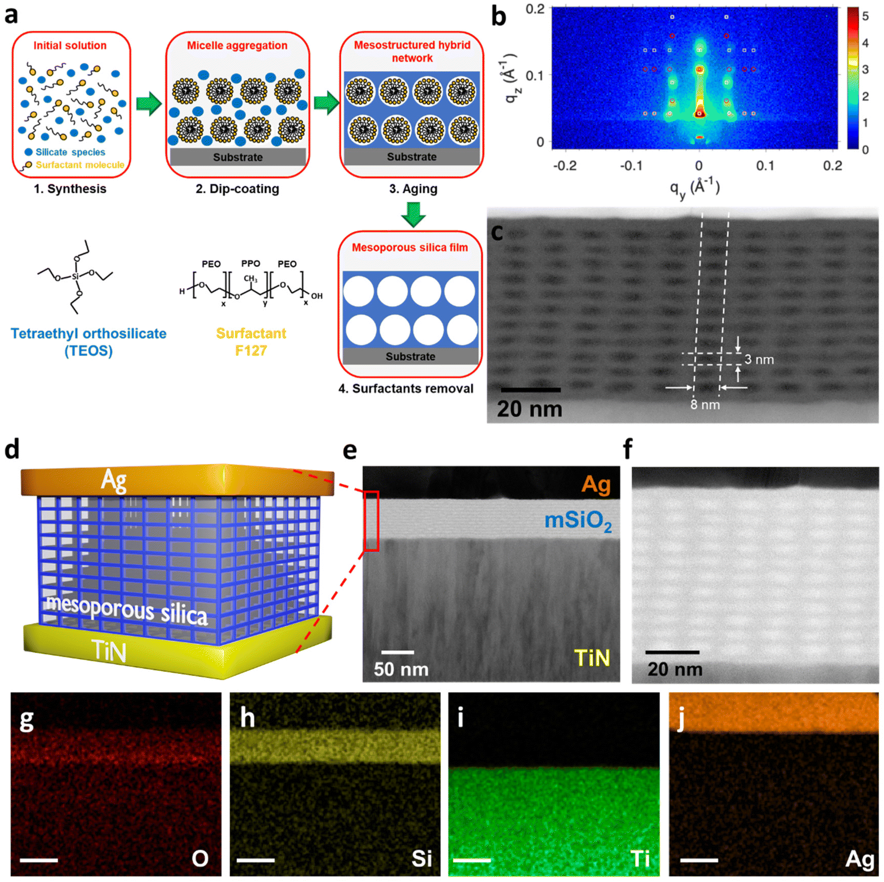 | ||
| Fig. 1 Characterization of the 3D-structured mesoporous silica thin film and memristor. (a) Fabrication process of the sol–gel mSiO2 thin films. (b) The GISAXS patterns of the mSiO2 film with simulated Bragg peaks. The red circles and white squares represent the transmitted and reflected Bragg peaks, respectively. (c) Cross-sectional TEM image of the as-deposited mesoporous silica thin film. (d) Schematic of the mSiO2 based memristor. (e) A cross-sectional TEM image of the mSiO2 memristor. (f) Higher magnification TEM image of the mSiO2 thin film in the memristor. (g–j) Cross-sectional TEM-EDX of the mSiO2 based memristor. The scale bar is 50 nm. | ||
The same mesoporous silica was deposited onto a Si/TiN substrate for memristor fabrication. The schematic of the fabricated mSiO2 memristor is shown in Fig. 1d (details of the fabrication process are in the Experimental section). The mSiO2 layer is sandwiched between an inert TiN bottom electrode and an active Ag top electrode. Fig. 1e presents the cross-sectional TEM image of a pristine mSiO2 memristor. The highly-ordered 3D-structured mesopores are clearly visible from the higher magnification TEM image in Fig. 1f. Energy-dispersive X-ray (EDX) mapping (shown in Fig. 2d–g) over the cross-sectional area also confirms the composition of each layer.
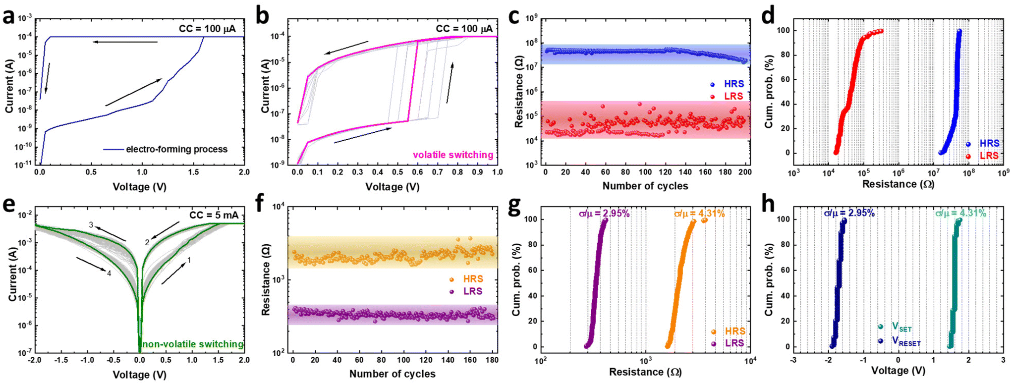 | ||
| Fig. 2 Resistive switching behavior of the 3D-structured mSiO2 based memristor. (a) I–V curve showing the formation process of the mSiO2 memristor. (b) Consecutive volatile switching I–V characteristics of the mSiO2 memristor under a CC of 100 μA. (c) Endurance characteristics and (d) cumulative probability of the HRS and LRS for volatile switching of the mSiO2 memristor. (e) Consecutive I–V characteristics showing the typical non-volatile resistive switching properties of the mSiO2 memristor under a CC of 5 mA. (f) Endurance characteristics, (g) cumulative probability of the HRS and LRS, and (h) cumulative probability of VSET and VRESET for the non-volatile switching of the mSiO2 memristor. | ||
2.2. Resistive switching of the TiN/mSiO2/Ag memristor
The electrical switching properties of the memristor devices were measured by applying DC voltage sweeps between their top and bottom electrodes. Prior to resistive switching, a formation step was required to initiate memristor switching in the devices. Fig. 2a shows that the formation occurred at approximately +1.6 V under a current compliance (CC) of 100 μA during the applied DC sweeping from 0 to 2 V. After the forming process, the device can be switched from a high resistance state (HRS) to a low resistance state (LRS) upon the application of a DC sweep from 0 to +1 V under a low CC of 100 μA as shown in Fig. 2b. The device remained in the LRS during the reversed sweep voltage and then switched back to its HRS as soon as the applied voltage reached zero or close to zero without a RESET process. This spontaneous current decay indicates a volatile switching behavior. Fig. 2c exhibits a reproducible cycling endurance in the DC sweep mode for 200 cycles. The resistance ratio between the HRS and LRS is about 3 orders of magnitude at 0.2 V. Both the HRS and LRS showed excellent uniformity without significant degradation. Fig. 2d plots the cumulative probability distributions for the HRS and LRS. Similar volatile switching behaviors were observed in further mSiO2 memristor devices when switching under low CCs. The associated I–V characteristics are presented in Fig. S3 in the ESI.†Modulating the CC level is a commonly used approach to control the resistive switching properties of memristor devices between volatile and non-volatile behaviors.35–37 Besides the volatile (temporal) memory behavior, our mSiO2 memristor also demonstrates non-volatile (non-temporal) memory behavior when the devices are operated at higher CC (1 mA and above). Fig. 2e shows the successive I–V characteristics of a DC swept between ±2 V with a current compliance (CC) of 5 mA. The graph clearly shows the typical clockwise bipolar resistive switching behavior. The direction of the current sweep is indicated by the arrows. After switching the memristor to the LRS under a CC of 5 mA, the LRS was maintained after the bias is removed. To switch the memristor back to the HRS, a RESET process was required. The DC endurance of the memristor is plotted in Fig. 2f with over 180 cycles. The resistance ratio between the HRS and LRS is about 1 order of magnitude at 0.5 V, which is sufficient for memory applications. Both the HRS and LRS showed excellent uniformity without significant degradation. To elucidate further the switching stability of the cell, cumulative probability distributions for the HRS and LRS are plotted in Fig. 2g. The figure clearly shows that the HRS and LRS are uniformly distributed with the coefficients of variation (σ/μ, σ is the standard deviation and μ is the mean value) calculated to be 15.95% and 8.57% for the HRS and LRS, respectively. Furthermore, high uniformities were also observed for both VSET and VRESET as shown in Fig. 2h, where the coefficients of variation were 4.31% and 2.95%, respectively. The high uniformities of both programming voltages are essential for large-scale ReRAM applications. Similar bipolar switching characteristics were obtained from multiple devices (Fig. S4†), showing good reproducibility of our mSiO2 based-memristor. Space-charge-limited-current (SCLC) was found to be the dominating conduction mechanism for the memristor at the HRS while ohmic conduction was observed in the LRS (Fig. S5†).
To elucidate the switching mechanism of our mSiO2 memristor, TEM and EDX characterisation studies (shown in Fig. 3a–e) were conducted on a device that has been switched several times before it was left at the HRS. In comparison with the as-fabricated device (shown in Fig. 1e), the switched device contained Ag conical dendrites that had grown from the Ag top electrode towards the TiN bottom electrode (Fig. 3a and b, more TEM images in ESI Fig. S6†). This suggests that the switching behavior of mSiO2 can be largely ascribed to the formation and rupture of Ag conductive filament(s) across the device. Similar mechanisms have also been reported in other works.38,39 It is very interesting to notice that the Ag dendrites are found within the highly-ordered mesopore structure, which acts as a pathway for the drift and diffusion of Ag ions. Based on the experimental results, the switching mechanism at different CCs is proposed and schematically presented in Fig. 3f. Upon the electroforming process, which is induced by the application of positive voltage on the active Ag top/TiN bottom electrode, the active Ag atoms are oxidized to Ag+ ionic species and migrate through the 3D-structured mSiO2 thin film following the electric field direction. After capturing electrons, these Ag+ ions are reduced and precipitate into nanoclusters at or near the TiN inert electrode (Fig. 3f-ii). These nanoclusters grow as more Ag atoms accumulate on top of them and form conductive filaments within the mSiO2 layer. When the grown conductive filament(s) connects the top and bottom electrodes, the device switches to the LRS (Fig. 3f-iii). In the case of a small CC (100 μA), the grown conductive filament is weak and the Ag atoms can spontaneously diffuse through the 3D mesopores, causing an automatic transition from the LRS to the HRS without the RESET process (Fig. 3f-iv). It has been suggested that the internal atomic rearrangement of filaments is strongly related to the interface between the filament and dielectric film during the electrochemical metallization process.40 Formation of voids in the SiO2 layer has been proved to facilitate the movement of Ag species in the dielectric layer due to reduced energy.41 The spontaneous movement of Ag atoms within our mSiO2 is therefore not surprising, considering the tremendous number of voids generated by 3D mesoporous structures. These voids contribute to the lower interfacial energy and atom strain energy,31 leading to low switching voltages (ca. 0.5 V for volatile switching and ca. ±1.5 V for non-volatile switching). On the other hand, such 3D mesopore structures also induce spontaneous dissolution of unstable and weak Ag filament(s) after the withdrawal of bias, resulting in the volatile switching behavior. Similar instability of nanowires in mesoporous silica films has been reported before.42 In the case of a large CC (5 mA), the grown conductive filament(s) across the mSiO2 thin film is large and stable (Fig. 3f-v), resulting in non-volatile switching behavior (the device retains its LRS). In this case, a sufficiently large voltage of opposite polarity is required to rupture the conductive filament(s) and therefore to switch the device to its initial HRS (Fig. 3f-vi). Given the high mobility of Ag in the mSiO2 film, it is likely for the Ag ions at the bottom mSiO2/TiN interface to drift swiftly back to the top electrode under the negative bias, resulting in residual Ag dendrites at the Ag/mSiO2 interface as suggested by the TEM image in Fig. 3a.
 | ||
| Fig. 3 (a) A cross sectional TEM image for the switched 3D-structured mSiO2 based memristor showing the conical nanoscale grown Ag filaments within the mSiO2 insulator thin film. (b–e) Cross-sectional TEM-EDX of the mSiO2 memristor. The scale bar is 50 nm. (f) The proposed switching mechanism of the mSiO2 based-memristor (i) consisting of filament formation after electroforming process (ii), under the application of a SET process at a low CC (iii) followed by spontaneous breakage of the filament (iv). In contrast, a high CC results in the formation of a more robust filament (v) that can only be broken by a full RESET process (vi). | ||
2.3. Neuromorphic switching of the TiN/mSiO2/Ag memristor
Multi-state switching characteristics are essential for memristors to realize the full potential of neuromorphic computing functions.43,44 Multiple resistance states can be obtained in mSiO2 based memristors by controlling the CC. Fig. 4a shows the I–V characteristics of the device at different CCs. While the HRS remains relatively constant, the resistance of the LRS consistently decreases upon increasing the CC from 50 to 500 μA, thereby demonstrating a reproducible and reliable multistate switching behavior (shown in Fig. 4b). When consecutive DC sweeps were applied, the device demonstrates an analogue switching behavior where the conductance can be modulated gradually (shown in Fig. 4c). Fig. 4d depicts the corresponding change in conductance with an increase in the number of DC stimulus sweeps (measured at 0.2 V). This clearly suggests the neuromorphic behavior of our mSiO2 based memristor where multi-state resistances can be precisely controlled by stimulus properties to realize synaptic plasticity. It is interesting to notice that the conductance prior to each stimulus is lower than that after previous stimuli. This implies the spontaneous dissolution of conductive filaments between two consecutive DC sweeps. Such automatic decay of current between two stimuli represents the typical characteristic of STP behavior which will be investigated further in the following section. | ||
| Fig. 4 Multi-state switching behavior of the 3D-structured mSiO2 based memristor. (a) I–V characteristics showing the multi-state switching behavior induced by varying the CC. (b) Endurance of the multi-state resistance states. (c) Consecutive volatile switching I–V characteristics with a CC of 100 μA and showing the analog switching behavior of the device. (d) Conductance versus pulses curve of the LRS of the device. The conductance was read at 0.2 V. | ||
A synapse can be considered as a two-terminal device whose synaptic weights can be dynamically modified and stored using voltage spikes as illustrated in Fig. 5a. Upon the arrival of an action voltage pulse at the pre-synaptic terminal, the weights in biological synapses are changed by the release of Ca2+ ions from the pre-neuron. This leads to dynamic modulation of the synaptic connection intensity between the pre- and post-synaptic neurons which forms the biological basis for brain information processing.6 After stimulation, the Ca2+ concentration restores back to its original level via extrusion through the plasma membrane and back to the synaptic cleft. This biological behavior characterizes a typical STP where the intensity of synaptic connection will return to its initial value in hundreds to thousands of milliseconds after the pre-synaptic activity ceases. STP is thought to be critical in performing computational functions relevant to spatiotemporal information processing in biological neural systems, and is critical for the implementation of hardware-based reservoir computing.11,13 This essential biological synaptic plasticity can be emulated by using the two-terminal mSiO2 based memristor proposed in this work. The top and bottom electrodes are regarded as the pre- and postsynaptic neurons while the drift and diffusion of the Ag+ ions mimic the release and restoration of Ca2+ ions. The memristor conductance can be regarded as the weight of the synapse while an increase or decrease in conductance corresponds to the enhancement or suppression of the synaptic connection. To demonstrate similar temporal dynamics of the mSiO2 memristor, electrical pulses were applied to the device and the postsynaptic current (PSC) was recorded using a read voltage of 0.1 V. As illustrated in Fig. 5b, a substantial increase in the PSC can be observed after the application of electrical pulses (1 V amplitude, 5 ms duration), indicating the formation of conducting Ag filaments in the mSiO2 layer (blue region). This PSC increment is enormous for the first pulse but attenuates after several pulse sequences. This suggests that the Ag ions can easily drift into the mSiO2 film within the first few pulses to form a conducting filament(s), thanks to the 3D porous structure. Simultaneously, the structure also facilitates the diffusion of the filament(s), leading to the slow saturation of the current where the drift and diffusion reach a balance. Once the electrical pulses are removed, the mSiO2 memristor experiences a sharp and spontaneous transition back to its original insulating state, implying the spontaneous dissolution of the Ag filaments into the mesoporous structure (pink region). This sharp transition represents a short relaxation time, and was found to be 600 μs based on the stretched-exponential based function (SEF) model (shown in Fig. S7†).45,46 It is worth mentioning that this relaxation time is significantly shorter than those reported from other bulk thin film-based memristors,17,19,21 thanks to the high Ag atom mobility offered by the unique 3D structure. Such shortened relaxation time is beneficial for enabling fast computing and processing. Fig. 5c further demonstrates the spike-rate-dependent plasticity (SRDP) behavior of the mSiO2 memristor when stimulated by pulse trains at different intervals. When multiple pulses are applied at short intervals (e.g. 5 ms, blue), the postsynaptic current will increase gradually, showing an accumulation effect of Ag ions in the mSiO2 film. On the other hand, if the interval between pulses increases (e.g. 20 ms, green), the current soon decays back to the original resting state as the redistribution of Ag ions is completed before the arrival of another pulse. Moreover, the synaptic weight in our artificial memristor synapse can also be modulated by the pulse amplitude and duration of the pulse. Spike-voltage dependent plasticity (SVDP) is demonstrated in Fig. 5d where continuous pulse trains with varying voltages (1 V, 2 V and 3 V) were applied on our memristor. It can be observed that the PSC increases remarkedly as the spike amplitude increases from 1 V to 3 V. This suggests that larger pulse voltages can trigger more Ag ions into the mSiO2 structure and result in higher device currents. Similarly, extending the duration of the pulse can also amplify the strength of the connection. This spike-duration-dependent plasticity (SDDP) behavior can be observed in Fig. 5e which shows a significantly increased response current when increasing the duration from 1 ms to 20 ms.
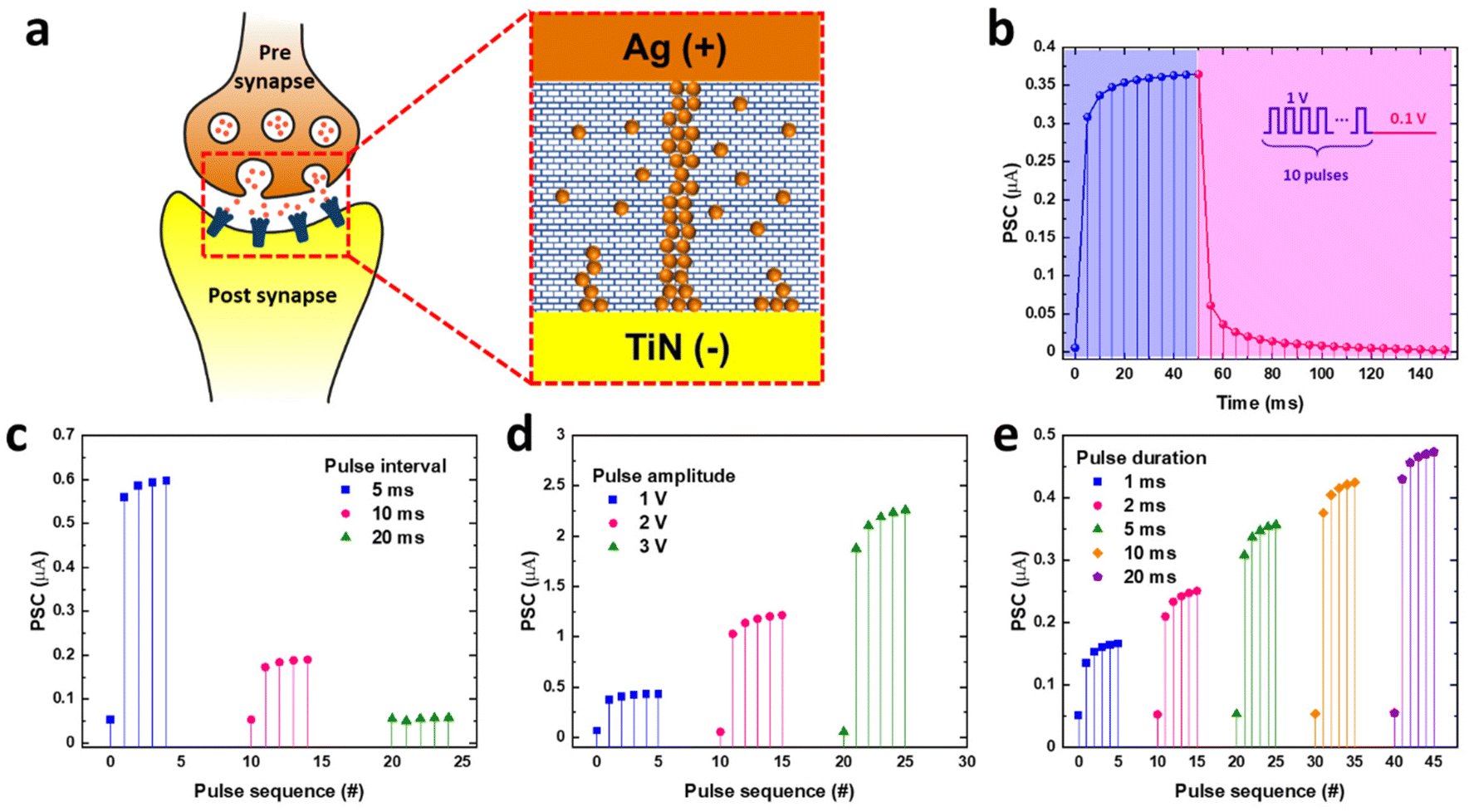 | ||
| Fig. 5 Analogy between biological-synapses and the mSiO2 memristor and short-term dynamics under pulse stimuli. (a) Schematic representation of a biological neural network and a memristor device showing the correspondence between biological and electronic synapses. (b) Gradual PSC change with a series of voltage pulses (+1 V, 5 ms duration) and the subsequent auto-decay showing STP behavior. (c) Current response of the device for pulses with different inter-spike intervals, emulating SRDP behavior. (d) Current response of the mSiO2 memristor for pulses with different voltage amplitudes, emulating SVDP behavior. (e) Current response of the mSiO2 memristor for pulses with different durations, emulating SDDP behavior. | ||
2.4. Reservoir computing using the TiN/mSiO2/Ag memristor
The unique temporal short term memory property provides our mSiO2 memristor with the capability of distinguishing input sequences with different temporal order, which is desirable for the implementation of the reservoir computing (RC) system. Fig. 6a shows the schematic of a typical RC system which consists of an input layer, a reservoir layer, and an output layer.41 The input layer interfaces the real-world information with the reservoir network. The reservoir layer, which comprises a network of randomly interconnected nodes, nonlinearly maps the temporal time-dependent input signals u(t) into a high dimensional space x(t). During the process, the connection between the input and reservoir layers is fixed while the neurons in the reservoir layer develop dynamically with temporal signals. The transient current responses based on the input signals are recorded as the reservoir states which can be read out by a simple learning algorithm through the output layer y(t). | ||
| Fig. 6 Reservoir computing system based on the mSiO2 memristor. (a) Schematic of the RC system showing the reservoir x(t) with the input u(t) layer and output y(t) layer. Win is the input weight, W is the weight of the current connection in the reservoir, and Wout is the readout weight. (b) Letter “A” as an example with a size of 5 × 5 pixels for letter recognition. (c) Schematic representation of the physical RC system including the inputs (pulse streams), the mSiO2 memristor reservoir and the readout network. (d) The recorded reservoir states for input letter “A”. (e) The response of the memristor reservoir to six different pulse streams. | ||
As a demonstration, we applied the mSiO2 memristor based RC system to perform a basic pattern recognition task to classify five different letters – “ADEPT”, short for our research project “Advanced Devices by ElectroPlaTing”. Prior to the recognition process, the pattern information needs to be firstly converted to temporal input signals. This can be achieved by treating the patterns (letters) as pixels with a size of 5 rows × 4 columns in either red (1) or white (0) colors. As an example, Fig. 6b presents the conversion of the letter “A” into a 5 × 4 pixel array. The converted array contains 5 temporal pulse sequences including signals of “0110”, “1001” and “1111” based on the spatial distribution of the red and white pixels. The pixel arrays and the associated pulse sequences for the letter “D”, “E”, “P” and “T” are listed in the ESI Fig. S8.† Each pixel-based letter was split into 5 temporal pulse sequences (3 V, 100 μs) by row to be delivered into the five selected mSiO2 memristors as shown in Fig. 6c. Here, our mSiO2 memristor acts as a physical reservoir to realize the mapping of the temporal input signal into a high dimensional space through its nonlinear dynamics and temporal memory properties offered by the drift and diffusion of Ag ions in its unique 3D connected mesoporous structure. Upon the arrival of the pulse sequences, the conductance of the mSiO2 memristor will change according to the temporal order from the pattern and the output current therefore contains the information of a spatially distributed pattern. Fig. 6d plots the recorded 5 output currents from the letter “A” where it is clear that different temporal inputs have led to different current states. The corresponding current responses from other letters are demonstrated in Fig. S8.† For the chosen 5 letters in this work, a total of six basic pulse sequences of different orders can be extracted. Fig. 6e plots the distribution of each pulse sequence from over 500 measurements based on several memristor devices. Distinct responses can be identified with sufficient margins to separate different sequences. Details of the current change for each pulse sequence are shown in Fig. S9.† These output currents are fed into the read-out function to realize pattern recognition function. The read-out function in this system is a 5 × 5 network with the 5 currents from the reservoir layer as the input and the 5 neurons representing the predicted letters as the output (shown in Fig. 6c). This network outputs the dot product of the 5 inputs and the weight associated with each output neuron, which represents the probability value of each letter. The letter with the highest probability is finally selected to be the predicted pattern. The network is trained via a supervised learning algorithm where the weights are adjusted to minimize the cross-entropy loss. More information on the network training process can be found in the Experimental section and the ESI.†
It is very important to notice that only 25 weights need to be trained in this network which is significantly smaller than that required in conventional neural networks.20 This significantly reduced network size allows the reduction of time and energy-consumption of the training process. Fig. 7a plots the training loss curve where the drastic reduction of loss can be observed within a few training epochs. This is accompanied by the increase of prediction accuracy as shown in Fig. 7b. After 20 epochs, a training accuracy of 100% was obtained, which supports the argument of a low training cost for the RC system. After the RC system was successfully trained, its performance was evaluated by recognizing letters from the test dataset which have never been seen by the system before. Fig. 7c shows the confusion matrix highlighting the experimentally obtained classification results from the RC system versus the prediction outputs (desired outputs). A recognition accuracy of 100% was achieved from the reservoir, indicating the outstanding performance of the trained mSiO2 diffusive memristor based-RC system.
 | ||
| Fig. 7 Training and performance evaluation of the mSiO2 memristor-based reservoir computing system. (a) The training and validation loss as a function of training epochs. (b) The training and validation accuracy as a function of training epochs. (c) Confusion matrix showing the prediction results from the RC system against the ground truth in the test dataset. Examples of letter patterns containing (d) one, (e) two, and (f) three random noises. Confusion matrix showing the prediction results from the RC system against the ground truth for letter patterns in the noisy test dataset containing (g) one, (h) two, and (i) three random noises. | ||
Moreover, the robustness of our RC system in pattern recognition was further tested by classifying letters with added noises. A noise test dataset was generated by randomly inverting the color for different numbers of pixels in the letter to be recognized. Fig. 7d, e, and f illustrate the examples of letters that contain 1, 2 and 3 inverted pixels (noises) in their pattern, where the noisy pixels are highlighted in red squares. Recognition accuracies of 93%, 88%, and 75% were obtained from the reservoir by including 1, 2, and 3 noisy pixels, respectively. The corresponding confusion matrices are shown in Fig. 7g–i. By introducing noisy pixels to the original images, it was found that the letters can still be recognized by the RC system even when the output signal from the reservoir is disordered.
3. Conclusions
In summary, we have successfully demonstrated a physical RC system using a 3D-structured, highly ordered mSiO2 based memristor. The memristor presents both volatile threshold switching and non-volatile bipolar switching behaviors which can be controlled by CC. The introduction of a 3D porous structure proved to facilitate the drift and diffusion of the Ag+ ion species, enabling the demonstration of the STP behavior and temporal dynamics. Such unique characteristics have been used to experimentally realize the physical RC system. Our RC system has successfully achieved in situ learning capability and a letter recognition accuracy of 100%. The demonstrated results here suggest that our diffusive memristor devices are promising candidates for artificial intelligence applications especially in temporal and sequential data processing. In addition, the potential to further tune the architecture of the mesoporous film points towards the ability to obtain better control over ion dynamics while allowing more diverse synaptic responses to the external stimuli of our mSiO2 based memristor.4. Experimental section
4.1. Chemicals
Triblock copolymer Pluronic F127 (Mw = 12![[thin space (1/6-em)]](https://www.rsc.org/images/entities/char_2009.gif) 600, PEO106–PPO70–PEO106), tetraethyl orthosilicate (TEOS), and 37% hydrochloric acid (HCl) were purchased from Sigma-Aldrich Company Ltd, and they were used without further purification. 1 M HCl was diluted from 37% HCl with deionized water. ≥99.8% Ethanol and dichloromethane (DCM) were purchased from Fisher scientific. The TiN substrates used in this study are silicon substrates coated with a 200 nm TiN layer by magnetron sputtering (Buehler Helios, rate: 0.135 nm s−1), which results in surfaces with a roughness of 1 nm. The sizes of TiN substrates are 25 × 25 mm.
600, PEO106–PPO70–PEO106), tetraethyl orthosilicate (TEOS), and 37% hydrochloric acid (HCl) were purchased from Sigma-Aldrich Company Ltd, and they were used without further purification. 1 M HCl was diluted from 37% HCl with deionized water. ≥99.8% Ethanol and dichloromethane (DCM) were purchased from Fisher scientific. The TiN substrates used in this study are silicon substrates coated with a 200 nm TiN layer by magnetron sputtering (Buehler Helios, rate: 0.135 nm s−1), which results in surfaces with a roughness of 1 nm. The sizes of TiN substrates are 25 × 25 mm.
4.2. Synthesis of mesoporous silica films
The evaporation-induced self-assembly method was used to prepare the precursor solution.34,47 The precursor solution was prepared by mixing 1.0 g of TEOS, 5.64 g of ethanol, 0.80 g of deionized water and 0.10 g of 1 M hydrochloric acid, followed by stirring at 338 K for 45 min. 0.242 g of triblock copolymer F127 was dissolved in 5.64 g of ethanol under natural conditions. The above two solutions were mixed and stirred at room temperature for 60 min. The final molar ratio of the precursor solution was TEOS:F127:HCl:H2O:EtOH = 1:0.005:0.021:9.2:51.
Dip-coating was used to coat silica films onto the TiN bottom contact. The TiN bottom contact with a thickness of 200 nm was deposited using the sputtering technique. The cleaned TiN substrates were vertically immersed in the prepared precursor solution and withdrawn at a rate of 100 mm min−1 in a 75% relative humidity chamber at 298 K. After storing in the humidity chamber (RH = 75%) for 72 h, the as-made films were aged at 120 °C for 10 h. The surfactant was removed by immersing it in the DCM solution for 4 hours and calcined at 350 °C for 5 h. Afterwards, these films were referred to as mesoporous silica films. A schematic showing the formation of mSiO2 thin films is shown in Fig. 1a.
4.3. Memristor device fabrication and characterization
After deposition, Ag top electrodes (100 nm) were deposited by e-beam evaporation through a shadow mask containing 400 μm diameter circles. High resolution X-ray diffraction patterns were obtained using a Rigaku SmartLab and performed in the wide-angle region from 10° to 100° with an incident angle of 1°. GISAXS patterns were collected using the same instrument (Rigaku SmartLab) with a Hypix-3000 Detector System, λ = 1.54 Å, and the distance between the sample and the detecting surface is around 300 mm. The incident angle was changed according to the critical angle of the samples. Destructive focused ion beam (FIB) sectioning with transmission electron microscopy (TEM) and STEM-EDX measurements have been used to characterize the composition and morphology of individual devices. The sample was imaged and analyzed by means of STEM-EDS in a doubly corrected JEOL ARM200F TEM equipped with a 1000TLE windowless Oxford Instruments spectrometer. The electrical characteristics were measured at room temperature and ambient pressure using a probe connected to a Keysight (B1500) system. For all measurements, the voltage was applied to the top electrode while the bottom electrode was grounded.4.4. Read-out network training
The readout function is trained via the supervised learning algorithm to minimize the cross-entropy loss. Before the training process, a dataset of 570 groups of current-letter pairs was experimentally measured from the memristors after being fed with different pulse streams. Herein, the current is scaled to the value with the unit of microamperes (μA); the letters, “ADEPT”, are represented by the digits 0–4 in the dataset, respectively. The obtained dataset is then split into three parts, which are the training set (80%), validation set (10%) and testing set (10%). The training set is utilized to train the neural network. The validation set works to monitor whether the neural network is overfitting or underfitting. The last part, the testing set, that has not been seen by the network, is to measure the network performance. The previously discussed neural network training is processed on a Windows PC with the CPU of Intel Core i9-9900K and the GPU of NVIDIA RTX 2070 by the open-source machine learning package PyTorch. More information on the training process can be found in the ESI.†Author contributions
The manuscript was written through contributions of all authors. All authors have given approval to the final version of the manuscript.Conflicts of interest
The authors declare no competing financial interest.Acknowledgements
This work is part of the ADEPT project funded by a Programme Grant from the EPSRC (EP/N035437/1). We also thank the EPSRC for equipment funding under EP/K00509X/1 and EP/K009877/1. All data supporting this study are openly available from the University of Southampton repository at https://doi.org/10.5258/SOTON/D2447.References
- Nat. Nanotechnol., 2020, 15, 507 Search PubMed, https://www.nature.com/articles/s41565-020-0738-x.
- A. Sebastian, M. Le Gallo, R. Khaddam-Aljameh and E. Eleftheriou, Nat. Nanotechnol., 2020, 15, 529 CrossRef CAS PubMed.
- L. F. Abbott and W. G. Regehr, Nature, 2004, 431, 796 CrossRef CAS PubMed.
- S. Kumar, X. Wang, J. P. Strachan, Y. Yang and W. D. Lu, Nat. Rev. Mater., 2022, 7, 575 CrossRef.
- G. Zhou, Z. Wang, B. Sun, F. Zhou, L. Sun, H. Zhao, X. Hu, X. Peng, J. Yan, H. Wang, W. Wang, J. Li, B. Yan, D. Kuang, Y. Wang, L. Wang and S. Duan, Adv. Electron. Mater., 2022, 2101127 CrossRef CAS.
- Y. Wu, X. Wang and W. D. Lu, Semicond. Sci. Technol., 2022, 37, 024003 CrossRef.
- D. Ielmini and H. S. P. Wong, Nat. Electron., 2018, 1, 333 CrossRef.
- S. H. Jo, T. Chang, I. Ebong, B. B. Bhadviya, P. Mazumder and W. Lu, Nano Lett., 2010, 10, 1297 CrossRef CAS PubMed.
- D. Ielmini, Microelectron. Eng., 2018, 190, 44 CrossRef CAS.
- W. Xu, J. Wang and X. Yan, Front. Nanotechnol., 2021, 3, 645995 CrossRef.
- J. Cao, X. Zhang, H. Cheng, J. Qiu, X. Liu, M. Wang and Q. Liu, Nanoscale, 2022, 14, 289 RSC.
- M. Cucchi, S. Abreu, G. Ciccone, D. Brunner and H. Kleemann, Neuromorphic Comput. Eng., 2022, 2, 032002 CrossRef.
- J. Moon, W. Ma, J. H. Shin, F. Cai, C. Du, S. H. Lee and W. D. Lu, Nat. Electron., 2019, 2, 480 CrossRef.
- G. Tanaka, T. Yamane, J. B. Héroux, R. Nakane, N. Kanazawa, S. Takeda, H. Numata, D. Nakano and A. Hirose, Neural Networks, 2019, 115, 100 CrossRef PubMed.
- K. Nakajima, Jpn. J. Appl. Phys., 2020, 59, 060501 CrossRef CAS.
- Y. Zhong, J. Tang, X. Li, B. Gao, H. Qian and H. Wu, Nat. Commun., 2021, 12, 408 CrossRef CAS PubMed.
- C. Du, F. Cai, M. A. Zidan, W. Ma, S. H. Lee and W. D. Lu, Nat. Commun., 2017, 8, 2204 CrossRef PubMed.
- G. Milano, G. Pedretti, K. Montano, S. Ricci, S. Hashemkhani, L. Boarino, D. Ielmini and C. Ricciardi, Nat. Mater., 2022, 21, 195 CrossRef CAS PubMed.
- J.-Y. Mao, Z. Zheng, Z.-Y. Xiong, P. Huang, G.-L. Ding, R. Wang, Z.-P. Wang, J.-Q. Yang, Y. Zhou, T. Zhai and S.-T. Han, Nano Energy, 2020, 71, 104616 CrossRef CAS.
- R. Midya, Z. Wang, S. Asapu, X. Zhang, M. Rao, W. Song, Y. Zhuo, N. Upadhyay, Q. Xia and J. J. Yang, Adv. Intell. Syst., 2019, 1, 1900084 CrossRef.
- H. Ryu and S. Kim, Chaos, Solitons Fractals, 2021, 150, 111223 CrossRef.
- Y. Zhou, Y. Kim, C. Jo, J. Lee, C. Wee Lee and S. Yoon, Chem. Commun., 2011, 47, 4944 RSC.
- G. E. Moehl, T. Nasir, Y. Han, Y. J. Noori, R. Huang, R. Beanland, P. N. Bartlett and A. L. Hector, Nanoscale, 2022, 14, 5404 RSC.
- Y. Wan, H. Yang and D. Zhao, Acc. Chem. Res., 2006, 39, 423 CrossRef CAS PubMed.
- Q. Gao, A. Huang, J. Zhang, Y. Ji, J. Zhang, X. Chen, X. Geng, Q. Hu, M. Wang, Z. Xiao and P. K. Chu, NPG Asia Mater., 2021, 13, 3 CrossRef CAS.
- G. Wang, Y. Yang, J. H. Lee, V. Abramova, H. Fei, G. Ruan, E. L. Thomas and J. M. Tour, Nano Lett., 2014, 14, 4694 CrossRef CAS PubMed.
- J. Kolar, J. M. Macak, K. Terabe and T. Wagner, J. Mater. Chem. C, 2014, 2, 349 RSC.
- G. Wang, J. H. Lee, Y. Yang, G. Ruan, N. D. Kim, Y. Ji and J. M. Tour, Nano Lett., 2015, 15, 6009 CrossRef CAS PubMed.
- B. Chakrabarti, H. Chan, K. Alam, A. Koneru, T. E. Gage, L. E. Ocola, R. Divan, D. Rosenmann, A. Khanna, B. Grisafe, T. Sanders, S. Datta, I. Arslan, S. K. R. S. Sankaranarayan and S. Guha, ACS Nano, 2021, 15, 4155 CrossRef CAS PubMed.
- S. H. Choi, S. O. Park, S. Seo and S. Choi, Sci. Adv., 2022, 8, 7866 CrossRef PubMed.
- B. Li, Y. Liu, C. Wan, Z. Liu, M. Wang, D. Qi, J. Yu, P. Cai, M. Xiao, Y. Zeng and X. Chen, Adv. Mater., 2018, 30, 1706395 CrossRef PubMed.
- I. Valov, E. Linn, S. Tappertzhofen, S. Schmelzer, J. Van Den Hurk, F. Lentz and R. Waser, Nat. Commun., 2013, 4, 1771 CrossRef CAS PubMed.
- S. Soulé, G. E. Moehl, R. Huang, Y. J. Noori, K. S. Kiang, C. H. Kees de Groot, R. Beanland, D. C. Smith and A. L. Hector, Nanoscale Adv., 2022, 4, 1105 RSC.
- C. J. Brinker, MRS Bull., 2004, 29, 631 CrossRef CAS.
- Y. Yang, M. Xu, S. Jia, B. Wang, L. Xu, X. Wang, H. Liu, Y. Liu, Y. Guo, L. Wang, S. Duan, K. Liu, M. Zhu, J. Pei, W. Duan, D. Liu and H. Li, Nat. Commun., 2021, 12, 6081 CrossRef CAS PubMed.
- H. Abbas, A. Ali, J. Jung, Q. Hu, M. R. Park, H. H. Lee, T.-S. Yoon and C. J. Kang, Appl. Phys. Lett., 2019, 114, 093503 CrossRef.
- C. Rebora, R. Huang, G. P. Kissling, M. Bocquet, K. De Groot, L. Favre, D. Grosso, D. Deleruyelle and M. Putero, Nanotechnology, 2019, 30, 025202 CrossRef PubMed.
- H. Abbas, Y. Abbas, G. Hassan, A. S. Sokolov, Y.-R. Jeon, B. Ku, C. J. Kang and C. Choi, Nanoscale, 2020, 12, 14120 RSC.
- A. S. Sokolov, M. Ali, R. Riaz, Y. Abbas, M. J. Ko and C. Choi, Adv. Funct. Mater., 2019, 29, 1807504 CrossRef.
- E. Budevski, G. Staikov and W. J. Lorenz, Electrochemical Phase Formation and Growth, Wiley, 1996 Search PubMed.
- Y. Yang, P. Gao, L. Li, X. Pan, S. Tappertzhofen, S. Choi, R. Waser, I. Valov and W. D. Lu, Nat. Commun., 2014, 5, 4232 CrossRef CAS PubMed.
- P. N. Bartlett, R. Beanland, J. Burt, M. M. Hasan, A. L. Hector, R. J. Kashtiban, W. Levason, A. W. Lodge, S. Marks, J. Naik, A. Rind, G. Reid, P. W. Richardson, J. Sloan and D. C. Smith, Nano Lett., 2018, 18, 941 CrossRef CAS PubMed.
- S. Petzold, E. Piros, R. Eilhardt, A. Zintler, T. Vogel, N. Kaiser, A. Radetinac, P. Komissinskiy, E. Jalaguier, E. Nolot, C. Charpin-Nicolle, C. Wenger, L. Molina-Luna, E. Miranda and L. Alff, Adv. Electron. Mater., 2020, 6, 2000439 CrossRef CAS.
- Y. Zhang, Z. Wu, S. Liu, Z. Guo, Q. Chen, P. Gao, P. Wang and G. Liu, Front. Neurosci., 2021, 15, 717222 CrossRef PubMed.
- T. Chang, S. H. Jo and W. Lu, ACS Nano, 2011, 5, 7669 CrossRef CAS PubMed.
- Z. Q. Wang, H. Y. Xu, X. H. Li, H. Yu, Y. C. Liu and X. J. Zhu, Adv. Funct. Mater., 2012, 22, 2759 CrossRef CAS.
- C. J. Brinker, Y. Lu, A. Sellinger and H. Fan, Adv. Mater., 2004, 29, 631 CAS.
Footnote |
| † Electronic supplementary information (ESI) available. See DOI: https://doi.org/10.1039/d2nr05012a |
| This journal is © The Royal Society of Chemistry 2022 |