
 Open Access Article
 This Open Access Article is licensed under a
 Creative Commons Attribution 3.0 Unported Licence
Low threading dislocation density and antiphase boundary free GaAs epitaxially grown on on-axis Si (001) substrates†
Junjie
Yang‡
 a,
Keshuang
Li‡
a,
Hui
Jia
a,
Huiwen
Deng
a,
Xuezhe
Yu
a,
Pamela
Jurczak
a,
Jae-Seong
Park
a,
Shujie
Pan
a,
Wei
Li
b,
Siming
Chen
a,
Alwyn
Seeds
a,
Mingchu
Tang
*a and
Huiyun
Liu
a
a,
Keshuang
Li‡
a,
Hui
Jia
a,
Huiwen
Deng
a,
Xuezhe
Yu
a,
Pamela
Jurczak
a,
Jae-Seong
Park
a,
Shujie
Pan
a,
Wei
Li
b,
Siming
Chen
a,
Alwyn
Seeds
a,
Mingchu
Tang
*a and
Huiyun
Liu
a
aDepartment of Electronic and Electrical Engineering, University College London, Torrington Place, London, WC1E 7JE, UK. E-mail: Mingchu.tang.11@ucl.ac.uk
bInstitute of the Microstructure and Properties of Advanced Materials, Beijing University of Technology, Beijing, 100124, China
First published on 7th November 2022
Abstract
Epitaxial growth of III–V materials on a CMOS-compatible Si (001) substrate enables the feasibility of mass production of low-cost and high-yield Si-based III–V optoelectronic devices. However, the material dissimilarities between III–V and group-IV materials induce several types of defects, especially threading dislocations (TDs) and antiphase boundaries (APBs). The presence of these defects is detrimental to the optoelectronic device performance and thus needs to be eliminated. In this paper, the mechanism of APB annihilation during the growth of GaAs on on-axis Si (001) is clarified, along with a detailed investigation of the interaction between TDs and the periodic {110} APBs. A significant reduction in the TD density ascribed to the presence of periodic APBs is discussed. This new observation opens the possibility of reducing both APBs and TDs simultaneously by utilising optimised GaAs growth methods in the future. Hence, a thin APB-free GaAs/Si (001) platform with a low TD density (TDD) was obtained. Based on this platform, a high-performance high-yield III–V optoelectronic device grown on CMOS-compatible Si (001) substrates with an overall thickness below the cracking threshold is feasible, enabling the mass production of Si-based photonic integrated circuits (PICs).
 Mingchu Tang | Dr Mingchu Tang graduated with a BEng degree from the University of Sussex in 2011 and an MSc degree in Nanotechnology from the University College London in 2012. In Oct 2016, he obtained his PhD degree in semiconductor photonics, and soon after started his postdoc job in the same research group. He is now a lecturer in the Department of Electronic and Electrical Engineering at the University College London. His interests include the heteroepitaxy growth of III–V compound semiconductor materials on III–V native and Group-IV substrates for high performance photonic devices. |
1. Introduction
Monolithic integration of III–V lasers on Si substrates has been regarded as one of the most promising candidates to realise on-chip light sources for Si-based PICs.1–3 Nevertheless, the direct epitaxy of III–V materials on Si substrates is challenging due to the large material dissimilarities between the III–V and group-IV materials. The incompatible lattice constant, thermal expansion coefficient and different polarities lead to the formation of dislocations, micro-cracks and antiphase boundaries (APBs), respectively.4,5 All these defects act as non-radiative recombination centres and significantly impede the sufficient operation of laser devices. Strategies including defect filter layers and longer cooling periods are commonly utilised to solve the threading dislocations and micro-cracks. On the other hand, APBs or the so-called inversion boundaries are planar defects arising from the deposition of polar III–V materials on non-polar Si substrates. The presence of APBs is detrimental to the performance of devices. Specifically, APBs that consist of homopolar bonds, e.g., As–As or Ga–Ga bonds, are electrically charged planar defects, which act as non-radiative recombination centres and electrical leakage paths.6–9 APBs nucleate at the edge of single-atomic-height (S) Si steps while they will be prevented by bi-atomic height (D) Si steps. Therefore, Si substrates with offcut angles of 4 or 6° are commonly implemented to form dominant D Si steps and inhibit the formation of APBs.10–12 However, offcut Si substrates are incompatible with the well-established CMOS processing technology, which needs nominal Si (001) substrates with a miscut angle of less than 0.5°.13–15Pioneering works on forming APB-free III–V materials monolithically grown on Si (001) have shown impressive results. By adopting V-grooved Si (111) surfaces through an aspect ratio trapping (ART) process, Li et al. successfully produced APB-free GaAs grown on a Si (001) substrate.16 With the help of high-temperature annealing of Si substrates under a hydrogen atmosphere, Kunert et al. and Alcotte et al. reported the preparation of APB-free GaP-on-Si and GaAs-on-Si using the metalorganic chemical vapour deposition technique.7,17 However, these approaches demand hydrogen sources and minimum selected offcut angles (0.12° for GaP-on-Si and 0.15° for GaAs-on-Si). These selected angles require Si substrates to be measured before the growth, which is unfavourable for molecular beam epitaxy (MBE) growth and massive production. On the other hand, MBE has a unique advantage in producing high-quality III–V quantum dots (QDs), which have been regarded as one of the most promising candidates for the gain medium to achieve practical Si-based on-chip light sources.3 Recently, there have been a few reports on all-MBE grown APB-free III–V materials on Si (001) substrates. Kwoen et al. reported that a high-temperature AlGaAs nucleation layer (NL) was used to form an APB-free GaAs layer,18 although the mechanism behind this scheme remains unclear. Most recently, Li et al. illustrated that the use of periodic parallel Si S steps contributed to the annihilation of APBs in GaAs-on-Si.19 This observation was later confirmed by Calvo et al. in a GaSb-on-Si system.20 Based on these methods, high-performance III–V lasers monolithically grown on Si (001) have been successfully demonstrated.13–15,21,22
In this work, we investigated the impact of a low-temperature grown AlGaAs NL on APB annihilation and discussed the annihilation of APBs in the following GaAs layer where non-annealing and growth-during-ramp methods are implemented. In the meantime, the interaction between TDs and the periodic {110} APBs has been investigated in a GaAs/Si (001) system with clear evidence. A significant reduction in the TDD ascribed to the presence of periodic APBs was observed, which would benefit from a low-thickness III–V buffer on Si for the preparation of low-cost and high-yield Si-based PICs.
2. Results and discussion
2.1 Material growth
Material growth was carried out using a twin-MBE system, which consists of a group-IV and a III–V reactor. On-axis Si (100) substrates with a 0.15 ± 0.1° miscut toward the 〈110〉 orientation were loaded in the group-IV MBE reactor first (note that the offcut angles of Si substrates were not selected). Prior to the growth, the Si (001) substrate was deoxidised at 1200 °C for 30 min. A 100 nm Si buffer layer was deposited at 850 °C on the deoxidised substrate using a Si e-beam source, followed by five iterations of 20 nm Si grown at 850 °C and annealed at 1200 °C to form a surface-reconstructed Si buffer layer with parallel Si S steps. The GaAs grown on the Si buffer layer with various iterations of Si thin layers is shown in Fig. S1 in the ESI.† According to Chadi's nomenclature, these S steps can be classified into two types, Sa and Sb, depending on whether the step edge is perpendicular or parallel to the dimer rows on the upper terrace, respectively.23 The detail of the Si steps and their impact on APB annihilation can be found elsewhere in Li et al.19 The wafer was then transferred to the III–V MBE reactor through an ultra-high-vacuum transfer chamber, which avoids contamination and ensures a clean Si epi-surface. The crystallographic information of grown samples was analysed by high-resolution transmission electron microscopy (TEM), atomic force microscopy (AFM) and electron channelling contrast imaging (ECCI) measurements.Two samples were grown to examine the impact of temperature ramping on APB propagation and annihilation. The structure of sample A is shown in Fig. 1(a). Since our III–V MBE system is equipped with two Ga sources, it is capable of adjusting the growth rates of Ga for specific layers, e.g., 0.1, 0.6 and 0.7 monolayers per second (ML s−1). A 40 nm Al0.4Ga0.6As NL (later represented by AlGaAs NL) was deposited on the Si buffer layer at 330 °C at a low growth rate of 0.1 ML s−1. A ramping step at a ramping rate of 10 °C min−1 was applied afterwards. This ramping rate was also applied in the following temperature-ramping steps. Once the temperature reached 350 °C, a 210 nm low-temperature (LT) GaAs layer was grown, followed by another ramping process to 420 °C to initiate the growth of the 250 nm mid-temperature (MT) GaAs layer. After the third ramping process, the growth temperature reached the desired value of 580 °C for the growth of another 500 nm high-temperature (HT) GaAs layer. During the growth of the HT GaAs layer, the growth rate of GaAs increased to 0.7 ML s−1 to ensure the high crystal quality. Finally, the whole thickness of the GaAs buffer layer reached 1 μm. In contrast, for sample B, the temperature-ramping steps applied to sample A were replaced by temperature-ramped growth steps. At the same time as the temperature ramping, GaAs was deposited at a growth rate of 0.6 ML s−1 and the total thickness of sample B was kept at 1 μm, as shown in Fig. 1(b). Furthermore, a temperature versus growth time plot of both the samples is shown in Fig. 1(c).
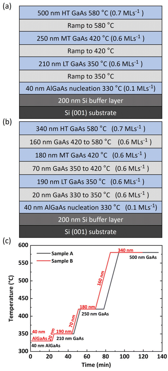 | ||
| Fig. 1 Schematic structures showing 3-step GaAs grown on Si (001) substrates for (a) sample A and (b) sample B. (c) Temperature versus growth time for samples A and B. | ||
2.2 Growth-during-ramp method
In contrast to the study proposed previously, AlGaAs with a low growth temperature of 330 °C is proposed to achieve an APB-free GaAs buffer layer.18 During the LT growth, the APBs resemble the distribution of underlying Si steps mainly propagating through the energy-favoured {110} planes, in which the APB consists of an equal number of Ga–Ga and As–As wrong bonds. However, these {110} APBs are unstable – a slight increase in the temperature would enhance the migration of atoms of wrong bonds and form an APB-modified thermodynamic equilibrium (APB-MTE), as previously reported by Guo et al.24 In this case, a (110) APB tends to enlarge while two antiphase domains (APDs) with single-phase grains are formed, leaving a deep gap in between. As a result, a high APB density and surface roughness are observed in sample A, as shown in Fig. 2(a), showing degraded crystal quality. In stark contrast, as shown in Fig. 2(b), the GaAs layer with an LT AlGaAs NL formed using a growth-during-ramp method shows a typical APB-free surface while special patterns are formed as a result of the underlying APB annihilation. The mechanism of forming mono-phase grains is shown in Fig. 3(a). During the temperature-ramping process without GaAs growth, the migration of atoms leads to an APB-MTE in which APDs with mono-phase grains are formed.24 On the other hand, as for the temperature-ramped growth process, the deposition of GaAs during the temperature-ramping step elongates the {110} APBs. Hence, a higher energy is required to achieve the APB-MTE. A combination of a high GaAs growth rate along with a moderate temperature-ramping rate (in this case, 0.6 ML s−1 and 10 °C min−1, respectively) is crucial to maintain the balance and prevent the formation of an APB-MTE. This temperature-ramped growth process also helps to reconfigure the APBs into higher index planes when sufficient high temperature is applied, leading to the annihilation of APBs, as shown in Fig. 3(b).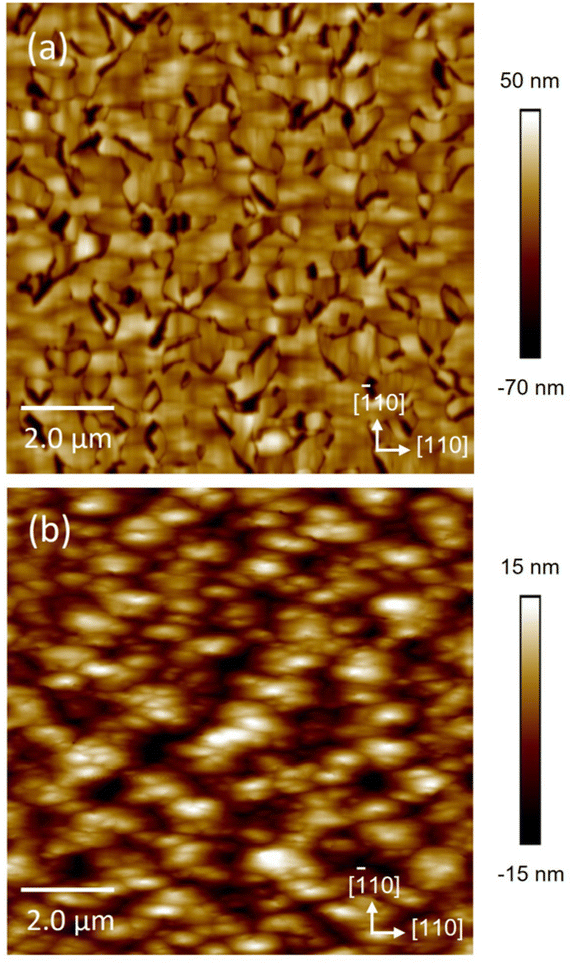 | ||
| Fig. 2 10 × 10 μm2 AFM measurements of a 1 μm GaAs surface grown on Si (001) substrates (a) without and (b) with the growth-during-ramp method. | ||
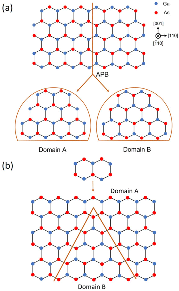 | ||
| Fig. 3 Schematic diagrams of (a) the APB-modified thermodynamic equilibrium during the temperature ramping process where single-phase grain domains are formed and (b) the deposition of GaAs during the temperature-ramped growth process prevents the enlargement of APBs and facilitates the annihilation of APBs during the temperature increase. | ||
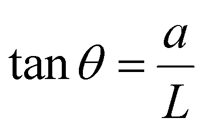
The cross-sectional TEM images of the LT AlGaAs NL, showing its impact on the APB propagation, are shown in Fig. 4. As previously reported,19 the nucleation of APBs resembles the distribution of the underlying Si steps, which are parallel S steps. Therefore, a periodic array of APBs is observed in Fig. 4(a). The distance between two neighbouring APBs equals the terrace width of adjacent Si S steps, which is related to the miscut angle θ of the used Si (001) substrate. This relationship is defined as
 | ||
| Fig. 4 Bright-field TEM images showing (a) equally distributed APBs on Si (001) with an AlGaAs NL, which is the same for APBs nucleated on a GaAs NL. (b) In some areas, the AlGaAs NL was found to promote the annihilation of APBs. | ||
2.3 APB annihilation mechanism
APBs consist of homopolar bonds, e.g., the As–As bond or Ga–Ga bond, and propagate inside the epilayer during the growth of GaAs on exactly oriented Si (001). The APBs mainly propagate through the {110} or higher index planes, such as {112} and {111} planes. The formation energies of APBs in different index planes have been studied by Rubel et al.25 The {110} APBs have the lowest formation energy of 28 meV Å−2, compared with the {112} and {111} APBs, which have the formation energies of 39 and 43 meV Å−2, respectively. During the overgrowth of the GaAs layer, the space between neighbouring APBs becomes narrower with an increase in the vertical distance from the GaAs/Si interface. Apart from the thermally induced reconfiguration of the APB propagation planes, an extra factor contributing to the incline of APBs depends on the preferred growth direction of GaAs.Ohta et al. and Horikoshi et al. investigated the orientation-dependent diffusion length of Ga adatoms on a GaAs (001) substrate.26,27 The diffusivity of Ga along the As dimer direction is four times larger than that of Ga perpendicular to the As dimer direction. Since the growth of GaAs on the Si buffer layer starts with the As pre-layer, by providing excess As due to the low sticking coefficient of As on Si, a similar observation is anticipated. Specifically, Ga adatoms, parallel to the As dimer orientation (the same as the Si dimer orientation), are expected to exhibit a higher diffusion length. Therefore, GaAs grown on the upper terrace of Sa (main-phase) and Sb prefers to grow along the [110] and [1−10] directions, respectively, as shown in Fig. 5(a). Along the [110] direction, the main phase GaAs has a slightly higher growth rate than the antiphase GaAs, forcing the neighbouring high index plane APBs to move towards each other as the temperature increases during the GaAs overgrowth. Consequently, the width of the APB becomes smaller during the temperature-ramping process, and suppression of the APB within the GaAs buffer layer is facilitated. A similar result was also reported for GaSb-based systems by Calvo et al.20 This observation explains the high rate of APB self-annihilation during the growth of the three-step GaAs on the surface-reconstructed Si buffer layer, and a 1 μm-thick APB-free GaAs/Si (001) platform was obtained consequently.
 | ||
| Fig. 5 (a) Growth preference of III–V materials along with different types of Si S steps. (b) Schematic diagram showing the annihilation of APBs where the anti-phase is fully covered by the main phase. | ||
2.4 Interaction between APBs and TDs
Direct epitaxy of III–V materials on Si substrates faces significant challenges due to the large material dissimilarities between III–V and group-IV materials. The primary issue of the direct epitaxy of III–V materials on a Si substrate is the formation of TDs, which are one-dimensional defects.28,29 It has been demonstrated that the use of on-axis Si substrates induces a higher level of TDs than offcut Si substrates during GaAs epitaxy as a result of less uniform Si step distribution in on-axis Si (001) substrates.28 A high TDD of 108 cm−2 has been reported for 2.3 μm GaAs grown on Si (001) substrates, and such a high TDD is three-fold higher than that of GaAs grown on offcut Si substrates under similar growth conditions.30 The high-density TDs propagate freely towards the active region, resulting in a degradation of the device performance. The presence of a high TD density in the active region generates extra heat during device operation. On the other hand, APBs are planar defects that arise from the growth of polar III–V materials on non-polar Si (001) substrates, which nucleate at the Si S step edge and penetrate through the III–V epilayer. The termination of APBs is achieved when two APBs intersect and form a closed loop, leaving the upper III–V material antiphase disorder free.5 Both defects, which originate from the III–V/Si interface, are detrimental to the material quality and degrade the electronic and optical properties of the device. Therefore, a proper understanding of the interaction of TDs and APBs is necessary using cross-sectional TEM measurements, which is presented in Fig. 6(a) and (b).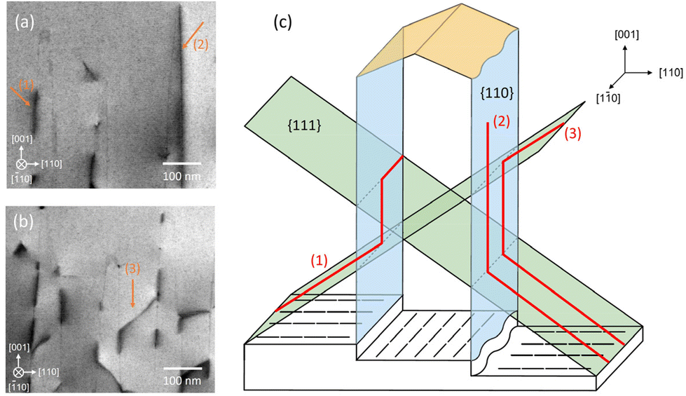 | ||
| Fig. 6 Cross-sectional bright-field TEM images showing the interaction between TDs and the APBs. (a) TD propagates along with the APBs. (b) TDs are trapped between neighbouring APBs forming an APB–TD network. (c) A schematic diagram showing the interaction between the APBs and TDs. TDs that are darker than the APB lines are marked by orange arrows in (a and b) and red lines in (c). The numbers (1), (2) and (3) represent three cases of interaction between TDs and the APBs. | ||
As previously mentioned, the nucleated APBs resemble the distribution of underlying parallel Si S steps and have ordered distribution. The termination of APBs is promoted by kinking the APBs into higher index planes during the temperature increase in GaAs overlayer growth. As a result, the periodic self-annihilated APBs in the {110} planes are presented in Fig. 6(a) and (b). In the GaAs/Si system, glissile dislocations commonly glide on the {111} planes, which have the lowest Peierls barrier and are considered as easy slip planes for TDs in GaAs.28,31 As shown in Fig. 6(a), the presence of APBs bends the TDs from their {111} glide planes to the (110) APB propagation plane and allows TDs to propagate along the {110} APBs. A possible explanation is that APBs consist of homopolar bonds which make the lattice in GaAs no longer conserved. As a result, TDs are able to climb along the {110} planes during the GaAs overgrowth. This observation is similar to that reported in a GaSb/Si system.32,33 APBs, which act as traps, provide space for TDs to propagate, leading to a higher possibility of TD self-annihilation if two TDs with opposite Burgers vector signs meet with each other. This APB–TD interaction mechanism is illustrated as the red line (2) in Fig. 6(c). Clear evidence of this case is given by the ECCI measurements shown in Fig. 7, where the TDs (represented by dots) are well organised along the parallel APBs. In other cases, before the termination of TDs occurs, some TDs that propagate along the {110} planes will bend again into new {111} glide planes and move towards the intersecting line along the [110] direction. Consequently, some TDs can only be observed as segments, as shown in Fig. 6(a). This APB–TD interaction scenario is represented by the red line (1) in Fig. 6(c).
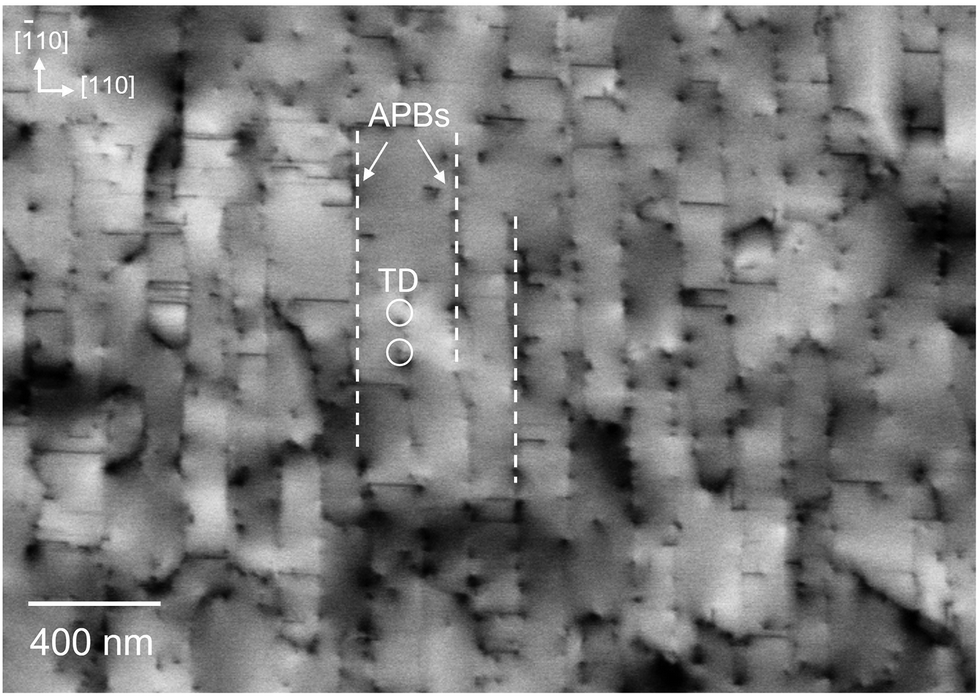 | ||
| Fig. 7 Top-view ECCI image showing the distribution of TDs along the periodic APBs for MT GaAs (500 nm). TDs and APBs are labelled as white circles and straight lines, respectively. | ||
As shown in Fig. 6(b), several TDs propagate along the periodic APBs and form TD networks. This phenomenon is observed for the first time. A possible explanation is given in the following. The presence of {110} APBs bends the TDs from their {111} glide planes to along the {110} planes. Once the TDs reach another {111} plane, they start to propagate along the easy slip {111} planes again and will be captured by another APB to repeat the process. This process will continue until TDs are self-annihilated or move beyond the presence of periodic APBs. This kind of APB–TD interaction is illustrated by the red line (3) in Fig. 6(c). Consequently, the TDD level is expected to be significantly reduced in the presence of periodic APBs.
A large-scale cross-sectional TEM image showing the APB–TD interaction within 1 μm GaAs is presented in Fig. 8(a). Commonly, a high TDD (1010 cm−2) arises from the GaAs/Si (001) interface and propagates towards the active region. The presence of periodic APBs traps the TDs and increases the possibility of TDs with opposite Burgers vector signs to meet and self-annihilate with each other. As a result, a sharp reduction in the TD density is expected. A TDD of 8 × 108 cm−2 was obtained for 1 μm GaAs grown on on-axis Si (001), where all APBs are terminated underneath, as shown in the ECCI measurement of Fig. 8(b). To make a comparison of the TDD without the impact of APBs, a 1 μm GaAs layer has been grown on a Si offcut substrate, where the growth structure is illustrated in the reference.1 The TDD value of GaAs grown on an on-axis Si (001) substrate was approximately half that of 1 μm GaAs grown on an offcut Si substrate with a similar structure, as presented in Fig. 8(c). Nevertheless, the TDD of 8 × 108 cm−2 remains high for the GaAs buffer layer, and InGaAs/GaAs defect filter layers will be introduced later to minimise the TDD to around ∼5 × 106 cm−2 and ensure a high-performance operation of optoelectronic devices.34
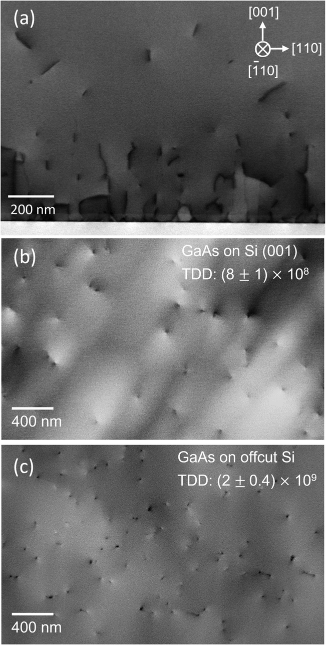 | ||
| Fig. 8 (a) Cross-sectional bright-field TEM image of GaAs grown on an on-axis Si (001) substrate. ECCI image showing the TD density of GaAs grown on (b) a Si (001) substrate and (c) an offcut Si substrate. | ||
Previous research has reported that the presence of APBs forms impassable obstacles to glissile TDs, leading to a higher TDD in GaAs monolithically grown on Si (001).35 This conclusion has also been reported in other studies.30,31 Based on our observation, it is true that TDs are unable to penetrate APBs; instead, TDs will be bent by APBs and propagate along the APBs in the subsequent growth. Furthermore, our results indicate that periodic APBs promote the propagation and termination of TDs within the APBs before propagating towards the active region, which is in contrast to the previous conclusion.35 This new observation opens up the possibility of reducing both the APBs and TDs simultaneously, specifically a thin APB-free GaAs/Si (001) with a low TDD, by optimising GaAs growth methods. Based on this platform, a high-performance micro-crack-free InAs/GaAs QD laser grown on Si (001) with a reduced overall thickness below the cracking threshold (∼5 μm) is feasible, which offers a path towards the realisation of PICs on a single substrate with a high yield and a low cost.
3. Conclusions
In this paper, we have demonstrated that Al atoms with strong intra-bonding bend the propagation of APBs and promote their self-annihilation within the AlGaAs NL, leaving a lower density of APBs to propagate towards the GaAs buffer layer. Furthermore, our three-step GaAs growth strategy along with non-annealing and growth-during-ramp GaAs subsequent growth methods reconfigures the propagation planes of {110} APBs and promotes their self-annihilation because of different growth rates in the main-phase and antiphase GaAs.Finally, the interaction between the {110} APBs and TDs is discussed. The APBs bend the TDs from the {111} slip planes to the {110} APB propagation planes and enhance the TD self-annihilation. In some cases, the TDs that propagate along the {110} planes will bend again into new {111} glide planes. These TDs will either move towards the intersecting line or propagate further, the latter of which is likely to be captured by other APBs forming TD networks until TDs are terminated or move beyond a place where the APBs no longer exist. Therefore, the periodic array of APBs enhances the TD self-annihilation. A dramatic reduction in the TDD from ∼1010 to 8 × 108 cm−2 was observed in the GaAs on Si (001) with the presence of ordered APBs. This new observation opens up the possibility of reducing both the APBs and TDs simultaneously by utilising optimised GaAs growth methods. Hence, a thin APB-free GaAs/Si (001) platform with a low TDD was obtained. Based on this platform, the formation of a high-performance high-yield InAs/GaAs QD laser grown on a CMOS-compatible Si (001) substrate with an overall thickness below 5 μm is feasible, enabling the realisation of Si-based PICs with a high yield and a low cost.
Author contributions
M. T. and H. L. proposed and guided the overall project. J. Y., K. L., M. T., P. J., X. Y. and H. L. performed the material growth. H. J. performed the ECCI characterisation. J. Y., S. P. and H. D. carried out the AFM characterisation. W. L. performed the TEM characterisation. J. Y., M. T., J. P., A. S., S. C. and H. L. composed and revised the manuscript.Conflicts of interest
There are no conflicts to declare.Acknowledgements
The UK Engineering and Physical Sciences Research Council (EPSRC) under grants EP/V029606/1, EP/P006973/1, EP/T028475/1, and EP/X015300/1, and the Royal Academy of Engineering (RF201617/16/28) are acknowledged. JY acknowledges the CSC scholarship.References
- S. Chen, W. Li, J. Wu, Q. Jiang, M. Tang, S. Shutts, S. N. Elliott, A. Sobiesierski, A. J. Seeds, I. Ross, P. M. Smowton and H. Liu, Nat. Photonics, 2016, 10(5), 307–311 CrossRef.
- Z. Zhou, B. Yin and J. Michel, Light: Sci. Appl., 2015, 4(11), e358–e358 CrossRef CAS.
- M. Tang, J.-S. Park, Z. Wang, S. Chen, P. Jurczak, A. Seeds and H. Liu, Prog. Quantum Electron., 2019, 66, 1–18 CrossRef.
- E. Tournié, L. Cerutti, J.-B. Rodriguez, H. Liu, J. Wu and S. Chen, MRS Bull., 2016, 41(03), 218–223 CrossRef.
- B. Kunert, Y. Mols, M. Baryshniskova, N. Waldron, A. Schulze and R. Langer, Semicond. Sci. Technol., 2018, 33(9), 093002 CrossRef.
- H. Kroemer, J. Cryst. Growth, 1987, 81(1–4), 193–204 CrossRef.
- R. Alcotte, M. Martin, J. Moeyaert, R. Cipro, S. David, F. Bassani, F. Ducroquet, Y. Bogumilowicz, E. Sanchez, Z. Ye, X. Y. Bao, J. B. Pin and T. Baron, APL Mater., 2016, 4(4), 046101 CrossRef.
- M. Martin, D. Caliste, R. Cipro, R. Alcotte, J. Moeyaert, S. David, F. Bassani, T. Cerba, Y. Bogumilowicz, E. Sanchez, Z. Ye, X. Y. Bao, J. B. Pin, T. Baron and P. Pochet, Appl. Phys. Lett., 2016, 109(25), 253103 CrossRef.
- A. Beyer and K. Volz, Adv. Mater. Interfaces, 2019, 6(12), 1801951 CrossRef.
- J. Yang, Z. Liu, P. Jurczak, M. Tang, K. Li, S. Pan, A. Sanchez, R. Beanland, J.-C. Zhang and H. Wang, J. Phys. D: Appl. Phys., 2020, 54(3), 035103 CrossRef.
- J. Yang, P. Jurczak, F. Cui, K. Li, M. Tang, L. Billiald, R. Beanland, A. M. Sanchez and H. Liu, J. Cryst. Growth, 2019, 514, 109–113 CrossRef CAS.
- A. D. Lee, Q. Jiang, M. Tang, Y. Zhang, A. J. Seeds and H. Liu, IEEE J. Sel. Top. Quantum Electron., 2013, 19(4), 1901107–1901107 Search PubMed.
- A. Y. Liu, J. Peters, X. Huang, D. Jung, J. Norman, M. L. Lee, A. C. Gossard and J. E. Bowers, Opt. Lett., 2017, 42(2), 338–341 CrossRef CAS PubMed.
- D. Jung, J. Norman, M. J. Kennedy, C. Shang, B. Shin, Y. Wan, A. C. Gossard and J. E. Bowers, Appl. Phys. Lett., 2017, 111(12), 122107 CrossRef.
- S. Chen, M. Liao, M. Tang, J. Wu, M. Martin, T. Baron, A. Seeds and H. Liu, Opt. Express, 2017, 25(5), 4632–4639 CrossRef CAS.
- Q. Li, K. W. Ng and K. M. Lau, Appl. Phys. Lett., 2015, 106(7), 072105 CrossRef.
- B. Kunert, I. Németh, S. Reinhard, K. Volz and W. Stolz, Thin Solid Films, 2008, 517(1), 140–143 CrossRef CAS.
- J. Kwoen, J. Lee, K. Watanabe and Y. Arakawa, Jpn. J. Appl. Phys., 2019, 58(SB), SBBE07 CrossRef.
- K. Li, J. Yang, Y. Lu, M. Tang, P. Jurczak, Z. Liu, X. Yu, J.-S. Park, H. Deng, H. Jia, M. Dang, A. M. Sanchez, R. Beanland, W. Li, X. Han, J.-C. Zhang, H. Wang, F. Liu, S. Chen, A. Seeds, P. Smowton and H. Liu, Adv. Opt. Mater., 2020, 8(22), 2000970 CrossRef.
- M. Rio Calvo, J. B. Rodriguez, C. Cornet, L. Cerutti, M. Ramonda, A. Trampert, G. Patriarche and E. Tournié, Adv. Electron. Mater., 2022, 8(1), 2100777 CrossRef.
- K. Li, Z. Liu, M. Tang, M. Liao, D. Kim, H. Deng, A. M. Sanchez, R. Beanland, M. Martin, T. Baron, S. Chen, J. Wu, A. Seeds and H. Liu, J. Cryst. Growth, 2019, 511, 56–60 CrossRef.
- M. R. Calvo, L. M. Bartolomé, M. Bahriz, G. Boissier, L. Cerutti, J.-B. Rodriguez and E. Tournié, Optica, 2020, 7(4), 263–266 CrossRef CAS.
- O. Alerhand, A. N. Berker, J. Joannopoulos, D. Vanderbilt, R. Hamers and J. Demuth, Phys. Rev. Lett., 1990, 64(20), 2406 CrossRef CAS.
- W. Guo, A. Bondi, C. Cornet, A. Létoublon, O. Durand, T. Rohel, S. Boyer-Richard, N. Bertru, S. Loualiche and J. Even, Appl. Surf. Sci., 2012, 258(7), 2808–2815 CrossRef CAS.
- O. Rubel and S. D. Baranovskii, Int. J. Mol. Sci., 2009, 10(12), 5104–5114 CrossRef CAS.
- K. Ohta, T. Kojima and T. Nakagawa, J. Cryst. Growth, 1989, 95(1–4), 71–74 CrossRef CAS.
- Y. Horikoshi, M. Kawashima and H. Yamaguchi, Jpn. J. Appl. Phys., 1988, 27(2), 169–179 CrossRef CAS.
- R. Beanland, D. Dunstan and P. Goodhew, Adv. Phys., 1996, 45(2), 87–146 CrossRef CAS.
- J.-S. Park, M. Tang, S. Chen and H. Liu, Crystals, 2020, 10(12), 1163 CrossRef.
- R. Fischer, D. Neuman, H. Zabel, H. Morkoc, C. Choi and N. Otsuka, Appl. Phys. Lett., 1986, 48(18), 1223–1225 CrossRef.
- S. F. Fang, K. Adomi, S. Iyer, H. Morkoç, H. Zabel, C. Choi and N. Otsuka, J. Appl. Phys., 1990, 68(7), R31–R58 CrossRef.
- M. Niehle, A. Trampert, J.-B. Rodriguez, L. Cerutti and E. Tournié, Scr. Mater., 2017, 132, 5–8 CrossRef.
- M. Niehle, J.-B. Rodriguez, L. Cerutti, E. Tournié and A. Trampert, Phys. Status Solidi, 2019, 13(10), 1900290 Search PubMed.
- M. Tang, S. Chen, J. Wu, Q. Jiang, K. Kennedy, P. Jurczak, M. Liao, R. Beanland, A. Seeds and H. Liu, IEEE J. Sel. Top. Quantum Electron., 2016, 22(6), 50–56 Search PubMed.
- E. P. Kvam, J. Electron. Mater., 1994, 23(10), 1021–1026 CrossRef.
Footnotes |
| † Electronic supplementary information (ESI) available. See DOI: https://doi.org/10.1039/d2nr04866c |
| ‡ These authors contributed equally to this work. |
| This journal is © The Royal Society of Chemistry 2022 |