
 Open Access Article
 This Open Access Article is licensed under a Creative Commons Attribution-Non Commercial 3.0 Unported Licence
Additive manufacturing of Zn with submicron resolution and its conversion into Zn/ZnO core–shell structures†
Mirco
Nydegger
 a,
Adam
Pruška
b,
Henning
Galinski
a,
Renato
Zenobi
b,
Alain
Reiser
ac and
Ralph
Spolenak
*a
a,
Adam
Pruška
b,
Henning
Galinski
a,
Renato
Zenobi
b,
Alain
Reiser
ac and
Ralph
Spolenak
*a
aLaboratory for Nanometallurgy, Department of Materials, ETH Zürich, Vladimir-Prelog-Weg 1-5/10, Zürich 8093, Switzerland. E-mail: ralph.spolenak@mat.ethz.ch
bLaboratory of Organic Chemistry, Department of Chemistry and Applied Biosciences, ETH Zurich, Vladimir-Prelog-Weg 3, CH-8093, Zurich, Switzerland
cDepartment of Materials Science and Engineering, Massachusetts Institute of Technology, Cambridge, MA 02139, USA
First published on 10th November 2022
Abstract
Electrohydrodynamic redox 3D printing (EHD-RP) is an additive manufacturing (AM) technique with submicron resolution and multi-metal capabilities, offering the possibility to switch chemistry during deposition “on-the-fly”. Despite the potential for synthesizing a large range of metals by electrochemical small-scale AM techniques, to date, only Cu and Ag have been reproducibly deposited by EHD-RP. Here, we extend the materials palette available to EHD-RP by using aqueous solvents instead of organic solvents, as used previously. We demonstrate deposition of Cu and Zn from sacrificial anodes immersed in acidic aqueous solvents. Mass spectrometry indicates that the choice of the solvent is important to the deposition of pure Zn. Additionally, we show that the deposited Zn structures, 250 nm in width, can be partially converted into semiconducting ZnO structures by oxidation at 325 °C in air.
1 Introduction
Additive manufacturing (AM) promises fabrication of 3D geometries free from constraints imposed by traditional machining.1 These constraints are especially severe on the microscale, where fabrication techniques are typically optimized for planar geometries.2,3 Overcoming these constraints of classical micro-fabrication has applications in manufacturing intricate structures, for example in microelectromechanical systems (MEMS),4 photonics5 or microrobotics.6 Thus, significant effort is currently made to develop AM techniques with resolutions in the submicron range.7–11A key challenge of small-scale AM is the direct incorporation electronic materials typically used in microfabrication (Fig. 1a), i.e. various metals, semiconductors, and insulators, while maintaining a device-grade quality of materials. Many established AM techniques, such as direct ink writing, electrohydrodynamic printing, laser-induced forward transfer or two-photon-lithography, offer a wide range of inorganic and organic materials and in general are compatible with a wide variety of substrates.12–16 Especially the combination of different inks has enabled the fabrication of printed functional devices, such as LEDs,17 batteries,18,19 and transistors.20 A challenge to these approaches is the fact that the fabrication of inorganic materials requires the consolidation of colloids, the reduction of metal oxides or the pyrolysis of organic precursors by thermal processes.12,21,22 As a consequence, these materials’ microstructure often exhibits residual porosity after heat treatment23 and can suffer from shrinkage-induced defects.21,24 The thermal treatment also prohibits the combination of materials of significantly different melting temperature. Similarly, ion or electron beam induced deposition (FIBID/FEBID) enables the deposition of a wide range of materials with highest resolution and 3D complexity,25 but requires challenging post-deposition heat or e-beam treatments to fabricate pure inorganic materials.26,27
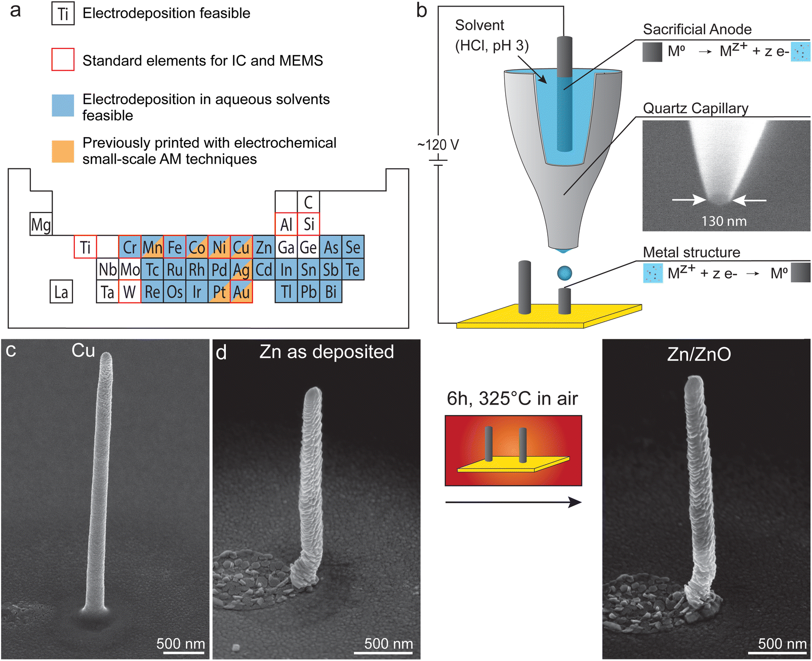 | ||
| Fig. 1 (a) Range of metals that can be electroplated in film form.32 Aqueous solvents allow deposition of many elements that are widely used in integrated circuits or MEMS.7,35 Specifically, a much wider range of metals can be deposited in aqueous solvents than has been printed with EHD-RP and other electrochemical small-scale AM techniques so far.8,33,34 (b) Schematic of the electrohydrodynamic redox-printing (EHD-RP) process. EHD-RP printing is based on the in situ generation of ions and their electrohydrodynamic ejection towards a substrate, driven by an applied DC potential between anode and substrate. Impacting ions are reduced on the substrate, leading to the growth of an out-of-plane structure. Quartz nozzles have orifices in the range of 100–150 nm. The substrates are Au-coated Si wafers. (c) The as-deposited Cu and Zn structures have a minimal feature size of 250 nm (SE SEM micrographs). (d) In a second step, Zn structures can be converted to Zn/Zn oxide core–shell structures by thermal oxidation in air at moderate temperatures (6 h at 325 °C). | ||
In contrast, direct deposition of dense and pure metals can be achieved with electrochemical small-scale AM techniques. Techniques such as meniscus confined electroplating,28,29 electroplating of locally dispensed ions,30 or electrohydrodynamic redox printing (EHD-RP)31 can forgo the need for a post-deposition heat treatment to obtain dense metal structures.23 Unfortunately, a limited range of materials is currently available to these techniques. Traditionally, electrochemical AM techniques have focused on the deposition of Cu and a few other selected metals only, such as Pt and Ag.7 Deposition of non-metallic materials has not yet been reported. However, the small materials range is primarily owed to the relatively recent emergence of these techniques rather than fundamental limitations. A wide range of metals and materials is theoretically accessible to electrochemical methods, as demonstrated by the large number of metals, alloys, and semiconductors that are regularly electroplated in thin- and thick-film form in industry and research32 (Fig. 1a). In principle, electrochemical AM methods must merely translate these results to the local deposition procedures. Indeed, the range of printable metals has been expanded recently. For example, Momotenko et al.33,34 have demonstrated the local 3D deposition of Ni as well as Ni–Mn and Ni–Co alloys with fluidic force microscopy, a technique used for electroplating of locally dispensed ions. While these results are promising, further steps in this direction are needed. Only by expanding the materials palette of electrochemical printing to metals and materials typically used in microfabrication can their benefit of high materials’ quality have a broad impact on the application of these AM methods.
Here we present an approach to increase the range of metals accessible with EHD-RP by using aqueous instead of organic solvents. Recently EHD-RP emerged as an electrochemical AM technique with sub-micron resolution31 (Fig. 1b). EHD-RP utilizes the localized reduction of metal ions to form a metallic deposit on a conductive substrate. The ions are generated in situ, by anodically dissolving a sacrificial electrode immersed in a liquid solvent. Upon impact on the substrate, the ions are reduced to their metallic state, while the solvent evaporates. EHD-RP offers a high printing speed of 10 voxel per s (with minimal voxel sizes of 170 nm), while other electrochemical techniques reach 1–3 voxel per s (with minimal voxel sizes of down to 150 nm).8 Also, EHD-RP is able to modulate the chemistry during printing, thereby enabling multi-metal printing with a chemical feature size of <400 nm. Note that this multi-metal capability is exclusively enabled by the in situ generation of ions from sacrificial anodes. The combination of high-speed printing with multi-metal capability renders EHD-RP a promising toolbox for direct micro-fabrication. However, the use of acetonitrile, an uncommon solvent for standard electrodeposition (but very suitable for electrohydrodynamic ejection), currently limits the range of printable metals. Only Cu and Ag have been printed with high reproducibility,31 and deposition of many other metals failed or was irreproducible.36 In contrast, the use of aqueous solvents would offer higher flexibility. They are widely used for electroplating32 (Fig. 1a) and anodic dissolution of metals in aqueous solvents is well understood.37 Thus, the use of aqueous solvents is highly desirable to access the potential of the widest materials range.
We verify the deposition from aqueous solvents for two model systems, Zn and Cu (Fig. 1c). Also, most importantly in the context of a limited materials range, we show that deposition of metals like Zn opens up a route for the fabrication of metal–oxide structures by post-processing of deposited metal structures (Fig. 1d). Zn in its metallic form is an important material for batteries38,39 and super-capacitors.40 A recent study also showed the fabrication of functional Zn circuits on 3D freeform surfaces.41 ZnO has drawn considerable interest for its electrical properties,42 which render ZnO useful in a wide variety of technical applications, for example in gas sensors,43 ultraviolet light sensors,44 or transistors for flexible electronics.45 An ongoing challenge is the localized manufacturing of such functional structures. By using an automated synthesis tool that allows site-specific, localized deposition such as EHD-RP (and other AM methods), the traditionally used pick-and-place procedure of individual nanowires could be avoided. In contrast to liquid- or vapor-phase growth of nanowires, AM techniques allow for additional control over the shape and orientation of the nanowires. Thus, the change to aqueous solvents outlines a route towards multi-metal and multi-material devices of high quality printed by EHD-RP.
2 Experimental
2.1 Materials
Nozzles for deposition were fabricated on a P-2000 micropipette puller system (Sutter Instruments) from filamented Quartz capillaries (Sutter Instruments, Item QF100-70-15). Pulling parameters were similar to those previously reported.31 The filamented single-channel capillaries were halved in length prior to pulling with a ceramic blade. Nozzle diameters were determined on a Quanta 200F (Thermo Fisher Scientific, former FEI), equipped with a Schottky type field emission gun (FEG) in low vacuum mode (30 Pa) to avoid charging. Nozzles with diameters of 120–200 nm were used for mass spectrometry (MS) experiments and EHD redox printing. The nozzles were filled with the solvent by using gas-tight glass syringes. The nozzles were cleaned on the inside by rinsing with the solvent. Au thin-films on Si wafers were used as substrates. 80 nm thick Au films (3 mTorr Ar, 200 W) were sputtered on top of a 5 nm thick Ti adhesion layer (3 mTorr Ar, 250 W) on (100)-Si wafers (SiMat) in our laboratory sputter facility by DC magnetron sputtering (PVD Products Inc.). The substrates were cut to 0.4 cm × 2.0 cm pieces with a dicing saw. Prior to cutting, a protective layer (MRPL-40, Microresist) was deposited. The protective layer was removed before deposition by ultrasonication in acetone for 5 min and rinsed with isopropanol (both of technical grade). The substrates were subsequently blow-dried with argon. As shown in this and previous work, EHD-RP is compatible with a range of conductive and semiconductive substrates. Zn wires for use as anodes (Alfa Aesar, 0.25 mm diameter, 99.994% metal basis) were etched to remove contamination and surface oxides prior to deposition in diluted HNO3 for 10 s under constant movement to avoid hydrogen bubbles on the wire. The acid was diluted with water (LC/MS-Grade, Fisher Chemical) in a 1![[thin space (1/6-em)]](https://www.rsc.org/images/entities/char_2009.gif) :3 volumetric ratio of 65% HNO3 (Sigma Aldrich) to water to avoid vigorous reaction of the Zn with concentrated nitric acid. Cu wires (Alfa Aesar, 0.25 mm diameter, 99.999% metal basis) were etched in concentrated nitric acid for 10 s. Both wires were subsequently rinsed with deionized water and mounted into the nozzle within 5 minutes from etching. Solvents: 65% HCl and 65% HNO3 (Both Sigma Aldrich) were diluted with water (LC/MS-Grade, Fisher Chemical) to get solutions with pH of 3 and 5.
:3 volumetric ratio of 65% HNO3 (Sigma Aldrich) to water to avoid vigorous reaction of the Zn with concentrated nitric acid. Cu wires (Alfa Aesar, 0.25 mm diameter, 99.999% metal basis) were etched in concentrated nitric acid for 10 s. Both wires were subsequently rinsed with deionized water and mounted into the nozzle within 5 minutes from etching. Solvents: 65% HCl and 65% HNO3 (Both Sigma Aldrich) were diluted with water (LC/MS-Grade, Fisher Chemical) to get solutions with pH of 3 and 5.
2.2 Setup
During deposition, the nozzle is kept stationary above the substrate and brought into focal plane of the optical system with a mechanical uniaxial stage (Z825B, Thorlabs), controlled with a motor controller (Kinesis, Thorlabs), in Y direction and two manual micrometre screws (Mitutoyo) in X and Z direction. The nozzle tip is observed with an optical microscope composed of a ×50 objective lens (LMPLFLN, Olympus) and a CMOS camera (DCC1545M, Thorlabs), illuminated from the opposite side using a green light source (LEDMT1E, Thorlabs). The lens is mounted at an inclination of 60° to the substrate normal. For printing, the substrate is moved by piezo stages in X, Y, and Z direction (QNPXY-500, QNP50Z-250, Ensemble QL controller, Aerotech). Stage translations in X and Y direction larger than 500 μm were enabled by additional long-range stages (M112-1VG, PI for Y direction, manual micrometre screw, Mitutoyo for X direction). A power source (B2962, Keysight) with triaxial cable connectors was used for polarizing the anodes. The metal wire, used as the sacrificial anode in the setup, was connected using a mechanical clamp. Piezo stages and voltage source were controlled through a custom Matlab script. The complete printing setup is mounted on a damped SmartTable (Newport) to provide a vibration-free environment.2.3 Deposition & post-processing
Typical voltages applied to the anode during printing were 110–130 V. Nozzle substrate distance was usually 5–10 μm. Deposition was performed in argon atmosphere (<100 ppm O2, Module ISM-3, Dansensor) under a constant flow of dry argon. No additional heating of the substrate was required during deposition to ensure fast evaporation of the solvent. For post-print oxidation, samples were annealed in a muffle oven (L3/11, Nabertherm) at 325 °C for 6 hours in ambient air (heating rate 2.5° min−1; the cooling rate was not controlled as no active cooling was applied). The samples were placed in an open alumina crucible in the center of the oven. Printed and oxidized samples were stored under vacuum to avoid degradation.2.4 Analysis
Electrospray ionization mass spectrometry (ESI-MS) was performed in positive mode utilizing a hybrid quadrupole time-of-flight (Q-TOF) mass spectrometer (Synapt G2S, Waters). The observed mass range was m/z 50–1000 with 1 s scanning time. A water solution of caesium iodide (99.999%, analytical standard for HR-MS, Fluka) was used as a calibration solution in the declared mass range. The quadrupole profile was set manually to 1. m/z 200, 2. m/z 600, 3. m/z 1000. The subsequent TOF analyser worked in “resolution mode”. Specifically, the most important parameters were: 0.8–1.5 kV capillary voltage, 10 V sampling cone, 0 V source offset, 30 °C source temperature, 2 V trap collision energy, 2 V transfer collision energy, 2 mL min−1 trap gas flow. Scanning electron microscopy (SEM) was performed with a Magellan 400 SEM (Thermo Fisher Scientific, former FEI) equipped with an Octane Super EDXsystem (EDAX, software: Genesis and TEAM, both EDAX). Tilt angles were usually 45 or 55°. HR-SEM images were taken in immersion mode with an acceleration voltage of 5 kV. A dual-beam Helios 5UX (Thermo Fisher Scientific) with a focused Ga+ liquid metal ion source was used for focused ion beam (FIB) milling. Prior to FIB-milling the pillar was coated by a protective carbon layer, which is visible in the transmission electron microscopy (TEM) image as a light grey background. The pillar was subsequently polished from both sides, thereby revealing a vertical cross-section of the pillar. TEM analyses were performed with a Talos F200X TEM (Thermo Fisher Scientific, former FEI) operated at 200 kV in both, TEM and scanning transmission electron microscopy (STEM) imaging modes. STEM signals were recorded using bright field (BF STEM), low-angle annular dark field (LAADF), and high angle annular dark field (HAADF) detectors simultaneously. Photoluminescence spectroscopy (PL) was measured on a Raman microscope (LabRAM HR Evolution UV-VIS-NIR, Horiba) equipped with a He–Cd laser (325 nm, 25 mW, KIMMON) and a 40× UVB objective (Thorlabs LMU-40X UVB). The photoluminescence signal was recorded on a Horiba Synapse EM-CCD while optical microscopy was performed with an IDS uEYE color camera. A grating with 300 g mm−1 was used. The laser power was set to 25%. Artefact peaks in the PL spectra originating from the laser have been subtracted. Spectra of the background and a list with removed peaks are given in the ESI (Fig. S8†)3 Results & discussion
3.1 Deposition from aqueous solvents
Confined deposition of metallic Cu and Zn structures with sub-micron resolution was achieved by using diluted hydrochloric acid as the solvent (Fig. 1c and d). The deposition of Zn was found to depend strongly on the pH of the solvent (Fig. 2a). No confined deposition of Zn was observed from aqueous solvents with neutral pH (pH 7). The addition of a small amount of HCl (pH 5) enabled the deposition of Zn. However, the deposition at pH 5 was characterized by irregular growth rates, which led to Zn pillars varying in size despite each structure was printed with the same deposition parameters (enlarged image in ESI, Fig. S1a†). More homogeneous deposition was achieved with solutions with pH 3. Here, the same deposition parameters for each pillar led to similar heights. A pH lower than three led to a strong reaction of the anode with the solvent, thereby consuming the anode within a short time and precluding any deposition. For Cu, only samples in pH 3 were printed (further images and a comparison to Cu printed with acetonitrile are given in Fig. S2†). | ||
| Fig. 2 (a) Series of SEM micrographs illustrating the effect of solvent pH (adjusted with HCl) on printing performance. The use of ultra-pure water (pH 7) compromised Zn pillar formation. In contrast, a pH of 5 enabled the deposition of Zn, but the deposition is irregular (at invariant deposition parameters, the pillars vary in size, shape, and orientation). Reproducible and confined deposition of Zn was possible when the pH was further reduced to a pH of 3. (b) Electrospray ionization mass spectrometry shows that mainly Zn+ and adducts of Zn with OH and H2O are ejected when diluted HCl (pH 3) is used as a solvent. No compounds containing Cl have been identified. (c) When diluted HNO3 (pH 3) is used, deposition of Zn is irregular. The mass spectra show adducts of Zn and NO3 that can be identified over a broad mass range reaching up to a m/z of 1000. | ||
We used electrospray ionization mass spectrometry (ESI-MS) as a proxy measurement of the ions that are ejected during printing, although with different ejection conditions (namely the voltage and distance between the emitter and counter-electrode). With ESI-MS, Zn ions were identified when a Zn electrode is biased while immersed in water with neutral pH (Fig. S1b†). The mass spectra for solutions with pH 3 (HCl, Fig. 2b) shows mainly adducts of Zn with water and hydroxide. Note that the signal of Zn2+ is absent, as it is out of the range of the instrument. Exchanging HCl for another acid, such as HNO3, yielded an inhomogeneous deposition of Zn (Fig. S3†). Mass spectra for diluted HNO3 (pH 3) shows the presence of species with higher m/z ratios, which are absent for HCl. These patterns can be explained by exact mass identification of different Znx(NO3)y(H2O)z clusters.
In contrast to the results with aqueous solvents, no deposition of Zn was achieved in acetonitrile, the solvent previously used for EHD-RP.31 Moreover, no Zn ions could be identified in ESI-MS when biasing a Zn anode immersed in acetonitrile, indicating that no dissolution takes place at the anode. However, if water is added to the acetonitrile, Zn compounds can be identified after a short time delay (Fig. S4†).
We assume that the formation of Zn ions at the sacrificial anode is the limiting factor in the EHD-RP process. Insolubility of Zn in acetonitrile can be ruled out, as solutions of Zn ions in acetonitrile have been prepared.46 Similarly, a decomposition of the solvent and formation of an inhibiting carbon layer on the anode due to the high applied voltage47 seems unlikely, as addition of water during a running MS experiment enabled formation of Zn ions. A passivating oxide layer on the Zn anode that is insoluble in acetonitrile, but soluble in water, potentially limits the Zn ion formation. Anodic dissolution of Zn in H2O is well known and the Pourbaix diagram of Zn predicts no passivating oxide layer even at neutral pH.48 The low reduction potential of Zn favours the formation of Zn2+ ions over the production of H+ at the sacrificial anode when aqueous solvents are used.49 Yet, despite the identification of Zn ions in the mass spectra, the printing of pure Zn in pH-neutral water was not possible. The high sensibility of ESI-MS presumably detects small amounts of Zn ions that are insufficient for a confined deposition. Since non-volatile compounds other than Zn present in the solvent (such as other metal ions or carbon compounds) are also deposited, the fabrication of pure Zn structures requires the concentration of Zn ions to be significantly higher than these of other species. Another explanation for the clear presence of Zn ions in the mass spectra could be that the higher applied voltage in ESI-MS (1 kV in ESI-MS vs. 100 V in EHD-RP) leads to increased anodic dissolution rate of the Zn wire. However, printing at such high anodic voltages is impractical, as EHD-RP with applied potentials above 200 V leads to unconfined deposition or excessive solvent ejection for our standard working distance of 10 μm.
It is to know that the dissolution rate of Zn increases with decreasing pH of the solvent.50 Indeed, the addition of HCl in printing experiments enabled the deposition of Zn. No chloride ions could be identified in the mass spectra when HCl was added to the solvent. Since the mass spectra were taken in positive mode, the absence of anions can not be excluded completely. In contrast to HCl, however, nitrate ions were found when nitric acid was added. The presence of nitrate anions could explain why the deposition from nitrate containing solutions was inhomogeneous, with variations in both the morphology and the oxygen content of individual pillars (Fig. S3†). A decomposition of NO3− on the substrate could lead to precipitation of ZnO.51 While this may open an approach for the direct deposition of ZnO, the irregular deposition and absence of spatial confinement preclude the use of HNO3 for the deposition of pure Zn. In summary, these findings show that confined printing of metals can be achieved by using diluted acids as solvents and that the nature of the acid is important to the deposition of pure metal structures.
3.2 As-deposited, metallic Zn
Fig. 3a shows a scanning electron micrograph of an as-deposited Zn pillar, printed from diluted HCl (pH 3). The pillar has a width of 250 nm. Additionally, a ring-like feature is often visible around printed pillars (also clearly visible in pillar arrays, such as in Fig. 2a). Energy dispersive X-ray (EDX) analysis of a pillar (Fig. 3b) indicates that only small amounts of carbon and oxygen were present in the as-deposited state. Carbon and oxygen can be artifacts from the SEM analysis itself and are found regularly in printed structures.31 A native oxide layer will also generate an oxygen signal, as the samples have been exposed to air prior to SEM analysis. In general, the low oxygen signal indicates that most of the hydroxide and water that formed adducts with Zn ions in mass spectrometry are not incorporated into the structure. The Au-signal around 2.2 keV arises from the substrate. Notably, no Cl signal was detected, which matches the results from ESI-MS.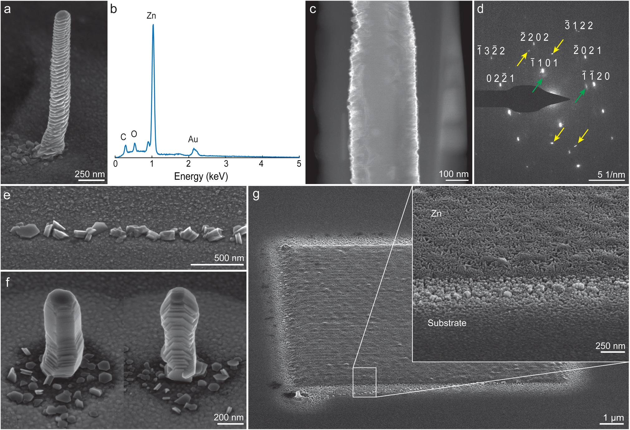 | ||
| Fig. 3 As-deposited Zn structures. (a) Zn pillar (b) corresponding energy-dispersive X-ray (EDX) spectrum, taken in spot modus on the pillar itself. The C–K and O–K peaks likely originate from contamination originating from either printing or SEM analysis. The Au signal originates from the substrate. (c) A TEM cross-section of a pillar shows a dense structure as printed. (d) Selected area electron diffraction indicates single-crystal-like Zn, with the presence of a small amount of epitaxial Zn oxide (green arrows). Additional reflexes (yellow arrows) indicate the presence of Zn grains with a different orientation (Fig. S5†). (e) Printing with a high translation speed of the nozzle arrests deposition after nucleation (vstage = 8 μm s−1). The individual nuclei that form on the Au substrate are of random crystallographic orientation. (f) Due to randomly oriented nucleation, different pillars exhibit different crystallographic orientations. (g) Deposition in a layer-by-layer mode, such as for the shown 10 by 10 μm square (hatch distance: 100 nm), results in a different surface morphology without preferred crystal orientation. All shown structures in a–g were printed with pH 3 (HCl), except f, which was printed with pH 5 (HCl). | ||
All deposited Zn pillars showed a pronounced surface structure, resembling basal-plane stacked hexagonal platelets. The orientation (i.e., the tilt of the basal plane of the hexagonal platelets with respect to the substrate) of these platelets was constant along the length of an individual pillar. The observed surface morphology fits with the expected crystallographic hexagonal close packed (HCP) structure of metallic Zn (space group P63/mmc). A cross-section, imaged in a transmission electron microscopy (TEM), reveals an as-printed dense microstructure (Fig. 3c, additional images in Fig. S5†). Electron diffraction (Fig. 3d) verified a crystalline, textured structure that fits a Zn lattice. The second set of spots observed with some reflexes (indicated with green arrows) probably indicate an epitaxial ZnO layer.52 Additional spots (yellow arrows) that fit neither patterns suggest that the specimen was not single crystalline. The most probable origin is a Zn grain with a different crystallographic orientation.
The orientation of Zn nuclei was found to be random (Fig. 3e). For the presented experiment, the growth of Zn was limited by translating the substrate at a high speed, resulting in a short residence time of the nozzle over a specific site (vstage = 8 μm s−1, corresponding to a residence time of 1.6 × 10⁻² s over the length of a typical nozzle orifice diameter). As shown in Fig. 3f, this random nucleation led to different orientations between individual pillars.
Layer-by-layer deposition refined the surface morphology. Fig. 3g shows a 10 by 10 μm Zn square (hatch distance: 100 nm) deposited in five overpasses. The structure appeared to comprise randomly oriented platelets with visible porosity in SEM micrographs. The layer-by-layer printing probably avoids preferred growth of a specific nuclei and leads to a polycrystalline, randomly oriented microstructure.
We always observed a layered growth when individual zinc pillars were printed. In contrast, the morphology of zinc electroplated in thin-film form depends on the current densities.39,53 The morphology changes with increasing current density from mossy to layered, to large grains and at high current densities to dendritic Zn deposition, governed by a change from a reaction-limited deposition to a diffusion-limited growth.53 Layered growth, as observed in our experiments, is generally reported for moderate current densities of <100 mA cm−2.39 The current densities during our experiments were estimated to be higher, that is, approximately 0.6–1.8 A cm−2 (a printing current of 0.3–0.9 nA was measured for a pillar with 250 nm diameter). The fact that we observe layered growth at somewhat higher estimated current densities than previously reported for standard electroplating might arise from the nature of the printing process. EHD-RP is characterized by the forced transport of ions and the confined nature of the deposition within droplets which results in short diffusion paths. This could lead to a reaction-limited deposition, despite high current densities.
Another observed difference to the deposition of thin films is the evolution of texture. In thin films, layered growth typically results in competitive evolution of a specific texture. The favoured growth direction of Zn crystals is along the [0001] direction of the platelets.39 Hence, the printed pillars should grow preferably along the [0001] direction. In printed pillars, however, we observe a random variation between the texture and the growth direction. This could be explained by a combination of peculiarities in nucleation and growth in EHD-RP. Often multiple nuclei are visible with random orientation (Fig. 3e). We assume that during initial plating stages, a solvent droplet resides on the surface, in which multiple nuclei are formed. In electroplating of thin films, Zn is known to nucleate with random orientation at high overpotentials, but also in the presence of contaminants.54 The current EHD-RP process unfortunately precludes a measurement of the precise surface potential during the deposition. Nevertheless, the applied potential of 120 V implies a high overpotential, which would explain the random nucleation. Subsequent to nucleation, a single nucleus is selected to grow fastest. This selection is influenced by other factors than the crystallographic orientation of the nucleus, but could be based on the field-focusing effect.55 This effect would cause the highest protrusion to grow preferably. While the orientation of the initial nucleus defines the crystallographic orientation of the printed structure, it does not define the growth direction in EHD-RP. The growth direction is strictly given by directional drop-by-drop addition of material by the printing process. The misalignment of the [0001] axis and the forced out-of-plane growth direction of the pillars gives rise to the terraced appearance of the surface, as successive layers are shifted to match the crystal growth direction with the growth direction given by EHD-RP. The ring-like feature, that is often observed around pillars, might arise from the deposition of uncharged material, which is not deposited in a confined manner due to the absence of field-focusing for uncharged species.
3.3 Partial thermal conversion of Zn structures to ZnO
The deposited Zn structures were thermally oxidized in air to form a metal–oxide. Fig. 4a shows an individual pillar after oxidation. The surface morphology, resembling stacked hexagonal platelets, was still visible. A comparison of an as-deposited array with an array after oxidation at 325 °C for 6 h is shown in Fig. 4b and c. In the shown arrays, most pillars appeared inclined after oxidation, while around 10% tip over completely. A closer inspection showed that the tipped pillars failed at the interface to the substrate. A reduction in oxidation temperature to 250 °C and 300 °C has not reduced tilting of the pillars during oxidation (Fig. S7†). Conversion to ZnO at 325 °C for 6 h, however, was not complete. | ||
| Fig. 4 Thermally oxidized Zn structures. (a) An oxidized pillar. (b and c) A comparison of an array in the as-deposited state and after oxidation. (d) Direct comparison of a pillar in the as-deposited state and after oxidation. A volume increase can be seen. (e) A cross-section of a pillar after thermal oxidation, imaged in TEM using a high-angle annular dark-field detector. (f) Zoomed-in image of the base of the pillar with corresponding elemental analysis maps. An oxide-rich shell is formed around a core containing mostly Zn. (g) Electron diffraction, taken on the pillar shown in (e), shows spots originating from ZnO with wurtzite structure but also from metallic Zn. This shows the presence of an metallic Zn core. (h) EDX analysis, carried out in a SEM, shows a significant increase in oxygen level during oxidation. (i) Photoluminescence spectra shows almost no signal in the as printed state, while the same structure yields a strong signal after oxidation with a peak around 390 nm. | ||
The observed tilting of the pillars during oxidation could be caused by a weak interface between pillar and substrate, for example due to pores, such as observed in Fig. 4e. Similarly, SEM images of cross sections of as-printed pillars of Zn (in HNO3, Fig. S3g†) and Cu (Fig. S2d†) exhibit pores at the interface to the substrate. Such pores could be a consequence of hydrogen gas formation during initial plating stages of a metallic pillar,56 while in later printing stages either less hydrogen is formed or it is not trapped in the structure. While previous studies of the mechanical properties of metals printed by EHD-RP showed high density and mechanical strength,23 the here-observed porosity will naturally negatively affect not only the behaviour during oxidation but also mechanical and electrical properties.
A first hint towards incomplete oxidation came from a comparison of the pillar volume in the as-printed and post-oxidation state. The SE micrographs indicated an approximate volume increase of 20% upon oxidation (Fig. 4d and Fig. S6†), while the difference in the unit cells of Zn and ZnO predicts a volume increase of 60%. Incomplete oxidation with the presence of an oxide shell and a Zn-rich core was clearly indicated by a region of lower brightness at the surface of an oxidized pillar in a high angle annular dark field mode (HAADF) TEM micrograph (Fig. 4e). The low contrast towards the tip of the pillar can most probably be attributed to a decreasing thickness of the lamella itself. An image of the base of the pillar with higher magnification and corresponding EDX Maps of the same area for the Zn–K and O–K signal are shown in Fig. 4f. An overlay of the two maps showed a higher oxygen content in the area having a low contrast in the HAADF image, indicating an oxygen-rich shell around a core containing mostly Zn. Fig. 4g shows an electron diffraction pattern after oxidation, taken on the pillar shown in Fig. 4e. Importantly, reflexes of both, metallic Zn and ZnO (wurtzite structure) can be identified, underscoring the two-phase nature of the partially oxidized pillar. EDX analysis after oxidation (Fig. 4h), taken in SEM on an unpolished pillar, gives an estimated Zn to O ratio of 1.2, while stoichiometric ZnO would have a ratio of 1. This result, however, should be treated as an approximation because of the limited quantitative accuracy of EDX for low atomic number elements.
The incomplete oxidation and formation of ZnO shells has been reported for oxidation at temperatures as low as 110 °C (ref. 57) and with increasing oxide shell thickness for higher temperatures. We have chosen 325 °C as a compromise between thin oxide layers and the surface restructuring and whisker formation reported at higher temperatures that can compromise shape retention of the deposited structure.52,58
Despite the incomplete oxidation, semiconducting properties of the ZnO shell are clearly evident. Photoluminescence (PL) spectrometry was performed before and after thermal treatment (Fig. 4i) to study these properties. The PL spectra were taken at room temperature in ambient air. For the as-deposited state, a weak signal with a peak at 375 nm is found. This signal can be attributed to transitions in metallic Zn from a sp conduction band near the Fermi surface to the valence band (3d band).52 The PL spectra changed significantly upon oxidation with an intense signal peaking at 390 nm and a broad emission above 450 nm detected, respectively. The signal at 390 nm can be attributed to band-edge emission of ZnO and correlates to a bandgap of 3.18 eV. This values is 0.05 eV smaller than the reported bandgap of ZnO of 3.23 eV measured with PL.59 However, the precise position of the maximum reported in the literature depends on the temperature during PL measurement, the shape of structures, and near-edge level states created by defects and impurities.59 The broad emission above 450 nm is related to defects and/or impurities.60,61
4 Conclusions
In summary, we have presented an approach for the additive manufacturing of Zn and ZnO structures with minimal feature sizes of 250 nm using EHD-RP. Mass spectrometry indicates that diluted hydrochloric acid is a suitable solvent for the deposition of Zn and Cu. Homogeneous deposition was achieved using a solvent with pH 3. The deposited Zn features a dense, crystalline microstructure and shows pronounced crystal facets on the surface. Still, further experiments are necessary to address the observed porosity at the interface to the substrate and towards the long-term stability of the Zn structures. The Zn can be partially converted into semiconducting ZnO by thermal oxidation, as shown with cross-sections of pillars after oxidation. Photoluminescence spectroscopy confirmed the transformation from Zn to ZnO. Here, a future parametric study of the process might reveal optimized conditions for the oxidation. Namely, the temperature, heating rate and the duration of the oxidation have to be addressed. The here-presented work lays the foundation for future work that will investigate properties of the formed Zn/ZnO such as the electrical and mechanical properties and outlines the use of direct, site-specific synthesis of functional materials by AM for future use in demonstrator devices such as gas sensors. In general, the shown compatibility of EHD-RP with aqueous solvents could enable to the deposition of various metals, as an extensive range of metals can be dissolved and re-deposited in such solvents. In addition, the absence of chlorine ions in the mass spectra as well as in EDX measurements indicates that aqueous metal salt solutions are an alternative to the sacrificial anode as ion sources. The use of metal salts instead of sacrificial anodes could grant access to the deposition of more noble metals, which do not corrode readily in aqueous solvents.Author contributions
M. N., A. R. and R. S. devised the concept. R. S. and A. R. supervised the project. M. N. performed deposition experiments. M. N. and A. R. provided SEM and FIB analysis. A. P. and M. N. performed MS experiments in the laboratory of R. Z. and performed MS data analysis. A. R., M. N., H. G. and R. S. validated the results on a regular basis, while all authors discussed the results. M. N. wrote the original paper draft and visualised the data. All authors reviewed and commented on the draft.Conflicts of interest
The Authors declare no conflicts of interest.Acknowledgements
The authors thank J. Sendra, N. Porenta (both Laboratory for Nanometallurgy, ETH Zürich) and A. Sologubenko (ScopeM, ETH Zürich) for experimental support with photoluminescence spectroscopy and TEM analysis, respectively. The authors thank M. Menétrey for fabricating the substrates. The authors gratefully thank D. Momotenko (Laboratory of Biosensors and Bioelectronics, ETH Zürich) for access to the nozzle-puller. This work was funded by Grant No. SNF 200021-188491 and partially supported by Grant No. SNF 200020-178765. Electron-microscopy analysis was performed at ScopeM, the microscopy platform of ETH Zürich.References
- I. Gibson, D. Rosen and B. Stucker, Additive manufacturing technologies: 3D printing, rapid prototyping and direct digital manufacturing, Springer New York Heidelberg Dordrecht London, 2015 Search PubMed.
- M. J. Madou, Fundamentals of Microfabrication and Nanotechnology, CRC Press, 3rd edn, 2011, p. 1992 Search PubMed.
- MEMS Materials and Processes Handbook, ed. R. Ghodssi and P. Lin, Springer US, Boston, MA, 2011 Search PubMed.
- P. Golvari and S. M. Kuebler, Micromachines, 2021, 12, 1–24 CrossRef PubMed.
- X. Wen, B. Zhang, W. Wang, F. Ye, S. Yue, H. Guo, G. Gao, Y. Zhao, Q. Fang, C. Nguyen, X. Zhang, J. Bao, J. T. Robinson, P. M. Ajayan and J. Lou, Nat. Mater., 2021, 20, 1506–1511 CrossRef CAS PubMed.
- F. Rajabasadi, L. Schwarz, M. Medina-Sánchez and O. G. Schmidt, Prog. Mater. Sci., 2021, 120, 100808 CrossRef CAS.
- L. Hirt, A. Reiser, R. Spolenak and T. Zambelli, Adv. Mater., 2017, 29, 1604211 CrossRef PubMed.
- J. Hengsteler, G. P. S. Lau, T. Zambelli and D. Momotenko, Electrochem. Sci. Adv., 2021, 1–14 Search PubMed.
- M. Carlotti and V. Mattoli, Small, 2019, 15, 1–22 CrossRef PubMed.
- S. Kumar, P. Bhushan, M. Pandey and S. Bhattacharya, J. Micro Nanomanuf., 2019, 2, 175–197 Search PubMed.
- G. D. Pasquale, Micromachines, 2021, 12, 1374 CrossRef PubMed.
- A. E. Jakus, S. L. Taylor, N. R. Geisendorfer, D. C. Dunand and R. N. Shah, Adv. Funct. Mater., 2015, 25, 6985–6995 CrossRef CAS.
- H. J. Kwon, J. Hong, S. Y. Nam, H. H. Choi, X. Li, Y. J. Jeong and S. H. Kim, Mater. Adv., 2021, 2, 5593–5615 RSC.
- P. Serra and A. Piqué, Adv. Mater. Technol., 2019, 4, 1–33 CrossRef.
- E. L. Papadopoulou, E. Axente, E. Magoulakis, C. Fotakis and P. A. Loukakos, Appl. Surf. Sci., 2010, 257, 508–511 CrossRef CAS.
- M. Feinaeugle, R. Pohl, T. Bor, T. Vaneker and G. w. Römer, Addit. Manuf., 2018, 24, 391–399 CAS.
- Y. L. Kong, I. A. Tamargo, H. Kim, B. N. Johnson, M. K. Gupta, T. W. Koh, H. A. Chin, D. A. Steingart, B. P. Rand and M. C. McAlpine, Nano Lett., 2014, 14, 7017–7023 CrossRef CAS PubMed.
- H. Kim, R. C. Auyeung and A. Piqué, J. Power Sources, 2007, 165, 413–419 CrossRef CAS.
- K. Sun, T. S. Wei, B. Y. Ahn, J. Y. Seo, S. J. Dillon and J. A. Lewis, Adv. Mater., 2013, 25, 4539–4543 CrossRef CAS PubMed.
- S. Y. Kim, K. Kim, Y. H. Hwang, J. Park, J. Jang, Y. Nam, Y. Kang, M. Kim, H. J. Park, Z. Lee, J. Choi, Y. Kim, S. Jeong, B. S. Bae and J. U. Park, Nanoscale, 2016, 8, 17113–17121 RSC.
- D. W. Yee, M. L. Lifson, B. W. Edwards and J. R. Greer, Adv. Mater., 2019, 31, 1–9 CrossRef PubMed.
- A. Vyatskikh, S. Delalande, A. Kudo, X. Zhang, C. M. Portela and J. R. Greer, Nat. Commun., 2018, 9, 593 CrossRef PubMed.
- A. Reiser, L. Koch, K. A. Dunn, T. Matsuura, F. Iwata, O. Fogel, Z. Kotler, N. Zhou, K. Charipar, A. Piqué, P. Rohner, D. Poulikakos, S. Lee, S. K. Seol, I. Utke, C. van Nisselroy, T. Zambelli, J. M. Wheeler and R. Spolenak, Adv. Funct. Mater., 2020, 30, 1–20 CrossRef PubMed.
- J. Schneider, P. Rohner, D. Thureja, M. Schmid, P. Galliker and D. Poulikakos, Adv. Funct. Mater., 2016, 26, 833–840 CrossRef CAS.
- R. Winkler, J. D. Fowlkes, P. D. Rack and H. Plank, J. Appl. Phys., 2019, 125, 210901 CrossRef.
- I. Utke, P. Hoffmann and J. Melngailis, J. Vac. Sci. Technol., B: Microelectron. Nanometer Struct. – Process., Meas., Phenom., 2008, 26, 1197 CrossRef CAS.
- A. Botman, J. J. Mulders and C. W. Hagen, Nanotechnology, 2009, 20, 372001 CrossRef CAS PubMed.
- J. Hu and M. F. Yu, Science, 2010, 329, 313–316 CrossRef CAS PubMed.
- J. Hengsteler, B. Mandal, C. Van Nisselroy, G. P. Lau, T. Schlotter, T. Zambelli and D. Momotenko, Nano Lett., 2021, 21, 9093–9101 CrossRef CAS PubMed.
- L. Hirt, S. Ihle, Z. Pan, L. Dorwling-Carter, A. Reiser, J. M. Wheeler, R. Spolenak, J. Vörös and T. Zambelli, Adv. Mater., 2016, 28, 2311–2315 CrossRef CAS PubMed.
- A. Reiser, M. Lindén, P. Rohner, A. Marchand, H. Galinski, A. S. Sologubenko, J. M. Wheeler, R. Zenobi, D. Poulikakos and R. Spolenak, Nat. Commun., 2019, 10, 1–8 CrossRef CAS PubMed.
- Modern Electroplating, ed. M. Schlesinger and M. Paunovic, John Wiley & Sons, Inc., Hoboken, NJ, 5th edn, 2011 Search PubMed.
- C. van Nisselroy, C. Shen, T. Zambelli and D. Momotenko, Addit. Manuf., 2021, 53, 102718 Search PubMed.
- C. Shen, Z. Zhu, D. Zhu, C. v. Nisselroy, T. Zambelli and D. Momotenko, Nanotechnology, 2022, 33, 265301 CrossRef PubMed.
- M. Schwartz, Handbook of Deposition Technologies for Films and Coatings—Science, Technology and Applications, Elsevier Inc., Kidlington, Oxford, UK, 3rd edn, 2010, pp. 506–616 Search PubMed.
- A. Reiser, Ph.D. thesis, ETH Zürich, 2019.
- E. McCafferty, Introduction to Corrosion Science, Springer New York, New York, NY, 2010 Search PubMed.
- L. Cao, D. Li, T. Pollard, T. Deng, B. Zhang, C. Yang, L. Chen, J. Vatamanu, E. Hu, M. J. Hourwitz, L. Ma, M. Ding, Q. Li, S. Hou, K. Gaskell, J. T. Fourkas, X. Q. Yang, K. Xu, O. Borodin and C. Wang, Nat. Nanotechnol., 2021, 16, 902–910 CrossRef CAS PubMed.
- V. Jabbari, T. Foroozan and R. Shahbazian-Yassar, Adv. Energy Sustain. Res., 2021, 2, 2000082 CrossRef.
- P. Zhang, Y. Li, G. Wang, F. Wang, S. Yang, F. Zhu, X. Zhuang, O. G. Schmidt and X. Feng, Adv. Mater., 2019, 31, 1806005 CrossRef PubMed.
- N. Yi, Y. Gao, A. Lo Verso, J. Zhu, D. Erdely, C. Xue, R. Lavelle and H. Cheng, Mater. Today, 2021, 50, 24–34 CrossRef CAS PubMed.
- A. B. Djuriić, A. M. Ng and X. Y. Chen, Prog. Quantum Electron., 2010, 34, 191–259 CrossRef.
- M. N. Cardoza-Contreras, J. M. Romo-Herrera, L. A. Ríos, R. García-Gutiérrez, T. A. Zepeda and O. E. Contreras, Sensors, 2015, 15, 30539–30544 CrossRef CAS PubMed.
- Y. K. Su, S. M. Peng, L. W. Ji, C. Z. Wu, W. B. Cheng and C. H. Liu, Langmuir, 2010, 26, 603–606 CrossRef CAS PubMed.
- L. Jiang, J. Li, K. Huang, S. Li, Q. Wang, Z. Sun, T. Mei, J. Wang, L. Zhang, N. Wang and X. Wang, ACS Omega, 2017, 2, 8990–8996 CrossRef CAS PubMed.
- P. D'Angelo and V. Migliorati, J. Phys. Chem. B, 2015, 119, 4061–4067 CrossRef PubMed.
- S. Bia and E. T. Bandura, Electrochim. Acta, 1987, 32, 891–894 CrossRef.
- B. Beverskog and I. Puigdomenech, Corros. Sci., 1997, 39, 107–114 CrossRef CAS.
- A. T. Blades, M. G. Ikonomou and P. Kebarle, Anal. Chem., 1991, 63, 2109–2114 CrossRef CAS.
- X. G. Zhang, Corrosion and Electrochemistry of Zinc, Springer Science+Business Media New York, 1996 Search PubMed.
- S. Jiao, K. Zhang, S. Bai, H. Li, S. Gao, H. Li, J. Wang, Q. Yu, F. Guo and L. Zhao, Electrochim. Acta, 2013, 111, 64–70 CrossRef CAS.
- H. S. Chou, K. D. Yang, S. H. Xiao, R. A. Patil, C. C. Lai, W. C. V. Yeh, C. H. Ho, Y. Liou and Y. R. Ma, Nanoscale, 2019, 11, 13385–13396 RSC.
- R. Y. Wang, D. W. Kirk and G. X. Zhang, J. Electrochem. Soc., 2006, 153, C357–C364 CrossRef CAS.
- A. Khor, P. Leung, M. R. Mohamed, C. Flox, Q. Xu, L. An, R. G. Wills, J. R. Morante and A. A. Shah, Mater. Today Energy, 2018, 8, 80–108 CrossRef.
- P. Galliker, J. Schneider, H. Eghlidi, S. Kress, V. Sandoghdar and D. Poulikakos, Nat. Commun., 2012, 3, 1–9 Search PubMed.
- J. Stevanović, S. Gojković, A. Despić, M. Obradović and V. Nakić, Electrochim. Acta, 1997, 43, 705–711 CrossRef.
- R. Nakamura, J. G. Lee, D. Tokozakura, H. Mori and H. Nakajima, Mater. Lett., 2007, 61, 1060–1063 CrossRef CAS.
- X. Ma and M. R. Zachariah, J. Phys. Chem. C, 2009, 113, 14644–14650 CrossRef CAS.
- A. B. Djurišić and Y. H. Leung, Small, 2006, 2, 944–961 CrossRef PubMed.
- V. Srikant and D. R. Clarke, J. Appl. Phys., 1998, 83, 5447–5451 CrossRef CAS.
- H. Zeng, G. Duan, Y. Li, S. Yang, X. Xu and W. Cai, Adv. Funct. Mater., 2010, 20, 561–572 CrossRef CAS.
Footnote |
| † Electronic supplementary information (ESI) available. See DOI: https://doi.org/10.1039/d2nr04549d |
| This journal is © The Royal Society of Chemistry 2022 |