Ionic dielectrics for fully printed carbon nanotube transistors: impact of composition and induced stresses

Brittany N. Smith a, Hope Meikle ab, James L. Doherty a, Shiheng Lu a, Gianna Tutoni b, Matthew L. Becker b, Michael J. Therien b and Aaron D. Franklin *ab
aDepartment of Electrical and Computer Engineering, Duke University, Durham, NC 27708, USA. E-mail: aaron.franklin@duke.edu; Tel: +1-919-681-9471
bDepartment of Chemistry, Duke University, Durham, NC 27708, USA

Received 29th July 2022 , Accepted 31st October 2022

First published on 4th November 2022


Abstract

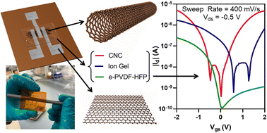
Printed carbon nanotube thin-film transistors (CNT-TFTs) are candidates for flexible electronics with printability on a wide range of substrates. Among the layers comprising a CNT-TFT, the gate dielectric has proven most difficult to additively print owing to challenges in film uniformity, thickness, and post-processing requirements. Printed ionic dielectrics show promise for addressing these issues and yielding devices that operate at low voltages thanks to their high-capacitance electric double layers. However, the printing of ionic dielectrics in their various compositions is not well understood, nor is the impact of certain stresses on these materials. In this work, we studied three compositionally distinct ionic dielectrics in fully printed CNT-TFTs: the polar-fluorinated polymer elastomer PVDF-HFP; an ion gel consisting of triblock polymer PS-PMMA-PS and ionic liquid EMIM-TFSI; and crystalline nanocellulose (CNC) with a salt concentration of 0.05%. Although ion gel has been thoroughly studied, e-PVDF-HFP and CNC printing are relatively new and this study provides insights into their ink formulation, print processing, and performance as gate dielectrics. Using a consistent aerosol jet printing approach, each ionic dielectric was printed into similar CNT-TFTs, allowing for direct comparison through extensive characterization, including mechanical and electrical stress tests. The ionic dielectrics were found to have distinct operational dependencies based on their compositional and ionic attributes. Overall, the results reveal a number of trade-offs that must be managed when selecting a printable ionic dielectric, with CNC showing the strongest performance for low-voltage operation but the ion gel and elastomer exhibiting better stability under bias and mechanical stresses.


1. Introduction

Printed electronics have the potential to transform the growing internet of things (IoT) by offering customizability for a wide range of applications at low cost.1–3 Material selection for printed devices is a leading factor in determining performance and suitability for application needs.4–6 For instance, printed networks of semiconducting single-walled carbon nanotubes (CNTs) have proven to be highly versatile, enabling a diverse assortment of printed thin-film transistors (TFTs) operating as biosensors,7 pressure sensors,8 backplane displays,9,10 and logic gates.11 Without the need for harsh post-processing treatments, flexible substrates such as Kapton,12–14 PDMS,11 PET,15,16 and paper,17 have been utilized for printed CNT-TFTs. As fully printed, flexible CNT-TFTs have advanced, it has become increasingly evident that the gate dielectrics not only play a crucial role in realizing high-performance devices but are also one of the most difficult layers to print additively and achieve strong gate control at reasonably low voltages (sub-5 V). While insulating materials, such as hexagonal boron nitride (hBN), have proven useful in fully print-in-place CNT-TFTs, these 2D nanomaterials form thin films that are microns thick and require several tens of volts to effectively modulate the semiconducting CNT thin-film channel.18 Regardless of whether the semiconducting channel for a fully printed TFT is of CNTs, a 2D semiconductor such as MoS2,19,20 or an organic semiconductor,21–23 the printed gate dielectric must be solution processable, maintain stable performance under mechanical bending, and have a high gate capacitance for low-voltage operation.24

Ionic dielectrics, also known as electrolyte dielectrics, are strong candidates for printed transistors due to their potential compatibility with solution-phase dispersion into inks and exceptionally high capacitance from the formation of electric double layers (EDLs). Simply put, ionic dielectrics are composed of ions in a material that supports ionic conduction. Many compositional variations of ionic dielectrics have been successfully demonstrated in TFTs with semiconducting channels of organic semiconductors,25–27 2D materials,28–30 or CNTs.31,32 Each ionic dielectric has a thickness-independent capacitance due to EDL formation at the dielectric/channel and dielectric/electrode interfaces. These EDLs are formed by the conduction of ions in the material as they are coulombically attracted to their respective dielectric interface under an applied gate potential. Because the EDLs form abruptly at the dielectric interfaces, the resultant capacitance is exceptionally high, allowing for low operating voltage when used as the gate dielectric for a TFT.33–35

While ionic dielectrics offer attractive features, there are challenges to using these materials for printed, flexible transistors. Reliance on ion transport limits the switching speed for the devices, which hampers their suitability for applications that require even modest operating frequencies.36 Depending on the composition of the ionic dielectric, as well as the gate electrode and semiconducting channel, there is potential for electrochemical reactivity at the interfaces that can result in material decomposition and/or excessive gate leakage currents, particularly when under extended bias stress.37–39 Given the large variety of material compositions for ionic dielectrics,40 there is uncertainty regarding how different compositions influence core ionic properties and, correspondingly, performance as a printed gate dielectric. What is clear is that the multitude of individual demonstrations of ionic dielectrics in printed TFTs have not identified the role that film composition plays in ultimate performance and stability.

In this study, we developed a flexible CNT-TFT device platform having broad compatibility with printed dielectrics and used the platform to study three distinct ionic dielectrics: a custom-developed crystalline nanocellulose (CNC), an elastomeric poly(vinylidene fluoride-co-hexafluoropropylene) (PVDF-HFP), and an ion gel based on polystyrene-b-methyl methacrylate-b-styrene (PS-PMMA-PS) and 1-ethyl-3-methylimidazolium bis(trifluoro-methylsulfonyl)imide (EMIM-TFSI). Since e-PVDF-HFP and CNC printing are still in their infancy, this study provides insights into their aerosol jet printing optimization, working mechanisms, and their respective strengths and weaknesses as printed gate dielectrics. Key trade-offs and potential applications for these novel printable materials are identified. Because ionic dielectrics are performance-limited by ionic diffusion, the impact of voltage sweep rate on switching characteristics was directly compared, showing CNC devices have strong performance retention up to a sweep rate of 40 V s−1. Further, electrical bias stress testing was completed over 12 hours, during which ion gel devices yielded the best stability. Additionally, mechanical stress testing was carried out to examine the flexibility of these TFTs, which demonstrated that devices with ion gel and e-PVDF-HFP dielectrics remained stable through 1000 bending cycles. This extensive evaluation of three printed ionic dielectrics provides insights into their operation, compositional-dependence, and limitations for use in fully printed CNT-TFTs.

2. Results and discussion

2.1. Diverse compositions of ionic dielectrics for CNT-TFTs

The selection of the three ionic dielectrics for this work was made by choosing two materials from the most prominent classifications of ionic dielectrics and a third material that has recently shown promise as an environmentally friendly dielectric. First, ion gels, which are among the most popular ionic dielectric subclasses, consist of a mixture of a block copolymer and an ionic liquid in varying ratios, often with specific capacitances up to 10 μF cm−2.41–43 In most ion gels, the polymer is a self-assembled triblock copolymer that allows for gelation to occur at low polymer weight fractions, which is optimal for compatibility with printing techniques that require low ink viscosities.44 Many copolymers have been explored for ion gels, including PS-PEO-PS,26,44 PS-PMMA-PS,12 SOS,45 and SEAS.46,47 Ionic liquids, which often make up a larger weight percentage of the ion gel than the copolymer, provide the high concentration of ions that form the EDL. Commonly used ionic liquids for ion-gel formulations include EMIM-TFSI, BMIM-PF6, and EMIM-OctOSO3.48 The combination of PS-PMMA-PS and EMIM-TFSI in a range of ratios has shown high maximum operating frequencies, capacitances, and compatibility with many semiconducting materials, including graphene,29,49 MoS2,50 and organic semiconductors.51–53 Recently, a fully aerosol jet printed CNT-TFT composed of a 1[thin space (1/6-em)]:[thin space (1/6-em)]9 w/w ratio of PS-PMMA-PS to EMIM-TFSI was demonstrated with high electrical and mechanical stability at a low device operating voltage of 1 V.12 Hence, for this study we focused on the same formulation.

In ion gels, the ions are contributed from an ionic liquid and tend to cause high gate leakage currents through the device, thus reducing TFT performance. To reduce the concentration of ions in the material while maintaining low device operating voltages, elastomers – another subclass of ionic dielectrics – have also been studied for TFTs. Elastomers have orders of magnitude smaller concentrations of mobile ions than ion gels yet are also able to form EDLs under small, applied voltages due to their low glass transition temperature (Tg).54 Some elastomers that have been explored include PMMA, PDMS, PU, and SBS.54 A more recently studied material is the elastomer poly(vinylidene fluoride-co-hexafluoropropylene) (e-PVDF-HFP), which is elastic and has a low Tg due to its high stoichiometric ratio of HFP monomers.55 The e-PVDF-HFP dielectric acquires ions through impurities on the substrate, in its solvent, or by additives. e-PVDF-HFP was recently utilized as the gate dielectric for an inkjet printed CNT-TFT and showed decent device performance at a 1 V operating voltage.56 A new formulation of e-PVDF-HFP was developed for this study, making the ink compatible with aerosol jet printing.

Given that ionic dielectric inks are typically composed of hazardous materials and utilize harsh solvents, a push to use environmentally safe materials has led to the recent demonstration of CNC, a water-soluble carbon-based insulator, in a CNT-TFT with low operating voltages.17 With the addition of sodium chloride (NaCl) to the CNC, the dielectric performance improved and faster voltage sweep rates were realized without compromising device performance. However, a more complete understanding of the operation and limits to the use of CNC as a printed ionic dielectric is lacking. Hence, the third ionic dielectric selected and optimized for this work was an aqueous CNC ink.

There are three key design features that enabled broad compatibility of the flexible CNT-TFT platform with these diverse ionic dielectrics: a Kapton substrate, graphene electrodes, and a top-gate configuration. First, all CNT-TFTs were aerosol jet printed on a Kapton substrate that was pre-treated with KOH for 3 minutes to improve hydrophilicity, which provides a flexible non-porous surface to support both ion gels and CNC. Secondly, while side-gating is possible with ion gels to reduce process steps, a top-gate design was chosen to support elastomers, which exhibit lower capacitances than ion gels. Thirdly, graphene source/drain/gate electrodes were utilized due to the top-gate electrode requirement of a room temperature deposition and high conductivity without post-processing to ensure all dielectrics were not irreversibly altered.

In short, the fabrication process for the CNT-TFTs began with printing graphene source and drain electrodes onto Kapton, after which a 250 μm × 200 μm CNT channel was printed and rinsed in toluene at 80 °C for 10 minutes (Fig. 1a). The sample was dried with N2, and an ionic dielectric layer and graphene gate were printed successively atop the channel to form the gate stack (Fig. 1a). The printing files for each CNT-TFT, including the dielectric layer, were identical to ensure the uniformity of device design for accurate dielectric comparison. The resultant device structure is depicted in Fig. 1b and c. Arrays of devices were printed onto one Kapton substrate, and all devices were measured by directly probing the printed graphene contact pads. Fig. 1d–f includes the scanning electron microscope (SEM) images of the graphene contacts and the CNT channels. The printed graphene electrodes exhibit a dense, flakey structure that enables flake-to-flake transport. The printed CNTs form a dense percolation network through which carriers flow under an applied bias.57 Due to the unique chemical composition of each dielectric material (Fig. 1f), the corresponding CNT-TFT performs distinctly from the other dielectrics (Fig. 1g).


image file: d2nr04206a-f1.tif
Fig. 1 Process flow and structure for fully printed, top-gated CNT-TFTs. (a) Fabrication of devices included: (i) printing graphene source and drain contacts on KOH-treated Kapton, (ii) CNT film printing then rinsing with toluene, (iii) printing of ionic dielectric layer, and (iv) printing of graphene gate contact over dielectric layer, completing the device. Images of (b) array of printed CNT-TFTs with 0.05% CNC as the dielectric and (c) one printed CNT-TFT with ion gel as the dielectric. SEM images of (d) graphene and (e) semiconducting carbon nanotubes showing thin-film morphology when printed on SiO2 with insets of their respective chemical structures. Note, all printing carried out with an aerosol jet printer using ultrasonic aerosolization. (f) Chemical structures of CNC, e-PVDF-HFP, and ion gel. (g) Subthreshold curves for example CNT-TFTs using CNC, e-PVDF-HFP, or ion gel. For all devices, Lch = 250 μm and WCH = 200 μm.

2.2. Optimization of salt concentration for CNC

Before comparing the three distinct ionic dielectrics, the CNC ink required optimization as it has only recently been reported as a printed ionic dielectric.17 It was found that adding salt to the CNC can improve its overall switching performance and capacitance due to an increase in mobile ions. To determine the optimal concentration of NaCl to add to the CNC, five weight percentages of NaCl were utilized in CNT-TFTs including: 0%, 0.01%, 0.05%, 0.1%, and 0.2%, as shown in Fig. 2a. Beyond 0.2% NaCl, the inks became too viscous for aerosol jet printing utilizing the ultrasonic atomizer. Varying the salt percentage resulted in large changes in average device performance, as shown by the plots of on-current, subthreshold swing, and gate leakage current at a Vgs of −2 V in Fig. 2b. Salt concentrations from 0.05% to 0.2% yielded an on-current above 1 μA mm−1, with the highest current at 19.4 μA mm−1 for 0.2% NaCl. The subthreshold swing (SS) is closest to the thermal limit of 60 mV dec−1 within the range of 0.01% to 0.1% NaCl, which corresponds to about 79 mV dec−1. Further, the gate leakage, which increases with increasing salt concentrations, is below 1 μA mm−1 at all salt concentrations below 0.1%. Overall, this data confirms that increasing the salt concentration allows for more rapid charge movement in the dielectric layer under applied voltages, which yields higher capacitance values, thus improving overall device performance.17 However, having too many mobile ions degrades device performance because of high gate leakage currents that interfere with the drain current. Thus, 0.05% NaCl offered optimal performance and was used throughout the remainder of this study.
image file: d2nr04206a-f2.tif
Fig. 2 Optimization of CNC salt concentration. (a) Subthreshold curves of printed CNT-TFTs using CNC with salt (NaCl) concentration ranging from 0–0.2%. (b) Percent NaCl dependence curves for on-current, subthreshold swing, and gate leakage current at a gate voltage of 0 V, revealing a trade-off between high on-current and unwanted gate leakage with increasing salt concentration.

2.3. Development of e-PVDF-HFP ink for aerosol jet printing

While previously used for inkjet printing, e-PVDF-HFP has not yet been printed by an aerosol jet printer.56 Due to the hydrophobic, halogenated chains of the polymer, a non-polar solvent was used to suspend the compound in solution. However, the aerosolization of the solvent leads to potentially extended exposure to individuals, leading to safety concerns that excluded the use of the solvent N-methyl-2-pyrrolidine, which was used in the inkjet printing of e-PVDF-HFP. Several solvents that pose less of a safety concern were tested, including acetone, toluene, and ethyl acetate. Upon heating and stirring, the e-PVDF-HFP was dissolved fully in each solvent. Once cooled, each solution was stable. However, printing with the ultrasonic atomizer bath at room temperature was unsuccessful since the atomization process appeared to aerosolize the solvents but not the polymer itself. Therefore, the atomizer bath was heated to 50 °C to improve the solubility of the polymer. Upon printing, the best performance was achieved by using ethyl acetate as the solvent, though there was still some bundling of the polymer seen within the printed film. In order to reduce bundling, toluene – a less polar solvent – was added to the solution with a 19[thin space (1/6-em)]:[thin space (1/6-em)]1 ethyl acetate to toluene ratio. This addition of toluene improved the smoothness of the overall film, showing almost no pinholes (Fig. S1). At higher concentrations of toluene, excess solvent is deposited during printing causing poor print deposition due to reduced evaporation. The optimized ratio of 19[thin space (1/6-em)]:[thin space (1/6-em)]1 ethyl acetate to toluene was reached to address the trade-off between elastomer bundling and excess solvent deposition. After carefully tuning all printing parameters, the e-PVDF-HFP films work as an ionic dielectric for CNT-TFTs under small applied bias voltages. This ink formulation was utilized throughout the rest of the comparison study.

2.4. Printed ionic dielectric characterization and operation

Each dielectric material was thoroughly characterized for thickness, ionic conductance (σ), capacitance (C1 kHz), and glass transition temperature (Tg) (Table 1). To characterize the topology of each printed dielectric film, atomic force microscopy was completed (Fig. S2). The RMS roughness for CNC, e-PVDF-HFP, and ion gel are 78.82 nm, 568.2 nm, and 15.24 nm, respectively. The thickness of the printed dielectrics ranged from 2 μm for CNC up to 70 μm for ion gel, which is due to the differing compositions and varying printing parameters for each dielectric to achieve a uniform, pin-hole free film (Fig. S3). The capacitance of each dielectric is not affected by the film's thickness due to the formation of the EDLs at the interfaces of the materials. At 1 kHz, ion gel provides the highest capacitance among the three dielectrics in addition to having the highest ionic conductivity at 5.52 × 10⁻⁶ S cm−1 (Fig. S4a and e). From previous reports, the typical value of ionic conductivity for ion gels is from 10−5 to 10−2 S cm−1.58 The slightly lower ionic conductivity of our ion gel is attributed to the relatively high series resistance of the printed graphene contacts (Fig. S4e). A similar limiting resistance was measured for the CNC capacitors, which yielded an ionic conductivity of 8.82 × 10⁻⁸ S cm−1 (Fig. S4c). The e-PVDF-HFP ionic conductivity of 8.39 × 10⁻¹⁰ S cm−1 is similar to values found in literature (Fig. S4d).55 Since the contacts of the CNT-TFTs are composed of graphene, other metals were not explored to retain consistency across all of the devices in the study.
Table 1 Comparison of the printed ionic dielectric material properties and resultant CNT-TFT performance. Parameters are the average from each set of devices based on the respective ionic dielectric. Device yield out of 30 printed devices for each dielectric was based on the CNT-TFT having at least 2 orders of magnitude drain-current modulation by Vgs. The glass transition temperature (Tg) was measured for CNC without NaCl and without EMIM-TFSI for ion gel. All extracted data is from the backwards gate sweep, from 2 V to −2 V, at the p-branch. Ion was the maximum current on the p-branch of the output curve. Ig, −2 V is the gate leakage current at a Vgs = −2 V with Vds = −0.5 V. The threshold voltage and hysteresis are measured at Id = 0.1 μA for CNC and ion gel and at Id = 0.01 μA for e-PVDF-HFP. The SS is the minimum subthreshold swing averaged over 0.2 V. The transconductance (gm) is the slope of the current over the gate voltages −2 V to −1.75 V
  CNC e-PVDF-HFP Ion gel
a Indicates dielectric yielding best average performance for the given parameter.
Yield (%) 80 83 93a
Thickness (μm) ∼2–4 ∼7–10 ∼50–70
σ (S cm−1) 8.20 × 10⁻⁸ 8.39 × 10⁻¹⁰ 5.52 × 10⁻⁶
C 1 kHz (nF cm−2) 9.62 1.03 16.17
T g (°C) N/A −21.9 130.8
V t (mV) −183.5a −707.07 −483.42
g m (μS) −1.08a −0.31 −0.81
SS (mV dec−1) 69.81a 124.81 80.82
I on (μA mm−1) 16.13a 1.47 6.87
I g, −2 V (μA mm−1) 0.56 0.01a 2.02
Hysteresis (V) 0.31a 0.77 0.71


Further, the Tg of the e-PVDF-HFP was confirmed to be at −21.9 °C, which is well below that of the Tg of PS-PMMA-PS (the polymer in the ion gel) that is at 130.8 °C (Fig. S4b). All electrical measurements were completed at room temperature, ∼20 °C, thus the e-PVDF-HFP is in its glass state, allowing for ions to move easily through the material even though the ionic conductivity is much lower than that of the other dielectrics. Without the large number of ions added into ion gel, the PS-PMMA-PS would not function as an ionic dielectric at room temperature since the Tg is much higher, thus causing the material to be more rigid and resistant to ionic transport. For CNC, there was no glass transition observed via differential scanning calorimetry, which is attributed to the CNC being a thin film without a scaffolding polymer or elastomer; i.e., the ∼2 μm thick CNC film consists of individual nanocellulose crystals stacked together rather than a homogenous, albeit complex, film as with ion gel or the elastomer.59

To understand the electrical performance of each ionic dielectric material, every CNT-TFT was measured at an applied Vds of −0.5 V and Vgs was swept from −2 V to 2 V at a sweep rate of 400 mV s−1. The extracted performance metrics for devices with each dielectric material are listed in Table 1. The subthreshold and gate leakage characteristics from the best-performing devices for each dielectric are in Fig. S5. CNC, with an ionic conductivity and capacitance between the e-PVDF-HFP and ion gel, shows the best average performance in nearly every extracted metric, as seen in the Table 1 comparison. Although the ion gel devices' average performance is between that of CNC and e-PVDF-HFP for all metrics, the off-state performance is compromised by the high concentration of mobile ions. Contrastingly, the e-PVDF-HFP off-current is the lowest of all the dielectrics at 0.01 μA mm−1. The off-state current difference between the ionic dielectrics is due to charging of the EDLs at the dielectric's interfaces.

To better ascertain the source of gate leakage in the ionic dielectrics, capacitors of each dielectric were printed and their charging characteristics measured (Fig. 3). When a voltage is applied across ionic dielectrics, the ions move to their respective interfaces, which in turn causes current to flow to build up a counter charge on the channel and top gate, forming the EDL.60 The EDL capacitance (CEDL) of each ionic dielectric will depend on many factors, including temperature, ionic concentration, and dielectric constant of the polymer matrix (Fig. 3d). There is a direct correlation with the ionic conductivity of the material and the ionic resistance (Rionic), which is a dominant factor in the RC response time of the material.61 Therefore, since the ion gel has the highest capacitance, the charging and discharging current of the EDL is relatively high, yet the RC response is quicker than the other dielectrics due to a high ionic conductivity (Fig. 3a–c). Contrastingly, the e-PVDF-HFP, with the lowest capacitance, has the smallest charging current and correspondingly the lowest gate current (by an order of magnitude) of the three dielectrics (Fig. S5). The ion gel and e-PVDF-HFP have an additional gate leakage current path under a 2 V pulse (Fig. 3b and c) due to undesirable electrochemical effects happening at the interfaces (REDL-g and REDL-c), which is common for transistors with ionic gating (Fig. 3e).38,39,62 As seen in Fig. 3b and c, at 0.5 V and 0.1 V for ion gel and e-PVDF-HFP, respectively, the additional leakage current is greatly reduced compared to at 2 V, allowing for the charging current to approach zero.


image file: d2nr04206a-f3.tif
Fig. 3 Capacitance characterization for each dielectric. Charging and discharging currents as a function of time for (a) CNC, (b) e-PVDF-HFP with an inset showing charging current at an applied voltage of 2 V, and (c) ion gel. Top and bottom electrode of the capacitors have dimensions of 2.3 mm × 1.5 mm. (d) Representative schematic of the capacitor measurement setup with applied DC and AC voltages and a list of external factors that influence the measurements. (e) Simplified equivalent circuit between the graphene gate and the CNT channel. Vgs, RG, Cdielec, CEDL-g, REDL-g, REDL-c, CEDL-c, and Rionic stand for the gate voltage, the series resistance of the graphene gate, the dielectric capacitance, the electric double layer capacitance at the graphene/dielectric interface, the resistance corresponding to the (electrochemically originated) leakage at the graphene/dielectric interface, the electric double layer capacitance at the CNT/dielectric interface, the resistance corresponding to the leakage at the CNT/dielectric interface, and ionic resistance, respectively.

Further, utilizing the capacitance at 1 kHz and extracted gm, the mobility may be calculated from the standard field-effect mobility equation: μ = (LCHgm)/(WCHVdsCdielec). The CNC, e-PVDF-HFP, and ion gel mobilities are 0.28 cm2 V−1 s−1, 0.75 cm2 V−1 s−1, and 0.13 cm2 V−1 s−1 respectively, demonstrating that the CNT thin film exhibits the highest mobility in the e-PVDF-HFP devices. An additional insight from the Fig. S5 transistor characteristics is that the e-PVDF-HFP device demonstrates minimal ambipolar behaviour compared to the other two ionic dielectrics. Due to a shift in the threshold voltage, the n-branch of the graph is not seen in the plotted gate voltage range. To gain more insight into the working mechanisms of each dielectric, a parameter dependence analysis was completed.

2.5. Parameter dependence analysis

2.5.1. Applied drain–source voltage dependence. To determine the optimal drain–source voltage (Vds) for the rest of this study, multiple gate sweeps were completed with Vds ranging from −1 V to 1 V (Fig. 4a–c and S6). For all dielectric materials, the on-current decreases as Vds approaches 0 V from both the negative and positive biasing directions and the gate leakage steadily increases with Vds, with e-PVDF-HFP devices maintaining a gate current below 15 nA mm−1. The subthreshold swing (SS) is lowest for the ion gel devices in the Vds range −0.75 V and −0.1 V and steadily decreases for both the CNC and e-PVDF-HFP in that range. It is known that CNT-TFTs tend to be p-type dominant due to the ambient doping effect and preferential injection of holes at the metal–semiconductor interface, which was also observed in this study since negative drain voltages provided overall better performance.63,64 For all tests throughout this study, a drain–source voltage of −0.5 V was utilized since the SS was lowest for ion gel devices at this bias point and it also yielded the minimum leakage current for e-PVDF-HFP devices.
image file: d2nr04206a-f4.tif
Fig. 4 Dependence of CNT-TFT performance on drain–source voltage and gate sweep rate. Vds dependence with a fixed sweep rate of 400 mV s−1 for (a) CNC, (b) e-PVDF-HFP, and (c) ion gel, revealing reasonably consistent switching for the CNC and e-PVDF-HFP devices up to |1 V| and degradation for the ion gel device above |0.5 V|. Sweep rate dependence with a fixed Vds = −0.5 V for (d) CNC, (e) e-PVDF-HFP, and (f) ion gel, showing robust switching for the CNC up to 4 V s−1 and complete loss of switching behaviour in the e-PVDF-HFP above 1 V s−1. For all devices, LCH = 250 μm and WCH = 200 μm.
2.5.2. Sweep rate dependence. To better understand the switching behavior of each dielectric, the rate at which the applied gate voltage sweeps from −2 V to 2 V was varied from 10 mV s−1 up to 40 V s−1, as illustrated in Fig. 4d–f and Fig. S7. The devices with the e-PVDF-HFP dielectric layer do not show any modulation at sweep rates above 1 V s−1 due to the low ionic conductance of the material. Additionally, at such fast sweep rates, the performance of both the CNC and ion gel deteriorates; the gate leakage current for these devices increases as the sweep rate increases since the charging of the EDLs is directly proportional to sweep rate, thus interfering with the drain current, and making it difficult to accurately extract performance metrics from the data. It is evident that CNC CNT-TFTs demonstrate the least percent change in drain current, with only a 5% change when the sweep rate was increased from 10 mV s−1 to 1 V s−1. In contrast, e-PVDF-HFP gives the largest change in drain current, with a percent change of 78.6%. Further, it is evident that as the sweep rate increases, the threshold voltage of the devices shifts further away from the ideal of ∼0 V. This is because the mobile ions do not have sufficient time to assemble and disassemble into EDLs at high sweep rates, thus causing the entire subthreshold curve to shift. In contrast, it is evident that at too slow of a sweep rate, the device performance for each dielectric also degrades. At 10 mV s−1, although the gate leakage current is at its minimum and the on-current is high for both CNC and e-PVDF-HFP, the device performance is dramatically altered, with large shifts in threshold voltage and subthreshold swing. This is attributed to the effects of dielectric breakdown, which occur when the device undergoes a high electric field for a long period of time. In order to further investigate if this effect will alter device performance over time, electrical stability measurements were taken over a 12-hour period while monitoring the drain current.

2.6. Electrical stability

To examine the electrical stability over time, three separate devices for each dielectric material underwent a 12-hour biasing period at gate voltages of −1 V, −0.5 V, and −0.1 V, while under a constant drain–source voltage of −0.5 V. Before and after the biasing was applied, the devices underwent a gate sweep to measure the IdVgs curves (Fig. S8). The drain current was monitored throughout the 12-hour duration (Fig. 5a–c). Each dielectric experienced an initial change in current due to the charging of the EDL.65 The CNC devices experienced an initial increase in drain current within the first few minutes, then steadily declined throughout the remainder of the time for each applied gate voltage other than −0.1 V, which is well below threshold voltage of the device (Fig. 5a). This initial increase in drain current is due to the charging of the EDLs. Once the dielectric layer is fully polarized, the NaCl ions halt movement. The gradual decrease in drain current is attributed to the adsorption of water molecules in the dielectric.66 The e-PVDF-HFP devices also experienced a slight drift in drain current over time, as shown in Fig. 5b. Similar to CNC, the initial increase in current is due to the formation of the EDL. The continued drift of the e-PVDF-HFP devices is attributed to the electrochemical reaction occurring at the interface between the graphene and the ions, as seen in Fig. 3b, in addition to the movement of dipoles. In contrast, the ion gel devices initially rise quickly and then level off within two hours of the applied biasing (Fig. 5c). This is due to the high concentration of ions that quickly move through the material to form the electric double layer and stop moving once the electric field across the bulk of the material is screened by the EDL. Further, the applied gate voltage is sufficiently low enough such that the electrochemical reaction at the interface is not occurring for ion gel (Fig. 3c) and is not outside the electrical stability of the material since the material demonstrated great recovery.67 Overall, the ion gel devices were the most stable, with less than a 1% change in drain current under the 12 hours of applied biasing.
image file: d2nr04206a-f5.tif
Fig. 5 Electrical and mechanical stress tests. Percent change over 12 hours of gate–source voltage bias for (a) CNC, (b) e-PVDF-HFP, and (c) ion gel. Subthreshold curves of bending cycles from 0 to 1000 cycles for (d) CNC with inset image before and during bending, (e) e-PVDF-HFP, and (f) ion gel. For all devices, LCH = 250 μm and WCH = 200 μm.

In addition to the remarkably stable drain current, the ion gel devices showed minimal impact on the overall device performance from extended bias stressing (Fig. S8 and Table S1). The on-current for ion gel CNT-TFTs changed less than 6% for all biasing voltages, which was only observed for a gate voltage of −0.5 V for CNC and e-PVDF-HFP devices. Further, ion gel devices had the lowest change in hysteresis for all gate voltages. The sustained device performance demonstrates that ion gel was not as irreparably altered by the bias stress as both the CNC and e-PVDF-HFP were. Further, the mobile ions in CNC allow for this material to sustain long bias voltages with minimal lasting device performance reduction. On the other hand, e-PVDF-HFP device performance was greatly altered since the dipoles in the material were given ample time to move accordingly under the applied bias. When the final gate sweep occurred, the capacitor had not had sufficient time to discharge, thus causing a shift in the device performance. Overall, the higher the ionic concentration, the more stable the device performed under bias stress tests due to the lack of irreparable damage to the material.

2.7. Mechanical stability

To investigate the mechanical stability of the three dielectrics, devices for each were printed with elongated contacts to ensure the contact integrity was not compromised during bending. The devices were manually bent up to 1000 cycles on a rod with a radius of 3 mm (see Fig. 5d inset). All measurements were taken with the devices flattened out on the chuck of the probe station. From these results, it is evident that the ion gel devices showed the least change in performance from bending, with only a 24% change in on-current and 9% change in gate leakage current at Vgs = −2 V (Fig. 5d–f and Table S2). The e-PVDF-HFP devices show similarly small changes in performance, with a 32% change in on-current and 12% change in gate leakage current. Contrastingly, the CNC devices experienced performance degradation as the bending cycles increased, as evidenced by the shift in subthreshold curves and reduction in on/off-current ratio. At 1000 bending cycles, the CNC devices had a 61% change in on-current and 38% change in gate leakage current. This change in performance may be attributed to the movement of the suspended nanocellulose crystals in the deposited film. The nanocrystals themselves are brittle due to their high crystallinity and may also separate more within the film during bending.68 The amorphous structure of the ion gel and e-PVDF-HFP allows for superior flexibility without a shift in performance. The sustained device performance with these printed dielectrics after significant bending demonstrates the mechanical robustness of these materials for use in flexible electronics.

3. Conclusions

As flexible electronics have become a solution to many IoT challenges, fully printed CNT-TFTs have been shown as a strong candidate due to their compatibility with various substrates and potential for low-cost fabrication. The search for a printable gate dielectric that enables low-voltage operation and provides reliable performance under bias and bending conditions has been challenging. Solid-state ionic dielectrics are attractive for this purpose owing to their compatibility with CNTs, high capacitance via EDLs, flexibility, and printability. In this study, a fully printed device platform was developed and demonstrated with three ionic dielectrics: CNC, e-PVDF-HFP, and ion gel. The results, summarized in Table 2, reveal many trade-offs when selecting a certain ionic dielectric composition. The demonstrated CNC and e-PVDF-HFP dielectrics were optimized in this work, including their ink formulation and printing conditions, and both were proven to be readily comparable to the well-developed ion gel, which was based on PS-PMMA-PS and EMIM-TFSI. The CNC devices showed the best overall device performance and sweep-rate dependence (except for gate leakage current). e-PVDF-HFP yielded the lowest gate leakage current due to the low ionic concentration in the material, thus requiring a smaller charging current than the other dielectrics to form the EDLs at the material interfaces. The CNC devices performance degraded the most under the bias stress and mechanical bending tests. Although CNC is a great option for use in logic gates and other applications, further work must be completed to further optimize the composition of CNC for increased stability under stress. The ion gel and e-PVDF-HFP showed remarkable stability under bias and mechanical stress, showing their suitability for flexible electronics. As more ionic dielectrics are developed, this device platform and rigorous benchmarking strategy should be utilized to better understand the mechanisms that govern the material as well as how the material compares to others in the field.
Table 2 Overall comparison of printed ionic dielectrics, including impact of sweep rate, bias stress, and mechanical bending. Analysis of all three dielectrics for each study carried out with values representing averages for general comparison and response of studied single devices for percent change comparisons. Percent change for the bias stress is from initial to final voltage sweep after 12-hour bias. Percent change for mechanical bending is from voltage sweep before bending to final sweep after 1000 bends
Study Parameter CNC e-PVDF-HFP Ion gel
a Indicates best performing option for each category.
General comparison I on (μA mm−1) 16.13a 1.47 6.87
I g, −2 V (nA mm−1) 556.30 10.72a 2023.36
Sweep rate dependence I on (%) 0.44a −86.69 −47.97
I g, −2 V (%) 446.05 −31.63a 464.15
Bias stress at Vgs = −0.5V I on (%) −2.85 1.92a −2.64
I g, −2 V (%) −43.51 9.55 −2.41a
Mechanical bending I on (%) 61.05 −32.20 23.94a
I g, −2 V (%) −40.46 9.85 −3.13a


4. Experimental section

4.1. Substrate preparation

Kapton substrates (127 μm thickness) were treated by soaking in 1 M KOH for 3 minutes to make them hydrophilic.69 After soaking, the substrates were rinsed with deionized (DI) water and dried with nitrogen.

4.2. Ink preparation and printing

4.2.1. Graphene ink preparation and printing. Graphene ink (Sigma-Aldrich at 7 wt% graphene concentration) was diluted with DI water to an approximately 2.33 wt% solution of graphene before printing. All inks were printed using an Optomec AJ300 aerosol jet printer. A 150 μm nozzle was used to print the graphene. Graphene was printed at a nozzle speed of 2 mm s−1 and the platen was held at room temperature. The sheath flow was kept at 25 sccm and the carrier gas flow was kept in the range of 37–40 sccm. An ultrasonic atomizer current of 350 mA was applied to aerosolize the graphene ink and a single pass was used to print the source, drain, and gate films.
4.2.2. CNT ink preparation and printing. A semiconducting CNT ink (Nanointegris, IsoSol-S100, 99% sCNT concentration of 1 mg/20 mL) was diluted with additional toluene to a concentration of 0.01 mg mL−1 of semiconducting CNTs. The ink was printed in the AJP using a 150 μm nozzle and a printing speed of 2 mm s−1. Before printing, the CNTs were atomized for 30 minutes at an atomizer current of 330 mA, the same current that was used for printing. Throughout the CNT print, a sheath and atomizer flow of 35 and 37 sccm, respectively, were applied. The platen was kept at room temperature and two passes of CNTs, one on top of the other, were printed between the existing graphene source and drain contacts. The final channel dimensions were 250 μm × 200 μm. Post-printing, excess polymer was removed from the CNTs by soaking them for 10 minutes in 80 °C toluene and then drying with nitrogen.
4.2.3. CNC ink preparation and printing. Crystalline Nanocellulose (CNC) (Cellulose Lab Inc, CNC-Slurry-HS, CNC concentration of 10 wt%) were diluted with DI water to 6 wt%. Varying percentages of NaCl were utilized in this study and were added by dissolving in the DI water prior to mixing with the CNC. The CNC ink was mixed with a vortexer until homogenous. All CNC inks were printed using the 300 μm nozzle for the aerosol jet printer. The platen temperature, sheath flow, carrier gas flow, and atomizer current were room temperature, 38 sccm, 30 sccm, and 350 mA, respectively. One pass of CNC was printed at a speed of 5 mm s−1 over the CNT channel and graphene source and drain contacts to form the dielectric layer.
4.2.4. Ion gel ink preparation and printing. Ion gel was prepared by combining polystyrene-b-methyl methacrylate-b-styrene (PS(6000)-b-PMMA(118000)-b-PS(6000), Polymer Source Inc P40168-SMMAS): 1-ethyl-3-methylimidazolium bis(trifluoro-methylsulfonyl)imide (EMIM-TFSI, Sigma Aldrich): ethyl acetate (Sigma-Aldrich) in a 1[thin space (1/6-em)]:[thin space (1/6-em)]9[thin space (1/6-em)]:[thin space (1/6-em)]90 ratio by weight. The resulting solution was stirred overnight before use in the printer and is shelf stable for at least 6 months. The ion gel ink was printed using a 150 μm nozzle. The sheath flow, carrier gas flow, and atomizer current were 25 sccm, 29 sccm, and 350 mA, respectively. The ink bath was at room temperature (20 °C) and the platen was heated to 80 °C. A print speed of 2 mm s−1 was used to print one pass of the ion gel to form the dielectric layer.
4.2.5. e-PVDF-HFP ink preparation and printing. Elastomer poly(vinylidene fluoride-hexafluoropropylene) (e-PVDF-HFP) (3M™ Dyneon™ Fluoroelestomer FC 2176) was heated at 60 °C in ethyl acetate in a 0.1 g mL−1 ratio for approximately 1 hour until dissolved. The solution was cooled and then diluted further to 5 mg mL−1 in ethyl acetate and 5% toluene. The e-PVDF-HFP ink was printed using the 150 μm nozzle. The atomizer bath was heated to 50 °C before printing and an atomization current of 350 mA was applied. The sheath flow and carrier gas flow were 25 and 40 sccm, respectively, and the platen was at room temperature. A single pass was printed at a print speed of 1 mm s−1.

4.3. Transistor fabrication

To print the transistors, a piece of KOH-treated Kapton was placed on the AJP platen. The source and drain electrodes were printed with the graphene ink parameters presented above. The CNT channel was printed on top of, and between, the source and drain electrodes using the parameters outlines above. The substrate was removed from the platen and placed in a toluene bath for 10 minutes at 80 °C to remove excess polymers in the CNT film. Next, the substrate was dried with N2 gas and returned to the platen. The dielectric layer was then printed over the channel utilizing the necessary parameters listed above for each dielectric studied. Finally, the graphene gate was printed on top of the CNC dielectric layer. All devices have a channel length of 250 μm and channel width of 200 μm.

4.4. Capacitor fabrication

The capacitors were printed on Kapton as prepared in Section 4.1. A 2.3 mm × 1.5 mm graphene bottom electrode was printed with the above parameters. Each dielectric was printed onto a set of bottom electrodes according to their outlined parameters. Finally, the top electrode, with the same dimensions as the bottom electrode, was printed with graphene to form a parallel-plate capacitor structure.

4.5. Instrumentation and characterization

SEM (Apreo S by ThermoFisher Scientific) images, profilometry (Bruker Detak 150) measurements of CNC and e-PVDF-HFP, and optical profiler (Zygo NewView 5000) measurements of ion gel. All electrical TFT measurements were completed with a manual analytical probe station connected to a SMU (Keysight B2902A). The capacitance measurements were carried out by a separate SMU (Agilent B1500) with a frequency range of 1 kHz to 1 MHz at a bias voltage of 100 mV and an AC voltage of 100 mV. The electrochemical impedance spectroscopy (Palmsens3) was completed in a range of frequencies with a voltage bias of 0 V and an AC voltage of 10 mV.

4.6. Ionic concentration measurements

The ionic concentration (σ in S cm−1) was calculated with the following equation:
image file: d2nr04206a-t1.tif
where l is thickness of the dielectric, RB is the measured bulk resistance, and A is the area of the capacitor electrodes. The bulk resistance is measured as the real resistance of the capacitor at the frequency at which the phase is closest to 0°.

4.7. Glass transition temperature sample preparation and measurement

Differential scanning calorimetry (DSC) of these materials was performed using a TA Instruments Q200 DSC system (TA Instruments-Waters L.L.C., New Castle, DE). Sample sizes of 10 to 18 mg were prepared using crimped aluminium pans. All liquid-based samples were freeze dried overnight to dry the material. Samples were tested using heating/cooling rates of 10 °C min−1 from −50 to 250 °C. The glass transition temperature (Tg) was determined from the midpoint in the second heating cycle.

4.8. Device parameter extraction

The on-current was taken as the maximum current of the device in the p-type (largest magnitude negative gate voltage) regime. The gate leakage current was the measured gate current at a gate voltage of 0 V. The transconductance was the slope of the best fit line between −2 V and −1.75 V for all dielectrics. The subthreshold swing was calculated as the minimum inverse slope of Id on the p-type branch of the subthreshold curve averaged over ∼0.2 V. The threshold voltage for CNC and ion gel was taken at a current of 0.1 μA for the p-type branch of the transfer curves. Since e-PVDF-HFP had an order of magnitude lower on-current than CNC and ion gel, the threshold voltage was taken at a current of 0.01 μA also for the p-type branch of the transfer curve. The hysteresis was the difference in threshold voltage of the backward sweep minus the threshold voltage of the forward sweep at the same current the threshold voltage was taken at. The threshold voltage and hysteresis weren't calculated if the device current did not reach threshold.

Conflicts of interest

There are no conflicts to declare.

Acknowledgements

B. N. S. and G. T. acknowledge support from the National Science Foundation Graduate Research Fellowship under Grant No. 2139754. This work was performed in part at the Duke University Shared Materials Instrumentation Facility (SMIF), a member of the North Carolina Research Triangle Nanotechnology Network (RTNN), which is supported by the National Science Foundation (grant no. ECCS-1542015) as part of the National Nanotechnology Coordinated Infrastructure (NNCI). This work was supported in part by the National Institutes of Health (NIH) under award no. 1R01HL146849 and the Air Force Office of Scientific Research under award no. FA9550-22-1-0466.

References

  1. G. K. Moinudeen, F. Ahmad, D. Kumar and S. Ahmad, Int. J. Internet Things, 2017, 6, 106–148 Search PubMed.
  2. J. A. Cardenas, J. B. Andrews, S. G. Noyce and A. D. Franklin, Nano Futures, 2020, 4, 012001 CrossRef CAS.
  3. S. Lu and A. D. Franklin, Nanoscale, 2020, 12, 23371–23390 RSC.
  4. Y.-Z. Zhang, Y. Wang, T. Cheng, L. -Q. Yao, X. Li, W.-Y. Lai and W. Huang, Chem. Soc. Rev., 2019, 48(12), 3229 RSC.
  5. L. Zhou, M. Yu, X. Chen, S. Nie, W.-Y. Lai, W. Su, Z. Cui, W. Huang, L. Zhou, M. Yu, W. Lai, W. Huang, X. Chen, S. Nie, W. Su and Z. Cui, Adv. Funct. Mater., 2018, 28, 1705955 CrossRef.
  6. L. Zhou, X. Chen, W. Su, Z. Cui, W.-Y. Lai, L. Zhou, W.-Y. Lai, X. Chen, W. M. Su and Z. Cui, Adv. Mater. Interfaces, 2022, 9, 2102548 CrossRef CAS.
  7. S. Ma, Y. Zhang, Q. Ren, X. Wang, J. Zhu, F. Yin, Z. Li and M. Zhang, Biosens. Bioelectron., 2022, 197, 113785 CrossRef CAS PubMed.
  8. J. B. Andrews, J. A. Cardenas, C. J. Lim, S. G. Noyce, J. Mullett and A. D. Franklin, IEEE Sens. J., 2018, 18, 7875–7880 CAS.
  9. X. Cao, C. Lau, Y. Liu, F. Wu, H. Gui, Q. Liu, Y. Ma, H. Wan, M. R. Amer and C. Zhou, ACS Nano, 2016, 10, 9816–9822 CrossRef CAS PubMed.
  10. K. Schnittker, M. Tursunniyaz and J. B. Andrews, J. Inf. Disp., 2021, 22(4), 193–209 CrossRef.
  11. L. Cai, S. Zhang, J. Miao, Z. Yu and C. Wang, ACS Nano, 2016, 10, 11459–11468 CrossRef CAS PubMed.
  12. J. A. Cardenas, S. Lu, N. X. Williams, J. L. Doherty and A. D. Franklin, IEEE Electron Device Lett., 2021, 42, 367–370 CAS.
  13. J. Chen, S. Mishra, D. Vaca, N. Kumar, W. H. Yeo, S. Sitaraman and S. Kumar, Nanotechnology, 2020, 31, 235301 CrossRef CAS PubMed.
  14. F. Bottacchi, L. Petti, F. Späth, I. Namal, G. Tröster, T. Hertel and T. D. Anthopoulos, Appl. Phys. Lett., 2015, 106, 193302 CrossRef.
  15. Y. Geng, Y. Ren, X. Wang, J. Li, L. Portilla, Y. Fang and J. Zhao, Sens. Actuators, B, 2022, 360, 131633 CrossRef CAS.
  16. P. H. Lau, K. Takei, C. Wang, Y. Ju, J. Kim, Z. Yu, T. Takahashi, G. Cho and A. Javey, Nano Lett., 2013, 13, 3864–3869 CrossRef CAS PubMed.
  17. N. X. Williams, G. Bullard, N. Brooke, M. J. Therien and A. D. Franklin, Nat. Electron., 2021, 4, 261–268 CrossRef CAS PubMed.
  18. S. Lu, J. A. Cardenas, R. Worsley, N. X. Williams, J. B. Andrews, C. Casiraghi and A. D. Franklin, ACS Nano, 2019, 13, 11263–11272 CrossRef CAS PubMed.
  19. S. K. Mondal, A. Biswas, J. R. Pradhan and S. Dasgupta, Small Methods, 2021, 5, 2100634 CrossRef CAS PubMed.
  20. A. G. Kelly, T. Hallam, C. Backes, A. Harvey, A. S. Esmaeily, I. Godwin, J. Coelho, V. Nicolosi, J. Lauth, A. Kulkarni, S. Kinge, L. D. A. Siebbeles, G. S. Duesberg and J. N. Coleman, Science, 2017, 356, 69–73 CrossRef CAS PubMed.
  21. H. Matsui, Y. Takeda and S. Tokito, Org. Electron., 2019, 75, 105432 CrossRef CAS.
  22. Z. A. Lamport, H. F. Haneef, S. Anand, M. Waldrip and O. D. Jurchescu, J. Appl. Phys., 2018, 124, 071101 CrossRef.
  23. C. F. Liu, X. Liu, W. Y. Lai and W. Huang, Adv. Mater., 2018, 30, 1802466 CrossRef PubMed.
  24. H. Wang, Z. Wang, J. Yang, C. Xu, Q. Zhang, Z. Peng, H. Wang, Z. Wang, J. Yang, C. Xu, Q. Zhang and Z. Peng, Macromol. Rapid Commun., 2018, 39, 1800246 CrossRef PubMed.
  25. C. Qian, J. Sun, J. Yang and Y. Gao, RSC Adv., 2015, 5, 14567–14574 RSC.
  26. J. Li, W. Tang, Q. Wang, W. Sun, Q. Zhang, X. Guo, X. Wang and F. Yan, Mater. Sci. Eng., R, 2018, 127, 1–36 CrossRef.
  27. S. H. Kim, K. Hong, W. Xie, K. H. Lee, S. Zhang, T. P. Lodge and C. D. Frisbie, Adv. Mater., 2013, 25, 1822–1846 CrossRef CAS PubMed.
  28. D. H. Jung, G. H. Oh, S. Kim and T. Kim, Jpn. J. Appl. Phys., 2022, 61, 034001 CrossRef.
  29. B. J. Kim, H. Jang, S. K. Lee, B. H. Hong, J. H. Ahn and J. H. Cho, Nano Lett., 2010, 10, 3464–3466 CrossRef CAS PubMed.
  30. J. Xu, J. Jia, S. Lai, J. Ju and S. Lee, Appl. Phys. Lett., 2017, 110, 033103 CrossRef.
  31. M. Ha, J. W. T. Seo, P. L. Prabhumirashi, W. Zhang, M. L. Geier, M. J. Renn, C. H. Kim, M. C. Hersam and C. D. Frisbie, Nano Lett., 2013, 13, 954–960 CrossRef CAS PubMed.
  32. M. Ha, Y. Xia, A. A. Green, W. Zhang, M. J. Renn, C. H. Kim, M. C. Hersam and C. D. Frisbie, ACS Nano, 2010, 4, 4388–4395 CrossRef CAS PubMed.
  33. K. H. Lee, S. Zhang, T. P. Lodge and C. D. Frisbie, J. Phys. Chem. B, 2011, 115, 3315–3321 CrossRef CAS PubMed.
  34. A. J. Peltekoff, S. Brixi, J. Niskanen and B. H. Lessard, JACS Au, 2021, 1, 1044–1056 CrossRef CAS PubMed.
  35. S. Dai, Y. Chu, D. Liu, F. Cao, X. Wu, J. Zhou, B. Zhou, Y. Chen and J. Huang, Nat. Commun., 2018, 9, 2737 CrossRef PubMed.
  36. C. Wang, K. Takei, T. Takahashi and A. Javey, Chem. Soc. Rev., 2013, 42, 2592–2609 RSC.
  37. M. Robin, L. Portilla, M. Wei, T. Gao, J. Zhao, S. Shao, V. Pecunia and Z. Cui, ACS Appl. Mater. Interfaces, 2019, 11, 41531–41543 CrossRef CAS.
  38. Y. Choi, J. Kang, D. Jariwala, S. A. Wells, M. S. Kang, T. J. Marks, M. C. Hersam and J. H. Cho, Chem. Mater., 2017, 29, 4008–4013 CrossRef CAS.
  39. Y. Choi, J. Kang, E. B. Secor, J. Sun, H. Kim, J. A. Lim, M. S. Kang, M. C. Hersam and J. H. Cho, Adv. Funct. Mater., 2018, 28, 1–8 Search PubMed.
  40. W. Huang, J. Chen, G. Wang, Y. Yao, X. Zhuang, R. M. Pankow, Y. Cheng, T. J. Marks and A. Facchetti, J. Mater. Chem. C, 2021, 9, 9348–9376 RSC.
  41. J. Lee, L. G. Kaake, H. J. Cho, X. Y. Zhu, T. P. Lodge and C. D. Frisbie, J. Phys. Chem. C, 2009, 113, 8972–8981 CrossRef CAS.
  42. W. Huang, J. Chen, G. Wang, Y. Yao, X. Zhuang, R. M. Pankow, Y. Cheng, T. J. Marks and A. Facchetti, J. Mater. Chem. C, 2021, 9, 9348–9376 RSC.
  43. J. Lee, L. G. Kaake, H. J. Cho, X. Y. Zhu, T. P. Lodge and C. D. Frisbie, J. Phys. Chem. C, 2009, 113, 8972–8981 CrossRef CAS.
  44. J. H. Cho, J. Lee, Y. Xia, B. Kim, Y. He, M. J. Renn, T. P. Lodge and C. D. Frisbie, Nat. Mater., 2008, 7, 900–906 CrossRef CAS PubMed.
  45. B. Tang, S. P. White, C. D. Frisbie and T. P. Lodge, Macromolecules, 2015, 48, 4942–4950 CrossRef CAS.
  46. T. P. Lodge and T. Ueki, Acc. Chem. Res., 2016, 49, 2107–2114 CrossRef CAS PubMed.
  47. Y. Gu, S. Zhang, L. Martinetti, K. H. Lee, L. D. McIntosh, C. D. Frisbie and T. P. Lodge, J. Am. Chem. Soc., 2013, 135, 9652–9655 CrossRef CAS PubMed.
  48. J. H. Cho, J. Lee, Y. He, B. Kim, T. P. Lodge and C. D. Frisbie, Adv. Mater., 2008, 20, 686–690 CrossRef CAS.
  49. L. Xiang, Z. Wang, Z. Liu, S. E. Weigum, Q. Yu and M. Y. Chen, IEEE Sens. J., 2016, 16, 8359–8364 CAS.
  50. J. Pu, Y. Yomogida, K. K. Liu, L. J. Li, Y. Iwasa and T. Takenobu, Nano Lett., 2012, 12, 4013–4017 CrossRef CAS PubMed.
  51. B. Schmatz, A. W. Lang and J. R. Reynolds, Adv. Funct. Mater., 2019, 29, 1905266 CrossRef CAS.
  52. E. M. Jung, S. W. Lee and S. H. Kim, Org. Electron., 2018, 52, 123–129 CrossRef CAS.
  53. Y. Xia, W. Zhang, M. Ha, J. H. Cho, M. J. Renn, C. H. Kim and C. D. Frisbie, Adv. Funct. Mater., 2010, 20, 587–594 CrossRef CAS.
  54. D. Kong, R. Pfattner, A. Chortos, C. Lu, A. C. Hinckley, C. Wang, W. Y. Lee, J. W. Chung and Z. Bao, Adv. Funct. Mater., 2016, 26, 4680–4686 CrossRef CAS.
  55. C. Wang, W. Y. Lee, D. Kong, R. Pfattner, G. Schweicher, R. Nakajima, C. Lu, J. Mei, T. H. Lee, H. C. Wu, J. Lopez, Y. Diao, X. Gu, S. Himmelberger, W. Niu, J. R. Matthews, M. He, A. Salleo, Y. Nishi and Z. Bao, Sci. Rep., 2015, 5, 1–8 Search PubMed.
  56. F. Molina-Lopez, T. Z. Gao, U. Kraft, C. Zhu, T. Öhlund, R. Pfattner, V. R. Feig, Y. Kim, S. Wang, Y. Yun and Z. Bao, Nat. Commun., 2019, 10, 1–10 CrossRef CAS PubMed.
  57. N. F. Zorn and J. Zaumseil, Appl. Phys. Rev., 2021, 8, 041318 CAS.
  58. S. Zhang, K. H. Lee, C. D. Frisbie and T. P. Lodge, Macromolecules, 2011, 44, 940–949 CrossRef CAS.
  59. M. Nagalakshmaiah, M. Rajinipriya, S. Afrin, M. A. Ansari, M. Asad and Z. Karim, Bio-based Polym. Nanocomposites Prep. Process. Prop. Perform., 2019, pp. 49–65 Search PubMed.
  60. H. Du, X. Lin, Z. Xu and D. Chu, J. Mater. Sci., 2015, 50, 5641–5673 CrossRef CAS.
  61. P. Patelli, M. Asghari Heidarlou, K. Gonzalez Serrano, C. Alessandri and A. Seabough, Device Res. Conf., 2019, 53–54 Search PubMed.
  62. J. Wu, Chem. Rev., 2022, 122, 10821–10859 CrossRef CAS PubMed.
  63. P. Collins, K. Bradley, M. Ishigami and A. Zettl, Science, 2000, 287, 1801–1804 CrossRef CAS PubMed.
  64. Z. Chen, J. Appenzeller, J. Knoch, Y. M. Lin and P. Avouris, Nano Lett., 2005, 5, 1497–1502 CrossRef CAS PubMed.
  65. Y. Zhou and S. Ramanathan, J. Appl. Phys., 2012, 111, 084508 CrossRef.
  66. D. Le Bras, M. Strømme and A. Mihranyan, J. Phys. Chem. B, 2015, 119, 5911–5917 CrossRef CAS PubMed.
  67. C. Noh and Y. Jung, Phys. Chem. Chem. Phys., 2019, 21, 6790–6800 RSC.
  68. A. A. Septevani, D. Burhani and Y. Sampora, in Nanocellulose Materials: Fabrication and Industrial Applications, Elsevier, 2022, pp. 217–246 Search PubMed.
  69. X. D. Huang, S. M. Bhangale, P. M. Moran, N. L. Yakovlev and J. Pan, Polym. Int., 2003, 52, 1064–1069 CrossRef CAS.

Footnotes

Electronic supplementary information (ESI) available. See DOI: https://doi.org/10.1039/d2nr04206a
Authors contributed equally to this work.

This journal is © The Royal Society of Chemistry 2022