Printed flexible mechanical sensors

Samuel Smocot a, Zixin Zhang a, Lingzhi Zhang a, Shu Guo *b and Changhong Cao *a
aDepartment of Mechanical Engineering, McGill University, Montreal, Quebec, Canada. E-mail: changhong.cao@mcgill.ca
bSchool of Vehicle and Energy, Yanshan University, Qinhuangdao, China. E-mail: shuguo@ysu.edu.cn

Received 22nd July 2022 , Accepted 14th October 2022

First published on 19th October 2022


Abstract

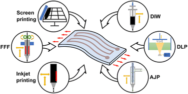
Flexible mechanical sensors (e.g., strain, pressure, and force) fabricated primarily by printing technologies have emerged and evolved promptly in the past several years. 2D and 3D printing approaches enabled rapid prototyping of various flexible mechanical sensors that have demonstrated their unique applications in fields including robotics, human–machine interfaces, and biomedicine. Research efforts have primarily been focused on experimenting with different materials, device configurations, and sensing mechanisms to achieve better sensing performance. While great progress has been made, this field is still in its infancy where most research is exploratory; and even the performance standards and long-term objective/vision of these sensors are not clear. In this review, the state-of-the-art of three types of printed flexible mechanical sensors will be discussed and analyzed in terms of their fabrication methods, types of sensing materials and mechanisms, and challenges for future development.


image file: d2nr04015h-p1.tif

Samuel Smocot

Samuel Smocot is an undergraduate student at McGill University in Montreal, Canada. He will be receiving his B.Eng. degree in Mechanical Engineering (Honours) in 2023. He is currently a student in Prof. Changhong Cao's lab, working on 2D materials and thin films.

image file: d2nr04015h-p2.tif

Zixin Zhang

Zixin Zhang is a graduate student in the M.Sc. program at McGill University under the supervision of Prof. Cao. He received his B.Eng. degree in Mechanical Engineering from McGill University in 2022. He focuses on exploring the manufacturing and reinforcement of nanocomposite materials using 3D printing technologies.

image file: d2nr04015h-p3.tif

Lingzhi Zhang

Lingzhi Zhang received his B.Eng. degree in Mechanical Engineering from McGill University, Montreal, Canada in 2022. He is currently working towards his M.Sc. degree in Mechanical Engineering at McGill University under the supervision of Prof. Changhong Cao. His research focuses on micro/nanomanufacturing, MEMS development, and 2D material characterization.

image file: d2nr04015h-p4.tif

Shu Guo

Shu Guo is an Assistant Professor in the Department of Vehicle and Energy of Yanshan University, China. He received his Ph.D. degree from the Department of Civil Engineering, Johns Hopkins University in 2017. He conducts research in computation mechanics with particular focus on the multi-scale and multi-physics models of composite and piezoelectric materials.

image file: d2nr04015h-p5.tif

Changhong Cao

Changhong Cao is an Assistant Professor in the Department of Mechanical Engineering and the Principal Investigator of McGill Nanofactory at McGill University, Montréal, Canada. He received his Ph.D. degree in Mechanical Engineering from the University of Toronto in 2016 and was a postdoctoral fellow at the Massachusetts Institute of Technology before joining McGill University in 2020. His research expertise is in nanomechanics, printing technologies (2D/3D), micro/nanomanufacturing, MEMS, and low-dimensional materials.


1. Introduction

The development of mechanical sensors (e.g., strain, pressure, and force sensors) can be dated back to the 1950s, when stress-induced changes in the electrical resistance of multi-junction materials (e.g., silicon and germanium) were identified.1 By leveraging the piezoresistive effect, silicon-based strain and force sensors were first invented and applied as important mechanical measurement devices.1–3 These sensors were fabricated mainly by the manual assembly of multiple materials, during which it was difficult to maintain consistency or avoid mismatch when laminating dissimilar materials, such as metal and silicon, under large stress.1,3 Also, the slicing of silicon wafers was not mature enough at the time to produce high-quality and thin silicon wafers.3,4 With the advancement in semiconductor technology, the manufacturing challenges of silicon/bulk material-based mechanical sensors were gradually addressed over time. Their integration into complex electronics boomed and have stayed as the mainstream types of mechanical sensors even today.5

As new technologies emerge (e.g., intelligent robots with human interactions,6–10 advanced biomedical equipment,11–16etc.), conventional bulk materials (i.e., silicon)-based mechanical sensors can no longer satisfy industrial needs, and novel mechanical sensors with advanced functionalities are demanded, including flexible sensors that can undergo large deformations.17–19 For example, mechanical sensors are critical components to build human-like robots where they can be used to provide feedback from mechanical contacts;20 however, the rigidity of bulk materials affects the quality of signal transductions on curved surfaces and limits their application in soft contact scenarios.21–23 By introducing flexibility into mechanical sensors, they can be mounted onto the fingertip, wrist, elbow, and many other complex geometry surfaces of intelligent robots and human interaction interfaces to achieve flexible tactile sensing with high resolution and fast response time.24,25 In addition, making sensors flexible allows electronics to be embedded in unit cells with different orientations, which enables the capturing of multidimensional contact forces.26 The ability to detect normal and shear force entailed the use of flexible mechanical sensors for sophisticated and dexterous manipulation by emulating the mechanical perception in human skin.3,26,27 Moreover, in the biomedical field, mechanical pressure sensors need to be flexible for human interface measurement as it is apparent that rigid sensors do not conform to the soft human tissue and may cause problems to the biological surfaces that they are attached to.17 Flexible mechanical sensors also show exciting potential as a cost-effective alternative to monitor physiological parameters.11,12 Compared to complex and sophisticated equipment that requires experienced personnel and high costs, wearable, miniatured and personalized flexible sensing devices can provide non-invasive diagnosis and health monitoring, encouraging usability in hospital or clinical settings.11,13 Other than robotic and biomedical fields, flexible mechanical sensors are highly applicable in domains where removability and reusability are essential, such as non-destructive testing (NDT) of structures.28,29 For instance, due to the brittle nature of conventional lead zirconate titanate (PZT)-based sensors, they are not reusable in general as the detachment of sensors can easily lead to fracture of the device; also, the requirement of bonding materials to be attached to the testing material makes it difficult to remove without damaging structural surfaces. Flexible strain sensors made with polymeric materials such as polyvinylidene fluoride (PVDF) can be designed to detect defects, such as cracks, impact damage, and delamination by collecting and analyzing the frequency response, natural frequency, and the damping ratio of the structure.29

Conventionally, flexible mechanical sensors are made in cleanrooms through photolithography-based microfabrication processes.30 While microfabrication generally yields high quality devices, it is a time-consuming and expensive process.31,32 Photolithography is great at mass producing a sensor with a mature design ready for commercialization. However, there is an important need for fabrication technologies that can enable rapid prototyping of flexible mechanical sensors since most of their development is still in its infancy.

Fabrication of flexible mechanical sensors by printing technologies have emerged as a versatile, economical, and enabling approach. For instance, various types of mechanical sensors (e.g., force,33–35 pressure,36–40 and strain41–46) can be produced by leveraging many 2D/3D printing techniques including but not limited to screen printing,47–51 inkjet printing,52–56 direct ink writing (DIW),57–59 digital light processing (DLP),60–62 and fused filament fabrication (FFF).63–66 The additive nature of printing technologies also largely reduces the fabrication cost and time;67,68 in addition, fabrication by printing enabled the production of flexible mechanical sensors with excellent performance. Currently, some of the printed flexible mechanical sensors have demonstrated their unique applications in fields such as healthcare, robotics, etc. For example, a silver/rubber-based flexible strain sensor was applied on human joints to recognize motion signals.69 This inkjet-printed strain sensor demonstrated a stable gauge factor (GF) of 8–10, a linear response, and repeatability in performance after cyclic loading; its flexibility also allowed for its conformal fit onto various joints (e.g., wrist, knee, and finger) for accurate movement detection; similarly, a flexible strain sensor fabricated via the FFF can closely adhere to the skin to monitor the bending of the lumbar vertebra of a patient for posture correction purpose;70 additionally, the integration of a screen-printed silver-nanoparticle-based strain sensor into a pneumatic soft actuator on robotic fingers enabled the real-time detection of irregular movement patterns and assessment of finger stiffness or dexterity.71

In addition to strain sensors, printed flexible pressure sensors have also been demonstrated in many applications. For example, an inkjet-printed wearable pressure sensor was used to monitor the bending motions of the wrist and fingers of an operator.72 This carbon nanotube (CNT)/polydimethylsiloxane (PDMS)-based pressure sensor showed great sensitivity on both bare skin and joints and enabled a human–machine-interface to remotely control a tank-like robot with six distinct commands. Also, a DLP-printed hydrogel-based pressure sensor allowed the subtle detection of various forces, which can potentially be applied for prosthetic applications.40 Moreover, an inkjet-printed flexible pressure sensor can be inserted below the cotton fabric of band-aids and other medical dressings to monitor how secure the dressing is attached to a wound to reduce the risk of ischemia.55 Besides strain sensors and pressure sensors, flexible force sensors can also be fabricated via printing technologies and several reports have demonstrated their applications in robotic gripping. For example, a DLP-printed force sensor can be worn as gloves by humans or robots to measure the temperature and contact forces simultaneously.18

In this review, a brief overview of the printing technologies commonly used for the fabrication of flexible mechanical sensors will be reviewed, which will be followed by a discussion of three major types of flexible mechanical sensors individually: strain sensors, pressure sensors and force sensors. This discussion is centered on the performance of the sensors, examining their various sensing materials and sensing mechanisms. Finally, the review will be concluded with our brief outlook on the challenges in the emerging field of printed flexible mechanical sensors.

1.1 Fabrication technologies

As briefed above, several printing technologies have been utilized for the fabrication of flexible mechanical sensors including but not limited to screen printing, FFF 3D printing, inkjet printing, DIW 3D printing (or robocasting), DLP 3D printing, and aerosol jet printing (AJP). While it is not the focus to discuss the details of these printing technologies in this review, a brief overview of their basic working principles and applications in the fabrication of flexible mechanical sensors is summarized as follows.

Screen printing (Fig. 1a) is a conventional printing technique that uses a stencil or mesh to transfer ink onto a substrate.73 The mesh has design patterns where the unnecessary areas are blocked, preventing the ink to be deposited on the substrate.73 Ink is first cast on the screen evenly and a blade is then moved over to push/spread the ink through the openings of the mesh.74,75 Screen printing is not only a scalable process but can also be used on almost any substrate (e.g., textiles, fabrics, papers, metals, plastics, ceramics, glass, or cardboards).73,76FFF (Fig. 1b) is an extrusion-based 3D printing technique where thermoplastic polymer filaments are extruded through a heated nozzle, deposited on a substrate layer-by-layer, and cooled into a 3D structure.77–79 FFF is probably the most adopted 3D printing technology by the general public thanks to its low cost and user-friendliness.80,81Inkjet printing (Fig. 1c) is a non-contact droplet-based printing technique that releases droplets of ink to specific locations on a substrate.82 Inks are released from a cartridge into the printer head, where a thermal actuator or piezoelectric transducer generates an impulse that pushes a droplet through the nozzle.82 It should be noted that for the fabrication of flexible mechanical sensors, 2D inkjet printing is generally used, which is different from inkjet 3D printing (material jetting) where jetted inks are cured and built layer-by-layer into a 3D structure. The advantage of inkjet printing is its high pattern resolution and precision.83DIW (Fig. 1d) is another extrusion-based printing technique that dispenses shear-thinning ink through a syringe nozzle driven by compressed air and deposits materials in a layer-by-layer manner to build up 3D structures.84,85 The advantages of DIW include its ability to print at room temperature and ability to also allow multi-material printing.57,58,86DLP (Fig. 1e) is a type of stereolithography (SLA) 3D printing technology that uses ultraviolet (UV) light to solidify an entire layer profile across a photocurable resin and build up 3D structures layer-by-layer.60 DLP has a crucial component called digital micromirror device (DMD) consisting of an array of reflective micromirrors.60,61 These micromirrors enable precise projection patterning by turning “on” and “off” independently throughout the process.61 DLP in general is a high-resolution (microscale) and fast printing approach (compared to SLA).62AJP (Fig. 1f), also known as maskless mesoscale material deposition (M3D™), is a non-contact, droplet-based, direct-writing printing technique.87–89 AJP uses aerodynamic focusing to precisely jet out aerosol, a suspension of small ink droplets in a gas, onto a planar or curved substrate and deposits a layer of material.88–91 The advantages of AJP are fast printing speed, fine resolution, and a wide scope of material selection.91,92 Compared to the other commonly used FFF technology, which has a typical limiting speed of 80 mm s−1, AJP can print at 200 mm s−1 with a dynamic accuracy of ±6 μm (ref. 92 and 93) while maintaining a resolution of 10 μm.90,91 Besides, AJP can handle a variety of materials ranging from natural semiconductors and carbon nanomaterials to ceramics and composites with viscosities between 1 and 2500 cP.91,92


image file: d2nr04015h-f1.tif
Fig. 1 Schematics of (a) screen printing; (b) FFF 3D printing; (c) inkjet printing; (d) DIW 3D printing; (e) DLP 3D printing; (f) aerosol jet printing, and typical components of flexible mechanical sensors that each technology is used for.

Generally, a flexible mechanical sensor consists of several primary components including a sensor body (substrate), a sensing element, and a circuit.94 While an individual flexible mechanical sensor has its unique structure and may not necessarily have all the aforementioned components or may have other features, it typically consists of a compliant material that can deform to a certain extent while maintaining its performance.94–96 Printing technologies have been adopted to fabricate most of these components,65,70,97,98 although depending on the type of sensor, some printing approaches are preferrable over others (Fig. 1).

Flexible strain sensors normally consist of an insulating flexible substrate and a conductive thin film circuit.99 The bottom side of the flexible substrate is glued to the surface of the target object,100 and the circuit measures the deformation using changes in electrical signals.101 To fabricate flexible strain sensors, FFF has been adopted as one of the most prevalent printing methods because of its simplicity and low cost (Table S1).63,65,70,97,98,102,103 When FFF is adopted for the fabrication of flexible strain sensors, the entire sensor, including the sensing element and the substrate, is normally printed by the extrusion of custom-made filaments, usually conductive nanocomposites63,65,98 (e.g., graphene nanoplatelets (GNP)/CNTs/thermoplastic polyurethane (TPU)), into desired configurations. FFF is popular because it enables printing of the substrate and the sensing element altogether. The printed parts can be used directly after printing without much post-processing. In addition, the digitally controlled nozzle of FFF printing can precisely deposit a material at the desired location with a fine thickness,63,65,97,104 meeting the need of printing thin foil grid patterns in many flexible strain sensors. Besides FFF, inkjet printing is also a prevalent technique for producing flexible strain sensors. It is generally used to print the sensor circuit (e.g., microchannels and conductive paths) on flexible substrates instead of printing the entire sensor itself. Inkjet printing features accurate position control,53,105–107 which makes it suitable for precise deposition of the circuit pattern and enables a complicated circuit design. It is also a time-consuming process because of its small volume printing feature which increases the resolution.

Flexible pressure sensors basically have three working mechanisms: piezoresistive, capacitive, and piezoelectric.108 When a pressure is applied, the capacitive sensor changes its distance between the two electrodes, thus leading to a change in capacitance.109 The piezoelectric sensor generates an electric potential across the piezoelectric element when pressure is applied,55,110 while the piezoresistive sensor displays a change in electric resistance that depends on the distance between the conductive particles.55,111 Flexible pressure sensors55,112–114 have been preferentially fabricated by screen printing that allows printing of a variety of material types112–115 with various rheological properties, in contrast to DIW or inkjet printing. Silver-based (nanowires112 and nanoparticles51) and carbon-based (e.g., CNTs)115,116 inks are two common types of inks used to fabricate electrodes on a flexible substrate. For example, Guo et al. used screen printing to fabricate electrode arrays on a polyethylene terephthalate (PET) substrate with nano-silver ink.113 Emon et al. screen printed multi-walled carbon nanotubes (MWCNTs)/polymer paste on a substrate to make stretchable electrodes.117 The printed electrodes often have a simple geometry and do not require high printing resolution. In addition, compared to other printing techniques which usually deposit a line of material in each printing cycle, screen printing can deposit a layer at a time and reduce the manufacturing time. Yang et al. claimed that hybrid screen printing and the electrospinning process with high throughput have numerous advantages including high efficiency, trouble-free operation, minimal waste, low manufacturing cost, and large-scale production ability.118 DIW is another favored method to fabricate flexible pressure sensors. As a versatile printing technique, DIW can work with a wide variety of materials from MWCNTs/PDMS ink119 to silver ink.120 Various components can be printed with this technique, including the dielectric layer,119 electrodes,120 substrate,57 and the sensing element.121 Fekiri et al. were able to fabricate a flexible pressure sensor with high sensitivity (6.3 Ω kPa−1) and a wide range of measured pressures (up to 1132 kPa) using MWCNTs dispersed in a PDMS prepolymer.119 However, the drawback of DIW is that it requires shear-thinning ink to be engineered and the process can be time-consuming.

Flexible force sensors measure forces using a capacitive approach or piezoresistive approach in general. Similarly to the aforementioned flexible pressure sensor, the capacitive approach operates on changes in capacitance and the piezoresistive approach operates on changes in resistance. FFF is also a prevalent technology used to fabricate flexible force sensors, in most cases the entire sensor, via the extrusion of conductive polymers, such as TPU filaments. Another favored printing method for flexible force sensors is screen printing. With this method, electrodes are the most commonly printed components. As mentioned earlier, screen printing has the advantage of fast printing speed but cannot print complicated designs like the other digitally controlled techniques. Besides, the cost-effectiveness of screen printing makes the use of large area electronic or tactile skin in robotics possible.122

While AJP35,45,67,123 and DLP38,40,42,43,124,125 have been applied for the fabrication of flexible mechanical sensors, they are less common due to various reasons. For example, although AJP is a newly developed printing technique with high resolution91 and fast printing speed,90 the cost of AJP is much higher in contrast to other techniques; while DLP can fabricate sophisticated 3D geometries with high resolution and rapid speed, the requirement of a photocurable resin limits the material selection.

2. Mechanical sensors by type

2.1 Printed flexible strain sensors

Flexible strain sensors found their applications in many fields as mentioned above and a variety of sensing materials were explored via printing technologies to achieve high performance, including silver, carbon black (CB), CNTs, graphene, and other highly conductive materials. However, printed flexible strain sensors are still an emerging field, as the majority of works published in this domain are from the past several years. As such, the clear cut “best” material or best approach to printing a flexible strain sensor has not yet been determined. In this section, printed flexible strain sensors will be discussed based on the type of sensing material; and a comparison in terms of their sensing performance is summarized in Fig. 2. The most interesting performance metrics of flexible strain sensors are their GFs, strain sensing ranges and cyclic ability. Since many of the studies in the literature did not report the cyclic ability of their sensors or did not perform cyclic tests until failure, only GFs and strain sensing ranges are compared here.
image file: d2nr04015h-f2.tif
Fig. 2 (a) GF as a function of the tested strain range of recently reported printed flexible strain sensors grouped by the sensing material. Some works did not report the GF in the entire sensing range (e.g., not from 0%) because the GF was not constant in that range. GF is illustrated as a scatter point in instances where the GF was only reported at one point. (b) Magnified view of the boxed area in (a). * GF values were read directly from the plot of ΔR/R0vs. strain curves; sensing material also includes AgNPs; †† sensing material also includes GNPs.

Silver (Ag), CNTs, graphene, and CB are common active sensing materials in printed flexible strain sensors, whose conductivities are summarized in Table 1. As shown in Fig. 2, Ag-based sensors provide good sensing performance (GFs of mostly 10 and above), especially if used in tandem with an appropriate structure.43,69,123,126–128 The GF is defined by the change in electrical resistance under stretching over strain: GF = (ΔR/R0)/ε, where R0 is the initial electrical resistance, ΔR is the change in resistance, and ε is the strain.128 CNT-based sensors have a large sensing range and high GFs; the sensing range of graphene-based sensors is larger than most other sensors as well, and CB-based sensors have an average performance when it comes to the sensing range and GF. Factors determining the GF and sensing range include the conductivity of the active sensing materials (fillers), the stretchability of the elastomer matrices, the capability of conductive composites to maintain electrical properties under deformation, and the configuration of the sensor.

Table 1 Conductivities of pure characteristic materials used in printed flexible strain sensors
Material Conductivity [S m−1] Ref.
Ag (printed ink) 3.1 × 10⁶ 129
Single walled CNTs (thin film) 2.5–4 × 10⁴ 130
MWCNTs (paper) 5 × 10³ 131
Graphene (paper) 1.4 × 10³ 131
Carbon black (paper) 9 × 101 131


2.1.1 Silver-based. As shown in Fig. 2, a large proportion of printed flexible strain sensors with high GFs is silver-based,43,69,123,126–128 largely due to silver's excellent conductivity.69 The majority of them are fabricated by printing a conductive silver ink,43,127 that may contain either silver nanowires (AgNWs)126 or silver nanoparticles (AgNPs),123 on a flat flexible substrate. The concentrations of the Ag-based inks were tuned in these studies such that the interactions between the AgNPs or AgNWs during deformation are in the right range to cause detectable resistance changes. Too low of a concentration will result in disconnections in the conductive path, while too high will lead to a low GF as the change in the interactions between the AgNPs or AgNWs will be too small.126 The highest GF reached among the flat silver-based sensors43,123,126,127 is in the 4.32–5% strain range obtained by Gai et al.127 Their sensor was fabricated by inkjet printing silver ink onto a polyurethane acrylate (PUA) substrate. When a tensile strain is applied, the silver particles will be pulled apart, which leads to a resistance increase. Fig. 5e illustrates this destruction mechanism also used in a CB/AgNP bending-strain sensor,132 which will be further discussed in the Bending-strain sensors section below.

Apart from the concentration of AgNWs or AgNPs in the conductive ink, optimal design of the sensor's structure is another way to enhance the sensing performance. Han et al. developed a sensor (Fig. 3a) that has a sandwich structure prepared by FFF 3D printing TPU fibrous textiles as the upper and lower layers, with a AgNP pulp solution deposited in-between.128 As shown in Fig. 3b, the lamination orientation was designed in such a way that the applied force to the sensor was exclusively in the diagonal direction. The angle (θ) between the upper and lower textiles will decrease upon stretching, and the elongation of TPU fibers will lead to an increase in resistance caused by the separation of AgNPs in the conductive network. This deformation of TPU fibers leads to the compression of the sandwiched AgNPs in the grooves between the TPU fibers where the AgNPs become denser and act as a warehouse of AgNPs for the conductive network. This effect cannot fully compensate for the disconnection of AgNPs at higher strains, meaning the rate of increase in the resistance of the sensor was larger in the higher strain ranges compared to that in the low strain ranges, which contributes to the GFs of 2374, 4180, 11[thin space (1/6-em)]477, and 38[thin space (1/6-em)]220 for the strain ranges of 0–60, 60–90, 90–120, and 120–138%, respectively. Besides Ag, other metal-based sensing materials were used in similar fashions in flexible printed strain sensors as well but not quite extensively and their performances were not as good as the Ag-based ones; for example, Bhuiyan et al.133 used nickel lines printed in various patterns on polyimide and polyethylene substrates and Ahmadi et al.46 printed indium tin oxide (ITO) patterns onto PET substrates.


image file: d2nr04015h-f3.tif
Fig. 3 Representative printed flexible strain sensors and their sensing mechanism. (a) Architecture of a printed TPU/Ag composite-based flexible strain sensor; (b) sensing mechanism illustration of (a).128 This figure has been reproduced from ref. 128 with permission from John Wiley and Sons, copyright 2021; (c) schematic illustration of the coaxial printing process and the optical image of ink extrusion.134 This figure has been reproduced from ref. 134 published under the Creative Commons license (no copyright); (d) sensing mechanism of (i) a single-layer sensor without cracks, (ii) a single-layer sensor with cracks, and (iii) a double-layer sensor with cracks.49 This figure has been reproduced from ref. 49 with permission from Elsevier, copyright 2022.
2.1.2 CNT-based. It can be seen from Fig. 2 that the reported maximum sensible strain of some CNT-based sensors49,63,65,97,134 can reach up to 350%.65 Even though the strain ranges of some of these sensors are not reported/completely plotted in Fig. 2 due to the lack of experimental data or the non-linearity in the GF in certain strain ranges, a few of these CNT-based sensors are also among the sensors with the highest GFs as shown in Fig. 2. These characteristics are largely due to (i) the high conductivity130,131 and superior mechanical properties of CNTs,135 (ii) the great elasticity of the polymer matrices used as the building block materials, and (iii) great interactions between the CNT networks in the polymer matrices when under large deformation. For example, Xiang et al. FFF-printed a flexible strain sensor made of CNTs and GNP in a TPU matrix that was able to sense strains up to 250% without failure.63 The sensor's assembly consists of two CNTs/GNPs/TPU fiber layers; all fibers are parallel to each other within each layer, and the two layers are stacked in such a way that the fibers in the top layer are perpendicular to the fibers in the bottom layer. It has a similar structure to the TPU fibers in Fig. 3a. While its GF is not constant, it increases along with the applied strain and can reach a maximum of 136[thin space (1/6-em)]327 at 250%. Additionally, via DIW, Tang et al. printed a flexible strain sensor in a core–shell structure (Fig. 3c) with the shell made of a silicon nanoparticle (SiNP)-based silicone elastomer and the core made of Ecoflex (silicone rubber)/CNT powders.134 The reported GFs of this sensor are 1.4 and 2.5 × 10⁶ for the respective strain ranges 0–25% and 90–150%. The sensing mechanism of this sensor is not discussed by the authors, but the fiber-like shape of this sensor was chosen for its flexibility, wearability (easy integration into fabrics), and light weight.

In addition, the introduction of defects can be leveraged to engineer the performance of CNT-based flexible strain sensors. For example, to increase the dispersibility and binding of CNTs in the polymer, waterborne polyurethane (WPU) and WPU-OH were used to functionalize the CNTs to make a CNT/polymer-based ink suitable for screen printing.49 Three different sensors were screen-printed: a single-layer sensor without cracks, a single-layer sensor with cracks, and a double-layer sensor with cracks (Fig. 3d). The single-layer sensor without cracks turned out to have the lowest sensitivity among the three; the single-layer sensor with cracks had an ultra-high GF but a very small sensing range; the double-layer sensor with cracks demonstrated the best performance where it could detect strain up to 120% and had a GF of 2000 at 18% strain. The reason is that, as shown in Fig. 3d(iii), for the double-layer sensor, the crack propagation rapidly increases the resistance of the sensor. The high strain range reached is due to the double layer being able to maintain the conductivity of the sensor at high strains; the current is driven to move in an S-shape during stretching which maintains the conductive path. When the sensor is unstretched, the current only flows through the upper layer because it has a lower resistivity than the lower layer. Upon stretching, the current follows a cycle of encountering a crack and flowing to the lower layer before flowing back up to the upper layer.

2.1.3 Graphene-based. All graphene-based flexible strain sensors identified in the literature have a relatively large sensing range,124,136–138 as shown in Fig. 2. Similarly to the aforementioned types, the mechanical configuration of a sensor and the mechanical/electrical properties of the sensing materials are key determining factors of their sensing performance. For example, Qian et al. DLP-printed a reduced graphene oxide (rGO)/elastomer resin (ER) composite into a flexible strain sensor.124 Possibly due to the good tensile properties of the ER made of acrylated aliphatic epoxy (EAA) and aliphatic urethane diacrylate (AUD) and a great distribution and interactions of rGO, the sensors can sense strain up to 60%. While a single printed line of rGO/ER (the unit sensing element) exhibited a GF of 6.723 for 0–40% strain, the GFs of the printed electrodes were less than that of the printed line and varied based on the angle of the sensor's rhombic structure (Fig. 4a). The rhombic structure with tan(θ) = 0.5, where θ is the angle between the vertical axis and the side wall of the rhombic structure, had the highest GF among the three sensors: 3.374 in the 10–40% strain range while only 1.031 for 0–10% strain; whereas the rhombic structure with tan(θ) = 1.5 was the only one with a constant GF of 2.344 over its entire strain range of 0–60%. The angle θ of the rhombic structure leads to different stress distributions (Fig. 4a), which in turn leads to different resistance changes among the different rhombic structures, explaining the differing GFs.
image file: d2nr04015h-f4.tif
Fig. 4 Representative printed flexible strain sensors and their sensing mechanism. (a) Tensile process and the stress simulation results of rGO/ER composite rhombic structures at various tan(θ).124 This figure has been reproduced from ref. 124 with permission from John Wiley and Sons, copyright 2021; (b) optical images of the 3D printed graphene/PDMS composites with (i) the grid structure, (ii) the triangular porous structure, and (iii) the hexagonal porous structure.136 This figure has been reproduced from ref. 136 with permission from IOP Publishing, copyright 2019; (c) schematic diagram illustrating the sensing mechanism of the rGO–Pd nanocomposite: (i) contact area mechanism, (ii) charge tunnelling mechanism.137 This figure has been reproduced from ref. 137 with permission from IOP Publishing, copyright 2021; (d) schematic illustration of graphene, AgNPs and the graphene/AgNP hybrid conductive film (i) before stretching and (ii) after stretching.138 This figure has been reproduced from ref. 138 with permission from Kluwer Academic Publishers (Boston), copyright 2020.

Wang et al. also leveraged structural differences to create graphene/PDMS composites with tunable GFs.136 The porous graphene/PDMS composites were printed via DIW into three porous structures (Fig. 4b): grid, triangular, and hexagonal porous structures. The GF of the printed sensors was tuned by designing different porous structures such that their strain responses to deformation are different, which further led to changes in the resistance. Over the 0–20% strain range, the hexagonal porous structure had the largest GF (∼67), while the grid structure had the lowest (∼6).

Nuthalapati et al. fabricated a rGO/palladium nanoparticle (PdNP)-based sensor by screen printing rGO–Pd ink sandwiched between two PDMS layers.137 Palladium (Pd) was used for its higher strain sensitivity compared to other metals. The sensing mechanism is explained based on the contact area and tunnelling mechanisms (Fig. 4c). Under tensile strain, the overlapping area between rGO sheets decreases, which leads to an increase in resistance (Fig. 4c(i)). The tunnelling mechanism refers to the increase in tunnelling distance, i.e., the distance between adjacent PdNPs or rGO sheets and other PdNPs or rGO sheets (Fig. 4c(ii)). Experimental data showed that the larger change in resistance was due to the tunnelling mechanism rather than the contact area mechanism. The sensor's GF ranged from 14 at 0.1% strain to 1523 at 45% strain.

Htwe et al.'s strain sensor was made by inkjet printing graphene/AgNP ink onto a polyvinyl alcohol (PVA) substrate.138 Inks with different concentrations of graphene ranging from 0.1 wt% to 0.7 wt% were prepared to investigate their effects on properties, including electrical conductivity. It was found that the conductivity of the ink increased with the increasing concentration of graphene, until reaching the percolation threshold of 0.5 wt%. The graphene/AgNP sensor's GF was 149 over the 0–20% strain range, which is better than both their graphene-only sensor with a GF of 97 and their AgNP-only sensor with a GF of 76. These sensors’ lower GFs are explained by the fact that AgNPs or graphene flakes on their own cannot maintain the conductive network during stretching as well as the graphene/AgNP hybrid sensors (Fig. 4d). In the graphene/AgNP composite, the graphene flakes tend to align, keep the distance between the graphene flakes and AgNPs close and maintain the conductive path.

2.1.4 Carbon-black based. Besides the sensor structure and the concentration of the conductive sensing material, the sensitivity of nanocomposite-based sensors is greatly affected by the size and shape of the nanostructures (e.g., the high aspect ratio of CNTs is prone to entanglement).70 Carbon-black particles (CBPs) in the form of flakes/spheres are relatively easier to be dispersed in a polymer matrix,70 much cheaper compared to other carbon nanomaterials,132 and have great conductivity as well.139 Li et al. fabricated CB-based flexible strain sensors where a TPU/CBP composite filament was extruded via FFF onto a TPU substrate.70 Sensors with various periodic structures (Fig. 5a) were printed to investigate the effect of structure on the sensor's performance. The configuration with the largest linear range (i.e., where the GF was constant) was the rectangular zigzag (RZ) structural sensor that exhibited a constant GF of ∼1.6 over the strain range of 0–15%. The different periodic structures exhibited different geometric deformations, which led to the difference in GFs. The periodic configuration determines the levels of elongation and shrinkage along the tensile and vertical directions. The RZ structural deformation was steadier than the S-shaped zigzag (SZ) and triangular zigzag (TZ) configurations, leading to its larger linear sensing range. As seen in Fig. 5b, upon tensile strain, the remodeling or even destruction of the conductive network created by the filler CBPs causes the sensor's resistance to increase. When tension was released, the conductive network was reconstructed, and the resistance returned to its original value. Besides, Kouchakzadeh et al. used a dual extruder FFF to print a sensor constituted of a TPU matrix and conductive channels made of acrylonitrile butadiene styrene (ABS) with CB elements (Fig. 5c).44 Their sensor's response mechanism is based on the increase in electrical resistance when the sensor is stretched; the instantaneous resistance is given by R = ρL/A where ρ is the material's specific resistance, L is the conductive channels’ length, and A is their cross-sectional area. Upon tension, L increases which in turn increases the resistance R. Their sensor's GF ranged from ∼2.25 to 3 for strain between 0 and 22%.
image file: d2nr04015h-f5.tif
Fig. 5 Representative printed flexible strain sensors and their sensing mechanism. (a) Sensors with a CBP/TPU composite and a pure TPU-film substrate. The various periodic configurations shown are (i) SZ, (ii) TZ, and (iii) RZ;70 (b) sensing mechanism of sensors in (a). S0 denotes the minimum spacing between two CBPs for a conductive path to be built.70 These figures have been reproduced from ref. 70 with permission from Elsevier, copyright 2022; (c) printed flexible ABS/TPU strain sensor before and after deformation.44 This figure has been reproduced from ref. 44 with permission from Elsevier, copyright 2021; (d) screen-printed CB/AgNP-based bending strain sensor and (e) its sensing mechanism.132 These figures have been reproduced from ref. 132 published under the Creative Commons license (no copyright).

While both CB-based sensors discussed here are not impressive in terms of GF compared to the other material-based ones (Fig. 2), their performance being good enough to meet usage requirements70 and their cost effectiveness demonstrate that CB is a sound material choice for flexible printed strain sensors.

2.1.5 Bending-strain sensors. Aside from the previously discussed strain sensors, there are also printed flexible strain sensors specialized for sensing bending strain only, i.e., the applied strain resulting from the bending of the sensor rather than stretching/compressing. It is usually defined by ε = h/(2r) where h is the thickness of the sensor and r is the radius of curvature (or bending radius),132 but it may also be defined as strain given by ε = Δl0/l0, where Δl is the length change of the sensing layer and l0 is the initial length.140 The bending strain is much smaller (order of 1%) compared to the strain induced by in-plane stretching, which normally translates to much higher GFs than tensile/compressive strain sensors.

The sensing materials of these sensors include laser-induced graphene,141 CB composites,132,140 CNTs,142 and AgNWs.143 For example, Qi et al. screen-printed a AgNP/CB nanocomposite onto a PET substrate to fabricate a bending strain sensor (Fig. 5d) that achieved a very high GF of 444.5 over 0.6–1.4% applied strain.132 The high GF reached was attributed to the large variation in the junction resistance of the printed patterns under tension. The sensor's active layer contains a percolating lattice of overlapping nanomaterials which enables the electrons to pass through. Under bending, there is a reduction of overlapping areas or even a separation of electrical connections, illustrated in Fig. 5e, which increases the junction resistance in the sensor.

Xiao et al. constructed a bending-strain sensor with a laminate structure of polyvinyl chloride (PVC)/CB/silver.140 The sensing mechanism of this sensor also relies on the formation of cracks to alter the PVC/CB film conductive path. It took 5500 bending cycles for the sensor's performance to stabilize i.e., the initial value of sensor resistance being equal to the final value. As the number of bending cycles increased, the amount and size of the cracks increased as well, until they eventually reached their maximum length and width, leading to the stabilization of the sensor's performance. The GF of this sensor was 741 for 0–0.14% tensile strain, and −1563, −47 for the respective compressive strain ranges 0–0.04% and 0.04–0.14%.

2.2 Printed flexible pressure sensors

Similarly to printed flexible strain sensors, printed flexible pressure sensors are primarily made of silver, CNTs, graphene-based composites or by printing of these highly conductive materials on a flexible polymeric substrate. The main criterion of interest in flexible pressure sensors is their sensitivity, generally defined by S = δ(ΔE/E0)/δP, where ΔE is the electrical signal change (e.g., current, capacitance), E0 is the initial electrical signal (capacitance for capacitive sensors and current for piezoresistive sensors), and P is the applied pressure.39 Other criteria of interest include their detection range, lower detection limit and cyclic ability. As was the case for the strain sensors discussed above, the cyclic ability of these sensors was not reported consistently across all works, making it difficult to compare.

Two major sensing mechanisms were identified for pressure sensors: capacitive and piezoresistive. Capacitive sensors have a sandwich structure composed of electrodes on the outside and a dielectric layer in the middle. Under applied pressure, the distance between the electrodes changes, which in turn yields a change in the capacitance.144 The capacitance can also be altered due to the changes in the permittivity occurring in the dielectric layer.116 On the other hand, piezoresistive sensors vary much more in structure since their sensing mechanism is based on the contact area change. The contact resistance is more dominant compared to the inherent resistance of the sensor's materials,39 which means the total resistance of the sensor can be controlled by varying the contact area inside the sensor and therefore varying the resistance. As the electrical resistance changes under pressure, the current flow also changes, enabling pressure detection.

From Fig. 6, some interesting observations can be made (note: the sensing material of the capacitive sensors refers to the dielectric layer material; while that of piezoresistive sensors refers to the conductive film/filler material used). Among the capacitive pressure sensors,51,55,112–114,116,144–146 it is interesting to find that the sensitivities of the sensors are generally lower at high pressures compared to the sensitivities for low pressure sensing because once the sensor's dielectric layer has already been compressed, compressing it even further takes a lot more pressure116 which would decrease the sensitivity according to the given sensitivity equation above. Also, silver-based sensors in general have higher sensitivities compared to CNT-based and polymer-based sensors, but the latter are able to maintain their sensitivity (albeit lower than silver-based sensor's sensitivity) for larger pressure ranges. It should be noted that no matter what sensing material is chosen, using a dielectric with high permittivity is a very important factor for achieving high sensitivity with a capacitive pressure sensor.112,113,116 For piezoresistive pressure sensors, it is clear from Fig. 6 that CNT-based ones are most popular followed by graphene-based and polymer-based sensors. In addition, some printed flexible piezoresistive pressure sensors can achieve higher sensitivities than their capacitive counterparts in comparable pressure ranges. For example, Zhang et al.'s graphene-based sensor,147 Xia et al.'s gold nanoparticle (AuNP)-based sensor,148 and Ma et al.'s CNT-based sensor50 all had higher sensitivities than the best-performing silver-based capacitive sensor (Wang et al.116). From Fig. 6, there is no clear best choice for sensing materials used in piezoresistive sensors, since both the sensitivity and sensing ranges are scattered for all materials shown. Using graphene-based or CNT-based sensors is a common approach because at least an average sensitivity can be achieved in many cases, which can be much improved if paired with an appropriate design of the sensor's microstructure. This microstructure is key to enabling a large variation in the contact area under pressure, which will cause a large change in the resistance. In the following section, the two major types of printed flexible pressure sensors will be discussed in more detail categorized by active sensing materials.


image file: d2nr04015h-f6.tif
Fig. 6 Sensitivity as a function of the pressure range of recently reported printed flexible pressure sensors grouped by the sensing material and sensor type (capacitive and piezoresistive). * These works did not report a lower detection limit for their sensor; therefore, a value of 100 Pa was assumed to use a logarithmic scale on the x-axis.
2.2.1 Printed flexible capacitive pressure sensors.
2.2.1.1 Silver-based. Among the capacitive silver-based pressure sensors, AgNP-based conductive ink has been used to print the electrodes of sensors,112 and AgNW composites have been printed into dielectric layers.112,116 Wang et al.'s sensor achieved the highest sensitivity of all capacitive pressure sensors, as shown in Fig. 6.116 An AgNW composite was spin cast as a dielectric for their flexible capacitive pressure sensor. The dielectric layer consisted of TPU elastomer rubber with AgNWs fabricated via electrospinning. These membranes called TPU electrospinning nanofiber membranes (ENMs) had different amounts of AgNWs (1.0 mL–5.0 mL) added to them to examine the effect of the AgNW concentration on the AgNW/TPU composite membrane. The sensor was assembled using a TPU ENM supporting layer with printed CNT ink as electrode layers and the AgNW/TPU ENM dielectric was placed in the middle of the CNT electrode layers. The sensitivity of the sensors increased as the AgNW doping amount increased and decreased as the pressure increased. The addition of AgNWs increased the permittivity of the AgNW/TPU composite dielectric, which explains why the sensor with 4.0 mL of AgNW doping was the one that had the highest sensitivity.

Mo et al. also used a AgNW composite as a dielectric for their flexible capacitive pressure sensor,112 which also achieved a sensitivity higher than the majority of other capacitive sensors (2.1 kPa−1 for 0–0.25 kPa). The dielectric layer was composed of 1 wt% thermal expansion microcapsules (TEMs) (0.5 wt% AgNWs in PDMS),149 and was fabricated by screen printing onto PET. Afterwards, the printed dielectric layer was peeled off and packaged between two AgNP screen printed electrodes onto PET substrates. A sensor without AgNWs was also fabricated to examine the effect of AgNWs on the sensitivity of the sensor. The addition of AgNWs increased the permittivity of the dielectric layer, which in turn increased the sensitivity of the sensor in low pressure ranges; the sensitivity of the AgNW/TEM/PDMS dielectric based sensor was 2.1 kPa−1 for pressures under 250 Pa, which was 2.4 times higher than that of the TEM/PDMS dielectric based sensor. The sensor's sensitivity decreased in higher pressure ranges as shown in Fig. 6 and its detection limit was 1.3 Pa with a loading response time of 50 ms under 100 kPa.


2.2.1.2 Polymer-based. Flexible pressure sensors using polymers as dielectrics and assembled by printing electrodes on top have also been demonstrated.51,55,114,145,146 Maddipatla et al. used PDMS as the dielectric layer sandwiched between screen printed CNT-based electrodes (Fig. 7a).144 The sensitivity obtained was unfortunately very low though, 0.000212 kPa−1 for 0–350 kPa, among the lowest in Fig. 6. Masihi et al.'s PDMS-based sensor was able to sense at higher pressures (the second largest pressure of all capacitive sensors shown in Fig. 6, 900 kPa); however, it also has low sensitivity and a long response time (∼0.8 s).114 Its porous PDMS dielectric layer was prepared using sodium hydrogen bicarbonate (NaHCO3) and nitric acid (HNO3) to control the pore size and its distribution without the release of toxic gases. To assemble the sensor, the dielectric layer was sandwiched between fabric-based electrodes with Ag ink screen printed on them. Unfortunately, a schematic of the working mechanism of their sensor was not included in their paper. In contrast, Ding et al. were able to obtain a higher sensitivity (1 kPa−1 below 0.4 kPa) that is comparable to the best-performing capacitive sensors shown in Fig. 6 using silica gel as the dielectric and through microstructure design.146 Silver electrode layers were inkjet printed onto PET substrates and the elastic silica gel microstructures were printed via DIW on the bottom silver electrode. The cross-section of the dielectric layer's microstructure is shaped as a microdome (Fig. 7b) to increase the capacitance under pressure and thus increase the sensitivity. As pressure is applied to the sensor, the curved surface of the microdome shaped lines is pressed flat against the electrode layers leading to an increase in the capacitance. However, higher pressures will not deform the dielectric microstructure as easily since it will already be squeezed flat by the high pressure, which results in much lower sensitivity for higher pressures (0.0006 kPa−1 for 50–200 kPa).
image file: d2nr04015h-f7.tif
Fig. 7 Representative printed flexible capacitive pressure sensors. (a) Schematic of a polymer-based capacitive pressure sensor with CNT-based electrodes and its layer alignment.144 This figure has been reproduced from ref. 144 with permission from IEEE, copyright 2017; (b) schematic of another polymer-based capacitive pressure sensor using elastic silica gel microstructures as a dielectric layer on silver electrodes.146 This figure has been reproduced from ref. 146 with permission from IEEE, copyright 2021.

2.2.1.3 CNT-based. Guo et al. developed a flexible pressure sensor using a CNT/PDMS composite as the dielectric layer sandwiched between two printed Ag-based electrodes,113 which achieved the second highest sensitivity among the capacitive sensors shown in Fig. 6. The aspect ratio and mass fraction of the CNT fillers are key factors determining the relative permittivity of the CNT/PDMS composite dielectric, hence the sensitivity of the sensor. Their work explored composites with CNTs of different aspect ratios and wt%. It turned out that composites containing CNTs with aspect ratios of 500–3000 and a mass fraction of 6 wt% have a permittivity 207 times greater than that of pure PDMS. As the mass fraction of CNTs increased, the composites with CNTs of larger aspect ratios experienced faster increases in relative permittivity compared to the ones with lower aspect ratio CNTs. Once again, the sensitivity of the sensor increased as the permittivity of the dielectric increased, which is in agreement with Wang et al.'s116 and Mo et al.'s112 works discussed above.
2.2.2 Printed flexible piezoresistive pressure sensors.
2.2.2.1 CNT-based. Fig. 6 shows that CNT-based sensing materials are commonly used in printed flexible piezoresistive pressure sensors.38,39,50,150 Yin et al.'s DLP printed sensor demonstrated the best linearity among all the piezoresistive sensors plotted in Fig. 6, while also maintaining a decent sensitivity.38 Its lattice structure pressure sensor (shown in Fig. 8a) exhibits a sensitivity of 1.02 kPa−1 for a very wide pressure range (0.7 Pa–160 kPa). The active layer of this sensor is a DLP-printed TPU lattice, coated with CNTs and placed onto a conductive fabric electrode. When pressure is applied, the active layer is squeezed against the electrode, which increases the contact area and further leads to an increase in conductive pathways (i.e., conductivity). Also, when the active layer's lattice structure is under pressure (shown in Fig. 8b), it enhances the interactions between the adjacent beams, which also increase the conductivity of the lattice. This sensor showed excellent cyclic ability as well (i.e., not exhibiting any electrical signal degradation for 60[thin space (1/6-em)]000 loading cycles).
image file: d2nr04015h-f8.tif
Fig. 8 Representative printed flexible piezoresistive pressure sensors and their sensing mechanism. (a) Exploded view of the pressure sensor and (b) deformation of the lattice structure under pressure.38 These figures have been reproduced from ref. 38 with permission from American Chemical Society, copyright 2021; (c and d) sensing mechanism of an occluded PDMS/CNS pressure sensor.39 These figures have been reproduced from ref. 39 with permission from the Royal Society of Chemistry, copyright 2020; (e) assembly of an rGO-coated PDMS based pressure sensor; (f) cross-sectional SEM images of PDMS; (g) contact area change under varied pressure.147 These figures have been reproduced from ref. 147 with permission from John Wiley and Sons, copyright 2019; (h) schematic diagram of the biological microstructure of human skin and the sensor's sensing layer with a skin-inspired structure: an ultrathin-walled cellular graphene layer (top) and a thick-walled cellular graphene layer (bottom).58 This figure has been reproduced from ref. 58 with permission from John Wiley and Sons, copyright 2022; (i) bimodal PEDOT:PSS pressure sensor with a temperature sensing layer on top and a pressure sensing layer on bottom.56 This figure has been reproduced from ref. 56 with permission from Elsevier, copyright 2017.

Li et al. developed a similar sensor based on a PDMS/carbon nanostructure (CNS) composite film fabricated by spray coating CNS onto a PVDF template which was then peeled off and attached onto PDMS via thermal curing.39 It demonstrated sensitivity close to the above sensor.38 Two of these microstructured PDMS/CNS films were placed face-to-face to form a flexible pressure sensor. Three different sensors with different sized PVDF molds were fabricated to study the effect of template mesh size on the sensitivity of the sensor. The best-performing sensor exhibited a sensitivity of 1.214 kPa−1 for pressures under 100 Pa, which is in the top half of piezoresistive sensors shown in Fig. 6. As is the case with most piezoresistive pressure sensors, the sensing mechanism of this sensor also relies on the contact area change, as illustrated in Fig. 8c. As pressure is applied, the microstructure of the occluded pressure sensor experiences variations in contact points and contact areas, which leads to a variation in electrical conduction (Fig. 8d). The geometrical dimension of the microstructure also contributes greatly to the high sensitivity since the height of the microstructure must enable a sufficient contact area change. The sensor's sensitivity dropped to 0.301 kPa−1 in the range of 0.1–1 kPa since the microstructure will not generate any more contact points after being compressed under 100 Pa.


2.2.2.2 Graphene-based. Zhang et al. used spray coating to fabricate a graphene-based sensor: rGO was spray coated onto a PDMS film which was then assembled with a laser-etched AgNW-based flexible interdigital electrode to form their pressure sensor, as shown in Fig. 8e.147 Their sensor's sensitivity is higher compared to all other graphene-based pressure sensors shown in Fig. 6,54,58,151 and it is the second highest among all the piezoresistive pressure sensors (55.0 kPa−1 in the 0–100 kPa pressure range, and 24.9 kPa−1 and 10.8 kPa−1 in the respective pressure ranges 100–200 kPa and 200–400 kPa). It can be seen in Fig. 6 that even its lowest sensitivity (10.8 kPa−1) was higher than most other piezoresistive sensors. Selective laser sintering (SLS) used to fabricate the interdigital electrodes led to a graininess and irregular surface microstructure shown in Fig. 8f. This irregular surface microstructure contributed primarily to the high sensitivity of the sensor because this structure allows successive and random small-scale contact even after being compressed at large pressure (Fig. 8g) and minimized the contact point saturation issue as was the case for the aforementioned sensor structure.39 In addition, the contact area saturation is not the only reason for the sensitivity reduction at high pressures; the small series resistance of the sensor's conductive layers is the inherent resistance coming from the conductive layers’ material, and it needs to be considered as the contact resistance decreases, because the assumption that RcontactRseries does not hold at high pressures when Rcontact is significantly reduced. An electrical model was built to demonstrate that electrical saturation is the other factor limiting the linearity range of the sensor, alongside contact area saturation.

Cao et al. also developed an rGO-based flexible pressure sensor that had the second highest sensitivity among the graphene-based ones shown in Fig. 6.58 They DIW printed hydrogel/rGO sensing layers coated with an ultrathin PDMS layer to improve long-term stability. Inspired by skin where touch receptors are on top of baroreceptors, the active sensing layer also consists of two layers printed with different inks: one ultrathin-walled cellular layer and one thick-walled cellular layer processed by freeze-drying and post-printing annealing (Fig. 8h). The high water content in the hydrogel-based rGO ink allows smooth blending between the top and bottom layers. When pressure is applied, the mechanical deformation will result in contact area change, which will decrease the resistance of the sensing material. The purpose of the two-layer design is to have an ultralow detection limit (enabled by the ultrathin-walled cellular layer) and a wide detection range (enabled by the thick-walled cellular layer). At low pressures, most strain energy is stored in the top thin-walled layer while the bottom thick-walled layer virtually does not deform much; on the other hand, under high pressures, the bottom layer can compensate for strain storage when the top layer reaches its limit. Consequently, the sensor demonstrates an ultralow detection limit of 1 Pa and a sensing range of 400 kPa. For pressures less than 19 kPa, the sensitivity was 3.6 kPa−1, but it quickly dropped to 0.009 kPa−1 for pressures between 19 and 400 kPa.


2.2.2.3 Polymer-based. Polymers are also applied as the active sensing materials to build piezoresistive pressure sensors.36,56,115 For example, Kim et al. developed a polystyrene sulfonate (PEDOT:PSS)/polyurethane dispersion (PUD)-based bimodal sensor capable of sensing both pressure and temperature and achieved a very low pressure detection limit of 3 Pa and a sensing range up to 5 kPa (Fig. 8i).56 The PDMS-pyramid pressure sensing layer was fabricated by standard photolithography and molding; subsequently, the PEDOT:PSS/PUD composite elastomeric conductor and the AgNP layer were inkjet printed onto the PDMS substrate. The PUD's role is to prevent the degradation of PEDOT:PSS under severe bending stress and external pressure so that the pressure sensing electrode maintains a good conductance. The micro-pyramid PDMS facilitates the contact area increase between itself, the PEDOT:PSS/PUD-AgNP bilayer, and the counter electrode under pressure, which leads to an increase in current. The sensitivity of this sensor was 2.5 kPa−1 for pressures below 0.25 kPa but decreased and was nonlinear at higher pressures.

PEDOT:PSS was also used in Zhao et al.'s pressure sensor that had the highest sensitivity among the polymer-based piezoresistive sensors shown in Fig. 6.36 Their sensor is composed of a screen-printed silver electrode onto PDMS, with a PEDOT:PSS coated tissue paper sandwiched between the silver electrode and another PDMS layer (Fig. 9a). This pressure sensor obtained a high sensitivity of 3.3 kPa−1 for the 0–10 kPa range, and 0.86 kPa−1 for pressures between 10 and 16 kPa. Similarly to the other piezoresistive sensors discussed above, this sensor's sensing mechanism, shown in Fig. 9b, is based on contact area change. When no pressure is applied, few contact points exist between the tissue paper and the Ag electrode, which leads to a high resistance and low current output; when pressure is applied, contact points increase between the Ag electrode and the conductive tissue paper leading to a reduced contact resistance and increased current output.


image file: d2nr04015h-f9.tif
Fig. 9 Representative printed flexible piezoresistive pressure sensors and their sensing mechanism. (a) Fabrication process of a PEDOT:PSS tissue paper based sensor and (b) its contact area change under pressure.36 These figures have been reproduced from ref. 36 with permission from John Wiley and Sons, copyright 2020; (c) sectional view of a hollow microcylinder structure and (d) the sensing mechanism of the hollow microcylinder structure and various other microstructures.148 These figures have been reproduced from ref. 148 with permission from John Wiley and Sons, copyright 2021; (e) human skin structure and an inspired CB/PDMS pressure sensor; (f) optical image of the skin-inspired sensor and (g) its cross-sectional view and (h) the sensing mechanism.57 These figures have been reproduced from ref. 57 with permission from John Wiley and Sons, copyright 2021.

2.2.2.4 Other sensing materials. Other sensing materials used in printed flexible pressure sensors include AuNPs,148 CB/PDMS,57 and aramid nanofibers (ANFs).37 For example, Xia et al.'s AuNP-based pressure sensor had the highest sensitivity among all the sensors shown in Fig. 6. It was able to reach 419.622 kPa−1 for pressures under 100 Pa owing to its hollow micro-cylinder structure (Fig. 9c). The microstructure of this sensor was fabricated via SLA using flexible photosensitive resin, after which it was spray-coated with gold nanoparticles and assembled with the purchased conductive Ag interdigital electrodes on PET. Different microstructures were tested (Fig. 9d) including hollow and solid microcylinder and microsawtooth structures. The hollow microcylinder structure showed the maximum deformation and contact area increase under pressure. The hollow microcylinder structure showed greater sensitivity than the solid one because the stress was concentrated on the inner boundary of the hollow microcylinder under pressure, which led to a larger contact area. The decrease in resistance is not only due to the increased contact area between the microstructure and the electrode but also due to the Au films becoming squeezed and interlocked under pressure which increases the electron flow path (Fig. 9d). The saturation in contact area change leads to a decrease in the sensitivity of the hollow microcylinder structured sensor to 274.397 kPa−1 for pressures between 100 and 200 Pa, and 15.569 kPa−1 for the 0.5–2 kPa pressure range.

In a similar fashion to Cao et al.'s skin-inspired graphene-based sensor,58 Zhu et al. also used a skin-inspired structure for their CB/PDMS sensor57 to obtain one of the largest linear sensing ranges shown in Fig. 6. Their sensor's gradient porous structure was inspired by the gradient cell distribution structure of the epidermis layer that enables mechanical stimulus signals to be transmitted from the epidermis to the dermis (Fig. 9e). A CB/PDMS composite ink was used to DIW print the lower layer of the sensing material and the gradient structured middle layer, followed by DIW printing of pure PDMS on top (Fig. 9f and g). When pressure is applied, the simultaneous destruction and reconstruction will result in a reduction in conductive paths and a further increase in resistance (Fig. 9h). This sensing mechanism differs from the other pressure sensors previously discussed where the resistance decreases due to the increased contact area under pressure. Using this structure, the CB/PDMS sensor was able to have a wide linear sensing range of 0–500 kPa and a sensitivity of 0.0048 kPa−1.

2.3 Printed flexible force sensors

Printing technologies have also been applied to fabricate flexible force sensors using inks including silver,35,47,48,52 CNTs,19,34,66,122,152 liquid metals18 and conductive polymers114,125 as the sensing elements. Based on the sensing mechanism, they can also be grouped into three major types: capacitive, piezoelectric and others (e.g. strain-gauge based). Each category will be discussed in the following section. However, since different performance metrics and units were adopted in the literature to quantify sensitivity, such as strain per unit force, voltage per unit force, capacitance per unit force, etc., which cannot be easily converted or normalized (Table S2), the authors were not able to conduct a comparative analysis to evaluate the performance of printed flexible force sensors as was done for strain sensors and pressure sensors above. Representative sensors under each category are discussed instead.
2.3.1 Capacitive. Flexible capacitive force sensors commonly adopt a parallel-plate configuration where the distance variation between the parallel plates induced by a mechanical force will result in a corresponding capacitance change, which translates to a force measurement.153 For instance, Aeby et al. reported a flexible force sensor fabricated via FFF printing shown in Fig. 10a. Encapsulated in flexible TPU, the sensor consists of two parallel printed layers of carbon/PLA composite electrodes separated by a thin sheet of TPU.154 The designed sensor demonstrated a sensitivity of 0.088% N−1. One major drawback of this sensor is that the heat diffused from the printer nozzle resulted in a mixing of the electrodes and the dielectric layer, which decreased the thickness of the dielectric layer, possibly leading to an unstable performance of the device. To avoid the influence of heat treatment on the sensing performance, Maddipatla et al. developed a flexible capacitive force sensor via screen printing by depositing two layers of conductive silver ink sandwiching a PDMS dielectric layer on a flexible polyimide substrate (Fig. 10b).48 When an external compression is applied, the reduction in the distance between the two electrode layers will result in a corresponding capacitance change. The sensor has a maximum detection force of up to ∼100 N, a sensitivity of 0.081% N−1, a maximum hysteresis of 3.2%, and a two-month signal decay of 0.5%.
image file: d2nr04015h-f10.tif
Fig. 10 Representative printed flexible force sensors. (a) Fabrication of a carbon/PLA based capacitive flexible force sensor adopting a parallel-plate configuration via FFF printing.154 This figure has been reproduced from ref. 154 with permission from IEEE, copyright 2019; (b) screen printed silver based flexible capacitive force sensor.48 This figure has been reproduced from ref. 48 published under the Creative Commons license (no copyright); (c) flexible capacitive force sensor with interdigitated silver electrodes fabricated via AJP.35 This figure has been reproduced from ref. 35 published under the Creative Commons license (no copyright); (d) multidimensional flexible capacitive force sensors manufactured with inkjet printed silver-based electrodes.52 This figure has been reproduced from ref. 52 published under the Creative Commons license (no copyright); (e) MWCNT-based flexible resistive force sensor printed via the DIW process.19 This figure has been reproduced from ref. 19 with permission from the American Society of Mechanical Engineers, copyright 2021; (f) FFF printed CNT/graphite nanosheet (GNP)-filled TPU composite-based flexible force sensor enabling out-of-plane force detection.66 This figure has been reproduced from ref. 66 with permission from John Wiley and Sons, copyright 2021; (g) conductive TPU-based force sensor suitable for soft haptic application in biofeedback systems.156 This figure has been reproduced from ref. 156 with permission from IEEE, copyright 2020; (h) fingerprint-like flexible tactile sensor with an injected liquid metal as the sensing material.18 This figure has been reproduced from ref. 18 published under the Creative Commons license (no copyright); (i) flexible force sensor consisting of DLP-printed arrays of PUA pyramids coated with PEDOT:PSS.157 This figure has been reproduced from ref. 157 with permission from IEEE, copyright 2018; (j) flexible force sensor made by attaching an inkjet printed PEDOT:PSS strain gauge onto a DLP printed cantilever beam.158 This figure has been reproduced from ref. 158 published under the Creative Commons license (no copyright); (k) screen printed multidimensional flexible capacitive force sensors with integrated pre-made strain gauges.47 This figure has been reproduced from ref. 47 with permission from American Chemistry Society, copyright 2014.

Furthermore, to enhance sensitivity, an interdigitated microfluidic channel configuration was integrated in printing flexible force sensors. Jing et al. reported a thin and conformable capacitive force sensor by printing silver electrodes on a Kapton substrate via AJP (Fig. 10c).35 The interdigitated microfluidic configuration effectively enhances the capacitive response similar to typical silicon-based comb-drive electrostatic sensors. Compared to a straight and parallel-electrode design, the interdigitated configuration increased the linear sensitivity of the sensor from 0.55 pF N−1 to 3.75 pF N−1 up to an applied force of 9 N, and its response remained stable for 2200+ compression cycles. The force detection range of this type of sensor can also be engineered by adjusting the dimensions of the microfluidic channels to accommodate various applications (e.g., a wider microfluid channel will lead to a larger force range with a lower sensitivity, because the volume of liquid covering a specific portion of the sensor will be larger). Similarly, Nag et al. also used an interdigitated electrode pattern in their capacitive force sensor; graphite was cast into the trenches of an FFF printed mold, followed by casting and curing PDMS to form the sensor.155 Their sensor had a linear sensitivity of 0.2542 pF mN−1 in the microscale sensing range of 3.5–17.5 mN.

Moreover, other configurations were also adopted to achieve better sensitivity. Albrecht et al. fabricated a flexible force sensor consisting of four inkjet-printed Ag-based capacitive “E”-shaped structures oriented 90 degrees relative to each other on a PET substrate (Fig. 10d).52 The sensor adopted partial overlapping electrodes which enabled sensing in lateral directions. For instance, a shear force exerted on top of the sensor towards the right would shift the top electrode, resulting in a larger overlapping area in quadrant 1, a smaller overlapping area in quadrant 3, while the overlapping area in quadrants 2 and 4 would remain approximately the same. The sensing principle of this sensor in the normal direction is identical to that of the parallel-plate capacitive force sensors, where the distance variation between the top and bottom electrodes induced by a normal force will lead to a corresponding capacitance change. The “E”-shaped configuration increased the shear force sensitivity of the entire sensor to 26.2 fF N−1, as deflections led to a larger change in the overlapping area, and the normal force sensitivity reached 20.8 fF N−1 with a good linearity up to 8 N.

2.3.2 Piezoresistive. Flexible piezoresistive force sensors leverage the resistance changes of conductive materials in a flexible matrix under pressure. CNT-based polymer composites have been commonly adopted in many printed flexible piezoresistive force sensors. For example, a force sensor designed for robotic gripping was fabricated through DIW printing of a MWCNT/polymer composite.27 Due to the tunneling effect of CNTs in a polymer matrix, the change in resistance with respect to the applied force can be captured and leveraged to identify contacts and slips between an object and the sensor. Emon et al. developed a similar piezoresistive sensor by DIW printing of an ionic liquid-based polymer embedded with MWCNTs (Fig. 10e).19 TangoPlus, a flexible and stretchable photopolymer, was cast and UV cured to be used as the encapsulating layer sandwiching two DIW-printed MWCNT-based electrodes in perpendicular arrangement with an insulating layer in between. In addition, ‘cross-like’ structures fabricated by 3D printing can enable force sensing in multiple directions. As shown in Fig. 10f, Xiang et al. made a flexible force sensor by FFF printing a CNT/GNP/TPU composite-based planar ‘cross-like’ structure.66 This sensor is able to measure stretching and out-of-plane forces applied on the connecting rod by analyzing the relative resistance change in each sensing beam. An optimal CNT-to-GNP mass ratio of 75%-to-25% was identified, for which this sensor exhibited the best linear compressive sensing performance with a GF of 140. Kim et al. also developed a 3D ‘cross-like’ structure to detect forces in the xyz-directions by FFF dual extrusion of TPU and CNTs.152 The sensitivity of this sensor was 0.6% N−1 in the x and y direction, and 2.5% N−1 in the z direction. The difference in sensitivity was due to fabrication imperfections.

Besides force sensors with simple geometries, printing technologies have also enabled the fabrication of relatively complicated flexible force sensors. For example, Singh et al. developed a conductive TPU-based force sensor consisting of an arc-like sensor head and a flat sensor base suitable for soft haptic application in biofeedback systems (Fig. 10g).156 The resistance varies according to the change in the contact area between the arc-like head and the base when a force is applied. The reported sensitivity was ∼12.5 kΩ N−1 and the sensing behavior exhibited a great linearity up to 12 N. Also, Wang et al. fabricated a fingerprint-like tactile sensor with both temperature and force sensing capabilities by injecting liquid metal Galinstan into a prefabricated (i.e. DLP) polymeric film with microfluidic channels (Fig. 10h).18 When a compression force is applied, the cross-sectional areas of the microchannels will change, which will correlate to a measurable resistance change (sensitivity: 29% N−1). The three sets of microfluidic channels with the same geometry but located in different regions around the sensor had similar resistance changes for temperature detection, but different resistance changes when a force was applied, making the sensor suitable for haptic perception in robotic applications. In addition, Shao et al. fabricated a flexible force sensor consisting of DLP-printed arrays of PUA pyramids coated with PEDOT:PSS (Fig. 10i).157 Their sensor's sensing mechanism consists of deformation in the vertical direction leading to a resistance change as the contact area increases. Over a linear sensing range of 400 mN, the reported sensitivity was ∼12.5 kΩ N−1 with a small hysteresis effect induced by the intrinsic viscoelasticity of PUA.

2.3.3 Others. Other types of printed flexible force sensors adopt different sensing mechanisms beyond the ones discussed above, including the integration of pre-made strain gauges for force sensing. For example, Liu et al. fabricated a flexible force sensor by attaching an inkjet printed PEDOT:PSS strain gauge onto a DLP printed cantilever beam to achieve micro-level force sensing (Fig. 10j).158 The device achieved a sensitivity of 2.92% N−1 and 2.02% error in hysteresis in the range of 0–160 mN. Harada et al. developed a flexible sensor for three-dimensional force and temperature sensing by integrating four screen printed Ag/CNT-based strain gauges and a temperature sensing layer with a fingerprint-like PDMS structure (Fig. 10k).47 A normal force applied on the PDMS bump causes the four surrounding strain gauges to deform in the same direction, while a shear force results in the elongation of the strain gauges in different directions. The applied force and its direction on the fingerprint-like structure can then be estimated by reading the output of each surrounding strain gauge with a sensitivity of about 1% N−1.

3. Outlook

In general, printed flexible mechanical sensors are an emerging field that has attracted great attention over the past several years. Their potential in application fields such as robotics and biomedicine have been demonstrated and continued to be explored. The high manufacturing flexibility of printing technologies enabled rapid prototyping of various sensor configurations which significantly expedited the development of this field. A variety of material types (e.g., Ag-based, CNT-based, graphene-based, etc.) have also been investigated with the goal of enhancing the sensing performance. Besides experimenting with materials, the design of novel structures and adopting different sensing mechanisms also played important roles in enhancing the sensing performances of all types of flexible mechanical sensors. Given the short history of this field, the progress made so far is very promising, but many issues/challenges are pending to be tackled to take this technology to the next level. For example, within any type of sensor, strain, force or pressure, there is no clear winner or approach recognized as the gold standard, of which future research should build atop; in many cases, a sensor performs well only within certain ranges; the cyclic ability of many sensors was not reported or even tested; standards or unified metrics are lacking, the performance of some sensor types (i.e. force sensors) cannot be easily compared; scalable manufacturing was not well considered in most of the studies discussed in this paper; there is little research examining the economics of manufacturing these sensors which makes commercial adoption difficult. A promising yet challenging future journey for printed flexible mechanical sensors is expected.

Conflicts of interest

There is no conflict of interest to declare.

Acknowledgements

The authors acknowledge financial support from the Natural Sciences and Engineering Research Council (NSERC) of Canada, the Fonds de recherche du Québec – Nature et technologies (FRQNT), and the Research Center for High Performance Polymer and Composite Systems (CREPEC).

References

  1. J. J. Wortman and L. K. Monteith, IEEE Trans. Electron Devices, 1969, 16, 855–860 Search PubMed.
  2. D. E. Fulkerson, IEEE Trans. Electron Devices, 1969, 16, 867–870 Search PubMed.
  3. R. B. Hood, SAE Trans., 1976, 85, 323–344 Search PubMed.
  4. A. Taroni, M. Prudenziati and G. Zanarini, IEEE Trans. Ind. Electron. Control Instrum., 1970, IECI-17, 415–421 Search PubMed.
  5. A. S. Fiorillo, P. Dario and M. Bergamasco, Rob. Auton. Syst., 1988, 4, 49–55 CrossRef.
  6. D. Wu, T. Chen and A. Li, Sensors, 2016, 16, 1388–1388 CrossRef PubMed.
  7. P. S. Girão, P. M. P. Ramos, O. Postolache and J. Miguel Dias Pereira, Measurement, 2013, 46, 1257–1271 CrossRef.
  8. S. Li, Y. Zhang, Y. Wang, K. Xia, Z. Yin, H. Wang, M. Zhang, X. Liang, H. Lu, M. Zhu, H. Wang, X. Shen and Y. Zhang, InfoMat, 2020, 2, 184–211 CrossRef CAS.
  9. A. M. Okamura, Curr. Opin. Urol., 2009, 19, 102–107 CrossRef PubMed.
  10. A. M. Almassri, W. Z. Wan Hasan, S. A. Ahmad, A. J. Ishak, A. M. Ghazali, D. N. Talib and C. Wada, J. Sens., 2015, 2015, 1–12 CrossRef.
  11. D. Vilela, A. Romeo and S. Sánchez, Lab Chip, 2016, 16, 402–408 RSC.
  12. Kenry, J. C. Yeo and C. T. Lim, Microsyst. Nanoeng., 2016, 2, 16043–16043 CrossRef CAS PubMed.
  13. A. Burns, B. R. Greene, M. J. McGrath, T. J. O'Shea, B. Kuris, S. M. Ayer, F. Stroiescu and V. Cionca, IEEE Sens. J., 2010, 10, 1527–1534 Search PubMed.
  14. G. Schwartz, B. C.-K. Tee, J. Mei, A. L. Appleton, D. H. Kim, H. Wang and Z. Bao, Nat. Commun., 2013, 4, 1859–1859 CrossRef PubMed.
  15. M. E. H. Eltaib and J. R. Hewit, Mechatronics, 2003, 13, 1163–1177 CrossRef.
  16. D.-H. Kim, N. Lu, R. Ma, Y.-S. Kim, R.-H. Kim, S. Wang, J. Wu, S. M. Won, H. Tao, A. Islam, K. J. Yu, T. Kim, R. Chowdhury, M. Ying, L. Xu, M. Li, H.-J. Chung, H. Keum, M. McCormick, P. Liu, Y.-W. Zhang, F. G. Omenetto, Y. Huang, T. Coleman and J. A. Rogers, Science, 2011, 333, 838–843 CrossRef CAS PubMed.
  17. N. K. S. Lee, R. S. Goonetilleke, Y. S. Cheung and G. M. Y. So, Microsyst. Technol., 2001, 7, 55–62 CrossRef.
  18. Y. Wang, J. Jin, Y. Lu and D. Mei, Int. J. Smart Nano Mater., 2021, 12, 269–285 CrossRef.
  19. M. O. F. Emon, A. Russell, G. Nadkarni and J.-W. Choi, J. Med. Devices, 2021, 15(3), 034502 CrossRef.
  20. R. Tomovic, G. Bekey and W. Karplus, in 1987 IEEE International Conference on Robotics and Automation, Institute of Electrical and Electronics Engineers, 1987, vol. 4, pp. 83–89.
  21. N. Saito, S. Kajikawa and H. Okano, in 7th International Conference on Control, Automation, Robotics and Vision, 2002. ICARCV 2002, Nanyang Technological Univ, 2002, vol. 1, pp. 435–440.
  22. H. Maekawa, K. Tanie, K. Komoriya, M. Kaneko, C. Horiguchi and T. Sugawara, in 1992 IEEE International Conference on Robotics and Automation, IEEE Comput. Soc. Press, 1992, vol. 2, pp. 1327–1334.
  23. Y. Peng, N. Yang, Q. Xu, Y. Dai and Z. Wang, Sensors, 2021, 21, 5392–5392 CrossRef CAS PubMed.
  24. S.-T. Han, H. Peng, Q. Sun, S. Venkatesh, K.-S. Chung, S. C. Lau, Y. Zhou and V. A. L. Roy, Adv. Mater., 2017, 29, 1700375–1700375 CrossRef PubMed.
  25. C. Pan, L. Dong, G. Zhu, S. Niu, R. Yu, Q. Yang, Y. Liu and Z. L. Wang, Nat. Photonics, 2013, 7, 752–758 CrossRef CAS.
  26. H.-K. Lee, J. Chung, S.-Il Chang and E. Yoon, J. Microelectromech. Syst., 2008, 17, 934–942 Search PubMed.
  27. J.-K. Lee, H.-H. Kim, J.-W. Choi, K.-C. Lee and S. Lee, Int. J. Control, Autom. Syst., 2018, 16, 929–936 CrossRef.
  28. H. Gu, Y. Zhao and M. L. Wang, Struct. Control Health Monit., 2005, 12, 329–343 CrossRef.
  29. H. Luo and S. Hanagud, J. Aerosp. Eng., 1999, 12, 23–30 CrossRef.
  30. S. C. Mukhopadhyay, A. Nag and C. Gooneratne, in Printed and Flexible Sensor Technology, IOP Publishing, 2021 Search PubMed.
  31. A. Arafi, A. Akbari, K. Mohammadi and M. R. Movahhedy, in 2021 28th National and 6th International Iranian Conference on Biomedical Engineering (ICBME), IEEE, 2021, pp. 51–57.
  32. T. Han, S. Kundu, A. Nag and Y. Xu, Sensors, 2019, 19, 1706–1706 CrossRef CAS PubMed.
  33. W.-Y. Chang, T.-H. Fang, H.-J. Lin, Y.-T. Shen and Y.-C. Lin, J. Disp. Technol., 2009, 5, 178–183 Search PubMed.
  34. T. H. da Costa and J.-W. Choi, Microelectron. Eng., 2017, 174, 64–69 CrossRef CAS.
  35. Q. Jing, A. Pace, L. Ives, A. Husmann, N. Ćatić, V. Khanduja, J. Cama and S. Kar-Narayan, Cell Rep. Phys. Sci., 2021, 2, 100386–100386 CrossRef PubMed.
  36. X. Zhao, X. Liang and Q. Sun, Polym. Int., 2021, 70, 450–456 CrossRef CAS.
  37. J. Wu, H. Pang, L. Ding, Y. Wang, X. He, Q. Shu, S. Xuan and X. Gong, Chem. Eng. J., 2021, 421, 129830–129830 CrossRef CAS.
  38. Y. M. Yin, H. Y. Li, J. Xu, C. Zhang, F. Liang, X. Li, Y. Jiang, J. W. Cao, H. F. Feng, J. N. Mao, L. Qin, Y. F. Kang and G. Zhu, ACS Appl. Mater. Interfaces, 2021, 13, 10388–10396 CrossRef CAS PubMed.
  39. W.-D. Li, J.-H. Pu, X. Zhao, J. Jia, K. Ke, R.-Y. Bao, Z.-Y. Liu, M.-B. Yang and W. Yang, J. Mater. Chem. C, 2020, 8, 16774–16783 RSC.
  40. H. Yan, J. Zhou, C. Wang, H. Gong, W. Liu, W. Cen, G. Yuan and Y. Long, Smart Mater. Struct., 2022, 31, 015019–015019 CrossRef CAS.
  41. H. A. K. Toprakci, S. K. Kalanadhabhatla, R. J. Spontak and T. K. Ghosh, Adv. Funct. Mater., 2013, 23, 5536–5542 CrossRef CAS.
  42. S. Peng, Q. Guo, N. Thirunavukkarasu, Y. Zheng, Z. Wang, L. Zheng, L. Wu and Z. Weng, Chem. Eng. J., 2022, 439, 135593–135593 CrossRef CAS.
  43. X. Peng, X. Kuang, D. J. Roach, Y. Wang, C. M. Hamel, C. Lu and H. J. Qi, Addit. Manuf., 2021, 40, 101911–101911 CAS.
  44. S. Kouchakzadeh and K. Narooei, Sens. Actuators, A, 2021, 332, 113214–113214 CrossRef CAS.
  45. D. Maurya, S. Khaleghian, R. Sriramdas, P. Kumar, R. A. Kishore, M. G. Kang, V. Kumar, H.-C. Song, S.-Y. Lee, Y. Yan, J.-M. Park, S. Taheri and S. Priya, Nat. Commun., 2020, 11, 5392–5392 CrossRef CAS PubMed.
  46. Z. Ahmadi, S. Lee, A. Patel, R. R. Unocic, N. Shamsaei and M. Mahjouri-Samani, Adv. Mater. Interfaces, 2022, 9, 2102569–2102569 CrossRef CAS.
  47. S. Harada, K. Kanao, Y. Yamamoto, T. Arie, S. Akita and K. Takei, ACS Nano, 2014, 8, 12851–12857 CrossRef CAS PubMed.
  48. D. Maddipatla, X. Zhang, A. K. Bose, S. Masihi, B. B. Narakathu, B. J. Bazuin, J. D. Williams, M. F. Mitchell and M. Z. Atashbar, IEEE Access, 2020, 8, 207813–207821 Search PubMed.
  49. P. Xia, P. Liu, S. Wu, Q. Zhang, P. Wang, R. Hu, K. Xing, C. Liu, A. Song, X. Yang and Y. Huang, Compos. Sci. Technol., 2022, 221, 109355–109355 CrossRef CAS.
  50. Z. Ma, W. Wang and D. Yu, Adv. Mater. Interfaces, 2020, 7, 1901704–1901704 CrossRef CAS.
  51. V. Palaniappan, S. Masihi, M. Panahi, D. Maddipatla, A. K. Bose, X. Zhang, B. B. Narakathu, B. J. Bazuin and M. Z. Atashbar, IEEE Sens. J., 2020, 20, 7605–7613 CAS.
  52. A. Albrecht, M. Trautmann, M. Becherer, P. Lugli and A. Rivadeneyra, J. Sens., 2019, 2019, 1–11 CrossRef.
  53. B. M. Li, I. Kim, Y. Zhou, A. C. Mills, T. J. Flewwellin and J. S. Jur, Adv. Mater. Technol., 2019, 4, 1900511–1900511 CrossRef.
  54. Y. Peng, J. Zhou, X. Song, K. Pang, A. Samy, Z. Hao and J. Wang, Sensors, 2021, 21, 485–485 CrossRef CAS PubMed.
  55. D. Thi Ngoc Nga, G. Mattana, V. T. Thu, R. Roussel and B. Piro, Sens. Actuators, A, 2022, 338, 113490–113490 CrossRef CAS.
  56. K. Kim, M. Jung, B. Kim, J. Kim, K. Shin, O.-S. Kwon and S. Jeon, Nano Energy, 2017, 41, 301–307 CrossRef CAS.
  57. G. Zhu, H. Dai, Y. Yao, W. Tang, J. Shi, J. Yang and L. Zhu, Adv. Mater. Technol., 2022, 7, 2101239–2101239 CrossRef CAS.
  58. K. Cao, M. Wu, J. Bai, Z. Wen, J. Zhang, T. Wang, M. Peng, T. Liu, Z. Jia, Z. Liang and L. Jiang, Adv. Funct. Mater., 2022, 32, 2202360–2202360 CrossRef CAS.
  59. S. Ahmed, S. Nauman and Z. M. Khan, in 2021 International Bhurban Conference on Applied Sciences and Technologies (IBCAST), IEEE, 2021, pp. 47–54.
  60. J. T. Huh, J. J. Yoo, A. Atala and S. J. Lee, in Principles of Tissue Engineering, Academic Press, 2020, pp. 1391–1415 Search PubMed.
  61. M. Tang, D. Berry, K. Miller, X. Ma and S. Chen, in 3D Bioprinting and Nanotechnology in Tissue Engineering and Regenerative Medicine, Academic Press, 2022, pp. 33–70 Search PubMed.
  62. X. Kuang, Z. Zhao, K. Chen, D. Fang, G. Kang and H. J. Qi, Macromol. Rapid Commun., 2018, 39, 1700809–1700809 CrossRef PubMed.
  63. D. Xiang, X. Zhang, Z. Han, Z. Zhang, Z. Zhou, E. Harkin-Jones, J. Zhang, X. Luo, P. Wang, C. Zhao and Y. Li, J. Mater. Sci., 2020, 55, 15769–15786 CrossRef.
  64. N. Lazarus and S. S. Bedair, Smart Mater. Struct., 2021, 30, 015020–015020 CrossRef CAS.
  65. X. Chen, X. Zhang, D. Xiang, Y. Wu, C. Zhao, H. Li, Z. Li, P. Wang and Y. Li, Mater. Lett., 2022, 306, 130935 CrossRef CAS.
  66. D. Xiang, Z. Zhang, Y. Wu, J. Shen, E. Harkin-Jones, Z. Li, P. Wang, C. Zhao, H. Li and Y. Li, Macromol. Mater. Eng., 2021, 306, 2100437–2100437 CrossRef CAS.
  67. B. Thompson and H.-S. Yoon, IEEE Sens. J., 2013, 13, 4256–4263 Search PubMed.
  68. S. J. Leigh, R. J. Bradley, C. P. Purssell, D. R. Billson and D. A. Hutchins, PLoS One, 2012, 7, e49365–e49365 CrossRef CAS PubMed.
  69. C. Zhao, Z. Xia, X. Wang, J. Nie, P. Huang and S. Zhao, Mater. Des., 2020, 193, 108788–108788 CrossRef CAS.
  70. B. Li, S. Zhang, L. Zhang, Y. Gao and F. Xuan, J. Manuf. Process., 2022, 74, 283–295 CrossRef.
  71. J. C. Yeo, H. K. Yap, W. Xi, Z. Wang, C.-H. Yeow and C. T. Lim, Adv. Mater. Technol., 2016, 1, 1600018–1600018 CrossRef.
  72. S. Jung, J. H. Kim, J. Kim, S. Choi, J. Lee, I. Park, T. Hyeon and D.-H. Kim, Adv. Mater., 2014, 26, 4825–4830 CrossRef CAS PubMed.
  73. H. W. Tan, T. Tran and C. K. Chua, Virtual Phys. Prototyp., 2016, 11, 271–288 CrossRef.
  74. S. Emamian, B. B. Narakathu, A. A. Chlaihawi, B. J. Bazuin and M. Z. Atashbar, Sens. Actuators, A, 2017, 263, 639–647 CrossRef CAS.
  75. S. Logothetidis, Handbook of Flexible Organic Electronics, Elsevier, 2015 Search PubMed.
  76. J. Sakai, E. Fujinaka, T. Nishimori, N. lto, J. Adachi, S. Nagano and K. Murakami, in Conference Record of the Thirty-first IEEE Photovoltaic Specialists Conference, 2005, IEEE, 2005, pp. 125–128.
  77. P. K. Penumakala, J. Santo and A. Thomas, Composites, Part B, 2020, 201, 108336–108336 CrossRef CAS.
  78. O. A. Mohamed, S. H. Masood and J. L. Bhowmik, Adv. Manuf., 2015, 3, 42–53 CrossRef CAS.
  79. S. Pervaiz, T. A. Qureshi, G. Kashwani and S. Kannan, Materials, 2021, 14, 4520–4520 CrossRef CAS PubMed.
  80. J. V. Chen, A. B. C. Dang and A. Dang, 3D Print. Med., 2021, 7, 1–1 CrossRef PubMed.
  81. H. Liu, H. Zhang, W. Han, H. Lin, R. Li, J. Zhu and W. Huang, Adv. Mater., 2021, 33, 2004782–2004782 CrossRef CAS PubMed.
  82. A. Soleimani-Gorgani, in Printing on Polymers, William Andrew Publishing, 2016, pp. 231–246 Search PubMed.
  83. M. Ogunsanya, J. Isichei, S. K. Parupelli, S. Desai and Y. Cai, Procedia Manuf., 2021, 53, 427–434 CrossRef.
  84. M. A. S. R. Saadi, A. Maguire, N. T. Pottackal, M. S. H. Thakur, M. Md. Ikram, A. J. Hart, P. M. Ajayan and M. M. Rahman, Adv. Mater., 2022, 34, 2108855–2108855 CrossRef CAS PubMed.
  85. J. A. Lewis, J. E. Smay, J. Stuecker and J. Cesarano, J. Am. Ceram. Soc., 2006, 89, 3599–3609 CrossRef CAS.
  86. S. Tagliaferri, A. Panagiotopoulos and C. Mattevi, Adv. Mater., 2021, 2, 540–563 RSC.
  87. B. Clifford, D. Beynon, C. Phillips and D. Deganello, Sens. Actuators, B, 2018, 255, 1031–1038 CrossRef CAS.
  88. E. Cantù, S. Tonello, G. Abate, D. Uberti, E. Sardini and M. Serpelloni, Sensors, 2018, 18, 3719–3719 CrossRef PubMed.
  89. I. S. Akhatov, J. M. Hoey, O. F. Swenson and D. L. Schulz, Microfluid. Nanofluidics, 2008, 5, 215–224 CrossRef CAS.
  90. J. M. Hoey, A. Lutfurakhmanov, D. L. Schulz and I. S. Akhatov, J. Nanotechnol., 2012, 2012, 1–22 CrossRef.
  91. E. B. Secor, Flexible Printed Electron., 2018, 3, 035002–035002 CrossRef.
  92. T. S. Srivatsan and T. S. Srudarshan, Additive Manufacturing: innovations, advances, and applications, CRC Press, 2020 Search PubMed.
  93. Ł. Miazio, Agric. Eng., 2019, 23, 33–38 Search PubMed.
  94. C. Liu, N. Huang, F. Xu, J. Tong, Z. Chen, X. Gui, Y. Fu and C. Lao, Polymer, 2018, 10, 629–629 Search PubMed.
  95. A. Nag, S. C. Mukhopadhyay and J. Kosel, IEEE Sens. J., 2017, 17, 3949–3960 CAS.
  96. M. Segev-Bar and H. Haick, ACS Nano, 2013, 7, 8366–8378 CrossRef CAS PubMed.
  97. B. Li, W. Liang, L. Zhang, F. Ren and F. Xuan, Sens. Actuators, A, 2022, 340, 113526–113526 CrossRef CAS.
  98. C. Hohimer, N. Aliheidari, C. Mo and A. Ameli, in SMASIS2017, American Society of Mechanical Engineers, 2017 Search PubMed.
  99. Y. Yang, H. Wang, Y. Hou, S. Nan, Y. Di, Y. Dai, F. Li and J. Zhang, Compos. Sci. Technol., 2022, 226, 109518–109518 CrossRef CAS.
  100. F. Han, M. Li, H. Ye and G. Zhang, Nanomaterials, 2021, 11, 1220–1220 CrossRef CAS PubMed.
  101. R. Zdero, S. Shah and P. Goshulak, in Experimental Methods in Orthopaedic Biomechanics, Academic Press, 2017, pp. 33–48 Search PubMed.
  102. Z. Li, B. Li, B. Chen, J. Zhang and Y. Li, Nanotechnology, 2021, 32, 395503–395503 CrossRef CAS PubMed.
  103. M. Gandler, F. Eibensteiner and J. Langer, in 2019 International Conference on Information and Digital Technologies (IDT), IEEE, 2019, pp. 153–157.
  104. Z. Pei, Q. Zhang, Y. Liu, Y. Zhao, X. Dong, Y. Zhang, W. Zhang and S. Sang, Nanotechnology, 2020, 31, 305501–305501 CrossRef CAS PubMed.
  105. P. C. Joshi, T. Kuruganti and S. M. Killough, ECS J. Solid State Sci. Technol., 2015, 4, P3091–P3096 CrossRef CAS.
  106. S. Agarwala, G. L. Goh, Y. L. Yap, G. D. Goh, H. Yu, W. Y. Yeong and T. Tran, Sens. Actuators, A, 2017, 263, 593–599 CrossRef CAS.
  107. B. Ando and S. Baglio, IEEE Sens. J., 2013, 13, 4874–4879 Search PubMed.
  108. P. Kumari, L. Mathew and P. Syal, Biosens. Bioelectron., 2017, 90, 298–307 CrossRef CAS PubMed.
  109. X. Wang, L. Dong, H. Zhang, R. Yu, C. Pan and Z. L. Wang, Adv. Sci., 2015, 2, 1500169–1500169 CrossRef PubMed.
  110. D. Damjanovic, in Encyclopedia of Condensed Matter Physics, Elsevier, 2005, pp. 300–309 Search PubMed.
  111. C. S. Smith, Phys. Rev., 1954, 94, 42–49 CrossRef CAS.
  112. L. Mo, X. Meng, J. Zhao, Y. Pan, Z. Sun, Z. Guo, W. Wang, Z. Peng, C. Shang, S. Han, K. Hu, M. Cao, Y. Chen, Z. Xin, J. Lu and L. Li, Flexible Printed Electron., 2021, 6, 014001–014001 CrossRef CAS.
  113. Z. Guo, L. Mo, Y. Ding, Q. Zhang, X. Meng, Z. Wu, Y. Chen, M. Cao, W. Wang and L. Li, Micromachines, 2019, 10, 715–715 CrossRef PubMed.
  114. S. Masihi, M. Z. Atashbar, M. Panahi, D. Maddipatla, A. K. Bose, X. Zhang, A. J. Hanson, V. Palaniappan, B. B. Narakathu and B. J. Bazuin, in 2019 IEEE Sensors, IEEE, 2019, pp. 1–4 Search PubMed.
  115. T. Sekine, A. Gaïtis, J. Sato, K. Miyazawa, K. Muraki, R. Shiwaku, Y. Takeda, H. Matsui, D. Kumaki, F. Domingues Dos Santos, A. Miyabo, M. Charbonneau and S. Tokito, ACS Appl. Electron. Mater., 2019, 1, 246–252 CrossRef CAS.
  116. J. Wang, Y. Lou, B. Wang, Q. Sun, M. Zhou and X. Li, Sensors, 2020, 20, 2459–2459 CrossRef CAS PubMed.
  117. M. O. F. Emon and J.-W. Choi, in IMECE2017, American Society of Mechanical Engineers, 2017 Search PubMed.
  118. W. Yang, N.-W. Li, S. Zhao, Z. Yuan, J. Wang, X. Du, B. Wang, R. Cao, X. Li, W. Xu, Z. L. Wang and C. Li, Adv. Mater. Technol., 2018, 3, 1700241–1700241 CrossRef.
  119. C. Fekiri, H. C. Kim and I. H. Lee, Materials, 2020, 13, 5482–5482 CrossRef CAS PubMed.
  120. C. Fekiri, C. Kim, H.-C. Kim, J. H. Cho and I. H. Lee, Int. J. Precis. Eng. Manuf., 2022, 23, 453–458 CrossRef.
  121. Y. Yin, Y. Wang, H. Li, J. Xu, C. Zhang, X. Li, J. Cao, H. Feng and G. Zhu, Chem. Eng. J., 2022, 430, 133158–133158 CrossRef CAS.
  122. S. Khan, S. Tinku, L. Lorenzelli and R. S. Dahiya, IEEE Sens. J., 2015, 15, 3146–3155 CAS.
  123. S. Agarwala, G. L. Goh and W. Y. Yeong, IEEE Access, 2018, 6, 63080–63086 Search PubMed.
  124. C. Qian, T. Xiao, Y. Chen, N. Wang, B. Li and Y. Gao, Adv. Eng. Mater., 2022, 24, 2101068–2101068 CrossRef CAS.
  125. G. Wolterink, R. Sanders and G. Krijnen, in 2018 IEEE Sensors, IEEE, New Delhi, 2018, pp. 1–4 Search PubMed.
  126. H.-C. Lu and Y.-C. Liao, Nanomaterials, 2021, 11, 2583–2583 CrossRef CAS PubMed.
  127. C. Gai, D. Li, X. Zhang, H. Zhang, N. Li, X. Zheng, D. Wu and J. Sun, Adv. Mater. Interfaces, 2021, 8, 2100632–2100632 CrossRef CAS.
  128. X. Han, W. Xiao, S. Wen, J. Lin, A. He, Q. Jiang and H. Nie, Adv. Electron. Mater., 2021, 7, 2001242–2001242 CrossRef CAS.
  129. S. Merilampi, T. Laine-Ma and P. Ruuskanen, Microelectron. Reliab., 2009, 49, 782–790 CrossRef CAS.
  130. E. Bekyarova, M. E. Itkis, N. Cabrera, B. Zhao, A. Yu, J. Gao and R. C. Haddon, J. Am. Chem. Soc., 2005, 127, 5990–5995 CrossRef CAS PubMed.
  131. B. Marinho, M. Ghislandi, E. Tkalya, C. E. Koning and G. de With, Powder Technol., 2012, 221, 351–358 CrossRef CAS.
  132. X. Qi, H. Ha, B. Hwang and S. Lim, Appl. Sci., 2020, 10, 6983–6983 CrossRef CAS.
  133. M. E. H. Bhuiyan, A. Behroozfar, S. Daryadel, S. Moreno, S. Morsali and M. Minary-Jolandan, Sci. Rep., 2019, 9, 19032 CrossRef CAS PubMed.
  134. Z. Tang, S. Jia, X. Shi, B. Li and C. Zhou, Polymer, 2019, 11, 666–666 CAS.
  135. J.-P. Salvetat-Delmotte and A. Rubio, Carbon, 2002, 40, 1729–1734 CrossRef CAS.
  136. Z. Wang, Q. Zhang, Y. Yue, J. Xu, W. Xu, X. Sun, Y. Chen, J. Jiang and Y. Liu, Nanotechnology, 2019, 30, 345501–345501 CrossRef CAS PubMed.
  137. S. Nuthalapati, V. Kedambaimoole, V. Shirhatti, S. Kumar, H. Takao, M. M. Nayak and K. Rajanna, Nanotechnology, 2021, 32, 505506–505506 CrossRef CAS PubMed.
  138. Y. Z. N. Htwe, I. N. Hidayah and M. Mariatti, J. Mater. Sci.: Mater. Electron., 2020, 31, 15361–15371 CrossRef CAS.
  139. Y. Zheng, Y. Li, Z. Li, Y. Wang, K. Dai, G. Zheng, C. Liu and C. Shen, Compos. Sci. Technol., 2017, 139, 64–73 CrossRef CAS.
  140. Y. Xiao, S. Jiang, Y. Li and W. Zhang, Smart Mater. Struct., 2020, 29, 045023–045023 CrossRef CAS.
  141. B. Sindhu, A. Kothuru, P. Sahatiya, S. Goel and S. Nandi, IEEE Trans. Electron Devices, 2021, 68, 3189–3194 CAS.
  142. J. Jehn, P. Oser, M. A. M. Courrau, M. Kaiser, D. Wu, C. U. Grosse, U. Moosheimer, A. Ruediger and C. Schindler, IEEE Access, 2021, 9, 72207–72216 Search PubMed.
  143. S. Ke, P. Guo, C. Pang, B. Tian, C. Luo, H. Zhu and W. Wu, Adv. Mater. Technol., 2020, 5, 1901097–1901097 CrossRef CAS.
  144. D. Maddipatla, B. B. Narakathu, M. M. Ali, A. A. Chlaihawi and M. Z. Atashbar, in 2017 IEEE Sensors Applications Symposium (SAS), IEEE, 2017, pp. 1–4 Search PubMed.
  145. H. Luo, G. Pang, K. Xu, Z. Ye, H. Yang and G. Yang, Adv. Mater. Technol., 2021, 6, 2100616 CrossRef.
  146. Q. Ding, H. Chen, W.-M. Zhang and L. Shao, in 2021 IEEE 16th International Conference on Nano/Micro Engineered and Molecular Systems (NEMS), IEEE, Xiamen, China, 2021, pp. 1297–1300.
  147. T. Zhang, Z. Li, K. Li and X. Yang, Adv. Mater. Technol., 2019, 4, 1900679–1900679 CrossRef.
  148. T. Xia, R. Yu, J. Yuan, C. Yi, L. Ma, F. Liu and G. J. Cheng, Adv. Mater. Technol., 2021, 6, 2000984–2000984 CrossRef CAS.
  149. F. Li, Q. Zhang, S. Jiao, Z. Sun, J. Wen, X. Du, R. Liu and L. Li, Mater. Res. Express, 2020, 7, 115302–115302 CrossRef CAS.
  150. Z. Tang, S. Jia, C. Zhou and B. Li, ACS Appl. Mater. Interfaces, 2020, 12, 28669–28680 CrossRef CAS PubMed.
  151. J. Zhao, J. Gui, J. Luo, J. Gao, C. Zheng and R. Xu, J. Micromech. Microeng., 2022, 32, 015002–015002 CrossRef CAS.
  152. K. Kim, J. Park, J. Suh, M. Kim, Y. Jeong and I. Park, Sens. Actuators, A, 2017, 263, 493–500 CrossRef CAS.
  153. Q. Liang, D. Zhang, G. Coppola, Y. Wang, S. Wei and Y. Ge, IEEE Sens. J., 2014, 14, 2643–2657 Search PubMed.
  154. X. Aeby, R. van Dommelen and D. Briand, in 2019 20th International Conference on Solid-State Sensors, Actuators and Microsystems & Eurosensors XXXIII (TRANSDUCERS & EUROSENSORS XXXIII), IEEE, 2019, pp. 2440–2443.
  155. A. Nag, S. Feng, S. C. Mukhopadhyay, J. Kosel and D. Inglis, Sens. Actuators, A, 2018, 280, 525–534 CrossRef CAS.
  156. D. Singh, C. Tawk, R. Mutlu, E. Sariyildiz, V. Sencadas and G. Alici, in 2020 3rd IEEE International Conference on Soft Robotics (RoboSoft), IEEE, 2020, pp. 458–463.
  157. Y. Shao, Y. Zhao, M. Liu, Q. Zhang and C. Liu, in 2018 IEEE Sensors, IEEE, New Delhi, 2018, pp. 1–4 Search PubMed.
  158. M. Liu, Q. Zhang, Y. Shao, C. Liu and Y. Zhao, Micromachines, 2018, 10, 20–20 CrossRef PubMed.

Footnotes

Electronic supplementary information (ESI) available. See DOI: https://doi.org/10.1039/d2nr04015h
These authors contributed equally.

This journal is © The Royal Society of Chemistry 2022