
 Open Access Article
 This Open Access Article is licensed under a Creative Commons Attribution-Non Commercial 3.0 Unported Licence
Titanium hydride nanoparticles and nanoinks for aerosol jet printed electronics†
Ethan B.
Secor
 *ab,
Nelson S.
Bell
a,
Monica Presiliana
Romero
a,
Rebecca R.
Tafoya
a,
Thao H.
Nguyen
a and
Timothy J.
Boyle
*a
*ab,
Nelson S.
Bell
a,
Monica Presiliana
Romero
a,
Rebecca R.
Tafoya
a,
Thao H.
Nguyen
a and
Timothy J.
Boyle
*a
aSandia National Laboratories, Advanced Materials Laboratory, 1001 University Boulevard, SE, Albuquerque, NM 87106, USA. E-mail: tjboyle@sandia.gov
bIowa State University, Department of Mechanical Engineering, 2529 Union Drive, Ames, IA 50011, USA. E-mail: esecor@iastate.edu
First published on 16th August 2022
Abstract
Conductive inks commonly rely on oxidation-resistant metallic nanoparticles such as gold, silver, copper, and nickel. The criterion of air stability limits the scope of material properties attainable in printed electronic devices. Here we present an alternative approach based on air-stable nanoscale metal hydrides. Conductive patterns based on titanium hydride (TiH2) nanoinks were successfully printed on polyimide under ambient atmosphere and cured using intense pulsed light processing. Nanoparticles of TiH2 were generated by heating TiH2 powder in octylamine followed by wet ball milling, yielding <100 nm platelets. The addition of a suitable polymer dispersant during ball milling yielded stable colloidal dispersions suitable for liquid-phase processing. Aerosol jet printing of the resultant TiH2 nanoinks was demonstrated on glass and polyimide substrates, with a resolution as fine as 20 μm. Following intense pulsed light curing, samples on polyimide were found to exhibit a sintered, porous morphology with an electrical sheet resistance of ∼150 Ω □−1.
Introduction
The field of printed electronics has attracted significant interest across industrial and academic research for its disruptive potential in a wide variety of functions spanning flexible displays, smart packaging, environmental and biomedical sensing, energy conversion and storage, and many more.1–6 For each of these applications, the ability to selectively pattern conductive materials is essential. Conductive inks used for printing typically contain metals, metal oxides, conductive polymers, or carbon nanomaterials.7,8 Of these, the most common routes involve printing metal nanoparticle inks or molecular precursors, which are subsequently cured to yield conductive traces.9Since many metals are prone to oxidation, oxidation resistance is a vital criterion for materials selection in standard printing processes. This is particularly true for inks based on nanoparticles, which are more reactive than their bulk counterparts.10 Due to this issue, printing typically relies on the use of air-stable metals such as the coinage metals (silver, gold, and more recently copper and nickel).11 This limited scope of materials greatly restricts the range of mechanical, chemical, thermal, electrical, and environmental properties that can be integrated in printed devices.12 In this report, the liquid-phase printing of electronically conducting titanium-based patterns using nano-titanium hydride (TiH2) inks is presented. While the electrical resistance for titanium metal (Ti0) and TiH2 is higher than that of Cu0 or Ag0, titanium-based materials such as recently introduced MXenes offer improved chemical versatility with potentially advantageous properties, including biocompatibility, corrosion resistance, thermal and environmental stability, and adhesion.13–17 In particular, TiH2-based inks offer promise for applications in bioelectronics, energy, sensing, and catalysis.14,18–21 While silver patterns can be susceptible to corrosion from halide and sulfur species,22 titanium electrodes are widely used in electrocatalysis due to their excellent corrosion resistance.23 This, combined with their biocompatibility, supports the use of titanium-based materials in biomedical implants.24 As such, the ability to print titanium-based materials at high resolution will introduce new functionalities for printed devices. Moreover, the broader concept of metal hydride nanoinks will support further expansion of the materials palette accessible for printed electronics.
Rather than starting with highly reactive Ti0 nanoparticles or Ti-based salts that require high temperature or caustic reductants to convert to the metal, TiH2 provides an alternate route to printed conductive patterns, broadening the palette of available materials beyond conventional coinage metals. Previously, Ahn et al. demonstrated the utility of TiH2 for direct ink writing, with subsequent dehydriding to produce 3D architectures of metallic titanium.25,26 However, this processing method used microscale commercial powders of TiH2 and highly viscous inks. To extend this concept to high resolution patterning technologies in line with printed electronics, chemically and colloidally stable TiH2 nanoparticles must be synthesized, formulated into inks, printed, and post-processed.
Herein we report on the development of a TiH2 nanoparticle dispersion produced by pre-functionalization of TiH2 with an amine, followed by wet ball milling with a polymer dispersant. Addition of a low volatility cosolvent yielded an ink compatible with aerosol jet printing (AJP) for versatile and high-resolution digital patterning.27–33 Following printing, flash photonic curing using an intense pulsed xenon lamp resulted in rapid and localized photothermal heating of the printed patterns, effectively sintering the TiH2 nanoparticles into a continuous, conductive network on flexible polyimide substrates.34 The synthesis and characterization of the TiH2 nanoparticles, nanoinks, and printed and cured patterns are reported.
Experimental
Materials
The following chemicals were obtained from Sigma-Aldrich, immediately stored under an atmosphere of argon and used without further purification, including: TiH2, octylamine (ON), xylenes (99.99%, anhydrous), and hexanes (99.99%, anhydrous). Tetralin (1,2,3,4-tetrahydronaphthalene) was obtained from Alfa Aesar and used as received. The TiH2 powder was analyzed and found to have a typical particle size of ∼10 μm. Solsperse 9000 was obtained from Lubrizol.Characterization
FTIR spectral data were obtained using an ATR holder on a Bruker Vector 22 Instrument under flowing nitrogen. Powder X-ray diffraction (pXRD) patterns were collected on a PANalytical X'Pert Pro diffractometer (10–100° 2θ) employing CuKα radiation (1.5406 Å) and a RTMS X'Celerator detector at a scan rate of 3° s−1 for the bulk powders or at a scan rate of 0.15° s−1 using a zero background holder. The pXRD patterns were analyzed using JADE 9 software (Materials Data, Inc., Livermore, CA) and indexed using the Powder Diffraction File PDF-4+ 2013 (TiH2: PDF 00-025-0982). All powder samples were analyzed using a plastic dome holder. Dynamic light scattering (DLS) experiments were performed on a Malvern Zetasizer. SEM imaging was performed on cast samples of as-received TiH2 powder, ON-treated TiH2, and TiH2 nanoparticles following ball-milling using a Zeiss Supra 55 VP Field Emission Scanning Electron Microscope. Electrical measurements for TiH2 films were collected using a four point probe method with a Keithley 2400 source meter. Electrical measurements for stability tests used a line geometry, with silver paste to form electrical contact pads and measurement performed with a multimeter. Film thickness measurements were performed with a Bruker Dektak XT stylus profilometer following thermal curing at 400 °C for 30 min, and optical microscopy imaging was performed with a Keyence VHX optical microscope.Ink synthesis
In a 250 mL flat bottom flask, the TiH2 powder (50 g) was stirred with ON (∼250 mL) in an argon filled glovebox and heated to 180 °C for 30 min. After allowing to sit for 12 h, the mother liquor was decanted, and the remainder of the sample was centrifuged and washed with hexanes three times to remove excess ON.In a fume hood, the resulting TiH2/ON gray powder (∼1.0 g) was dispersed with Solsperse 9000 in xylenes (0.1 g Solsperse 9000, 11 mL xylenes) and ball milled on a Retsch eMax instrument. Ball milling was done with 30 mL YSZ milling media (2 mm diameter) at 1500 rpm in 10 min milling stages, separated by 5 min rest periods to prevent heating above 50 °C. Following three milling stages (total 30 min), the samples were cooled in an ice bath and then opened to recover the dispersion. The milling media was removed using a Nylon™ filter screen, yielding a dark suspension, which was mixed with tetralin in a 4![[thin space (1/6-em)]](https://www.rsc.org/images/entities/char_2009.gif) :1 v/v ratio.
:1 v/v ratio.
Printing and curing
The TiH2 nanoink was printed with a custom-built aerosol jet printer, using dry air for the carrier and sheath gases. During printing, the ink cartridge was maintained at 17 °C. Ultrasonic atomization was controlled with an atomizer voltage of 30–33 V. Nozzle sizes of 110, 160, and 233 μm were used, with aerosol gas flow rates of 5–15 sccm and sheath gas flow rates of 5–80 sccm. Glass and polyimide substrates were held on a stage heated to 60 °C for typical experiments. Film samples prepared for photonic curing used a 233 μm nozzle diameter with aerosol and sheath gas flow rates of 12 and 36 sccm, respectively. The sample pattern contained two layers printed at 0 and 90° with an infill density of 20 μm. This corresponds to the 12 sccm data point in Fig. 4a, resulting in a nominal thickness of ∼1100 nm.Printed TiH2 samples on polyimide were cured using a PulseForge 1300 photonic curing instrument from NovaCentrix. For most experiments, single, 1 ms light pulses were used, with energy varying from 1–10 J cm−2 by changing the pulse voltage (275–625 V). For multiple-pulse experiments, the individual pulses were separated by 5 s. Photonic curing was performed in an environmental cell under different conditions, including H2/N2, light vacuum, and air. Typical results are shown for samples cured under light vacuum. Where not explicitly indicated (Fig. 5, 6a and b), photonic curing was performed using a single pulse with an energy of 8 J cm−2. Simulations for photonic curing used the built-in SimPulse software associated with the PulseForge instrument.
Results and discussion
Nanoparticle synthesis
A colloidal dispersion of TiH2 nanoparticles with low viscosity is required for ultrasonic atomization to support high resolution AJP. To achieve this, the commercial TiH2 powder was pre-treated with a reactive surfactant to promote more effective mechanical milling, in part due to the decreased surface energy of the TiH2/surfactant interface. The modification of the TiH2 microscale powder was undertaken using octylamine (ON) at elevated temperatures (180 °C). The ON modifier was selected based on previous experience with this ligand in the stabilization of Cu nanoparticles.35 The temperature was selected based on a slight darkening in the appearance of the reaction mixture upon heating. After cooling to room temperature, the mother liquor was decanted, centrifuged, and washed to remove residual ON. At this stage, pXRD and DLS measurements indicate no clear effect of the ON treatment (Fig. 1a; PDF 00-025-0982). The resulting grey powder was then ball milled in xylenes with Solsperse 9000, a polymer surfactant. For characterization, the powder from the resulting dispersion was isolated by centrifugation and washing with hexanes. The pXRD pattern of this powder revealed broad peaks due to particle size refinement, with a mean crystallite size of 157(20) nm for the milled material calculated based on Scherrer analysis of the 2Θ = 34.9° peak. This smaller size of the particles was confirmed by DLS of the ball-milled dispersion, which provides an ensemble average measurement indicating a mean hydrodynamic diameter of 56 nm with a polydispersity index of 0.17 (Fig. 1). The difference in the two sizes can be attributed to the fact the pXRD analysis involves determination of crystallite size and the DLS fits particle size with the assumption of spherical morphology. SEM analysis indicated a reduction in particle size from ∼2–10 μm particles to ∼50–400 nm following wet ball milling, as shown in Fig. 2. In addition to this reduction in particle size, the final powders were found to be air-stable, readily dispersible, and stable to aggregation. Over an extended period of time some settling of this TiH2 dispersion was observed, but brief agitation allowed for redispersion.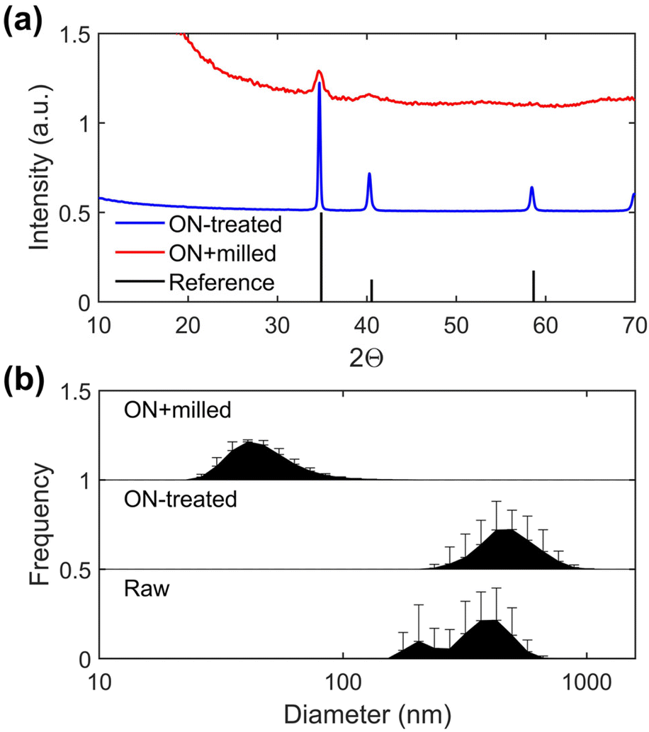 | ||
| Fig. 1 Production of TiH2 nanoparticle dispersion. (a) pXRD of powder following octylamine treatment and subsequent wet ball milling, with TiH2 reference (PDF 00-025-0982). (b) DLS size distributions following octylamine treatment and subsequent ball wet ball milling. | ||
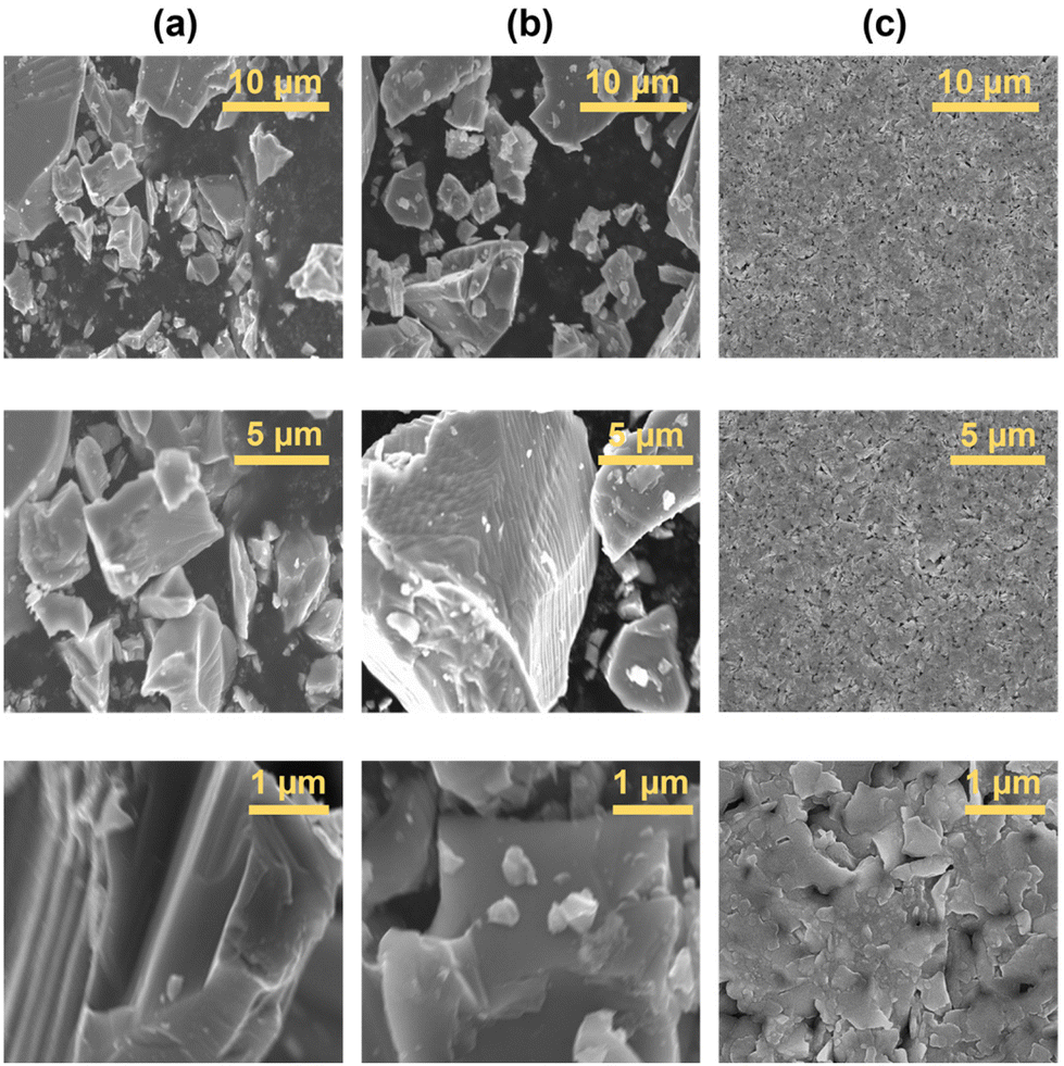 | ||
| Fig. 2 Scanning electron microscopy images showing progression of particle size during processing, including (a) raw TiH2 powder, (b) octylamine-treated powder, and (c) TiH2 nanoparticles following wet ball milling of octylamine-treated powder. | ||
Ink formulation and aerosol jet printing
AJP offers a digital, non-contact, high-resolution patterning capability with broad materials compatibility.36 Ultrasonic atomization of inks produces 1–5 μm droplets, which are transported to the printhead using a carrier gas stream. Within the printhead, an annular sheath gas surrounds the aerosol stream, narrowing the aerosol stream and preventing ink deposition on the interior of the nozzle. The aerosol stream is then directed through a deposition nozzle with a narrow orifice of 100–300 μm to produce high resolution patterns on the substrate (Fig. 3). To tailor the TiH2 dispersion for AJP, the cosolvent tetralin was added in a 4:1 v/v dispersion:tetralin ratio to mitigate droplet evaporation within the printhead.37 Tetralin offers similar chemical properties to the base solvent xylenes, does not significantly increase the viscosity, and has a lower vapor pressure to slow drying processes.
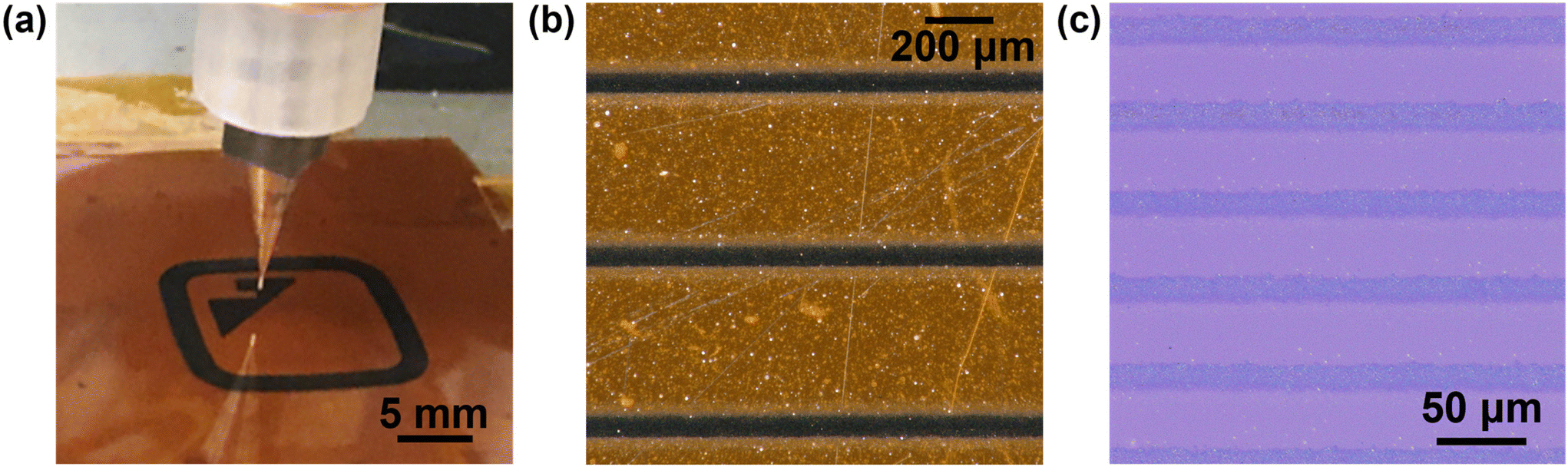 | ||
| Fig. 3 Aerosol jet printing of TiH2 nanoink. (a) Photograph of the print nozzle during patterning. (b and c) Optical microscopy images of dense lines on polyimide and high resolution lines on glass, respectively. | ||
During printing, the focusing ratio, defined as the sheath:carrier gas flow rate ratio, modulates the diameter of the aerosol beam, and thus the resolution.38 The print nozzle diameter is another key factor in determining the print resolution, and the sheath gas flow rate imposes a secondary effect on the deposition rate due to droplet impaction processes. To test the resolution capabilities for this ink, individual lines were printed and characterized (Fig. 3 and Fig. S1†). Several calibration tests were performed to quantitatively characterize the printing behavior of the TiH2 nanoink. First, the deposition rate was determined from the thickness of printed films at varying carrier gas flow rates (Fig. 4a). This study revealed a threshold flow rate of ∼6 sccm, below which little material deposition was observed. A fairly linear increase in film thickness or deposition rate with increasing flow rate (4.7(3) × 103 μm3 s−1 sccm−1) was observed, establishing a suitable range for printing. To study the resolution capabilities, traces were printed with three different nozzle sizes (233, 160 and 110 μm). The resulting resolution is shown in Fig. 4b, in which solid lines show baseline, ink-agnostic estimates of resolution, which largely track the measured values but show some important deviations.36 Using the 110 μm nozzle, a resolution as fine as 20 μm was achieved on both glass and polyimide substrates. In addition to deposition rate and resolution, print consistency is a key challenge for reliable AJP. In this case, a ∼50% decrease in the film thickness was observed during continuous printing over 5 h (Fig. S2†), which is attributed to reduced atomization resulting from a reduction in the ink volume within the cartridge.39 Despite this drift, the long 5 h time frame of continuous printing is notable for AJP,40 and does not indicate a limitation of the ink.
 | ||
| Fig. 4 Quantitative printing metrics. (a) Film thickness plotted against aerosol flow rate for a fixed focusing ratio, showing an approximately linear increase in deposition rate with a threshold of ∼6 sccm. (b) Line resolution as a function of focusing ratio for different nozzle sizes, showing resolution as fine as 20 μm. Solid lines in (b) correspond to a theoretical calculation of the nominal ink stream width exiting the nozzle. | ||
Photonic curing
A key challenge for metal-based inks is the identification of a suitable post-processing treatment that results in an electrically continuous, functional network from individual printed particles. This is particularly challenging for this system, given the susceptibility of titanium-based materials to oxidation at high temperatures. Previous efforts to post-process pastes containing TiH2 deposited by extrusion printing to Ti metal (Ti0) required debinding (200–300 °C), high temperature (600 °C) dehydriding under high vacuum, and subsequent high temperature sintering (1050 °C), conditions unsuitable for flexible plastic substrates.26 To explore an alternative curing method, intense pulsed light (IPL) processing was studied. This method uses a broadband pulsed light source (commonly a Xe flash lamp) to produce a high intensity (∼1–10 kW cm−2), short (∼1 ms) light pulse.34,41,42 This has been previously applied to a diverse range of nanomaterials, including silver, copper, graphene, silicon, and semiconducting and piezoelectric metal oxides.43–49 This light pulse is selectively absorbed in the TiH2 film, leading to rapid heating to high temperatures that will sinter the nanoparticle traces while limiting thermal damage to the substrate.Prior to IPL curing, printed TiH2 films have a black appearance with a uniform microstructure of TiH2 nanoparticles and polymer binder, as shown in Fig. 5a and b. Upon exposure to the high energy light pulse, a visible transformation was observed, resulting in a gray film with a metallic luster and clear microstructural evolution, as shown in Fig. 5c and d. SEM images of the traces reveal a porous, high surface area microstructure, with evidence of sintered primary particles. This is likely a result of the rapid nature of the photonic curing process and the release of gaseous species upon decomposition or conversion of the dispersant, ligands, and TiH2. While not suitable for dense, highly conductive lines, anticipated applications of this material are distinct from traditional conductors such as silver. For many applications that exploit the electrochemical stability and biocompatibility of titanium-based compounds (e.g., energy, catalysis, sensing, biomedical), this high surface area morphology is advantageous.23,24,50
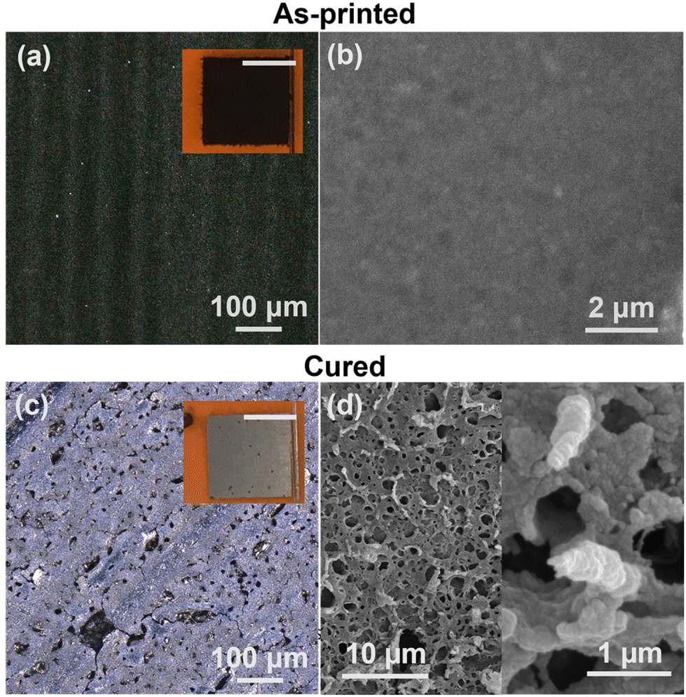 | ||
| Fig. 5 Morphology of the print TiH2, including (a and c) optical and (b and d) SEM imaging for as-printed (a and b) and photonically cured (c and d) films. | ||
Chemical and electrical characterization
Insights into the chemical changes occurring during IPL curing are provided by more in depth characterization. Fourier-transform infrared spectroscopy (FTIR) of samples prior to photonic curing show clear bends and stretches associated with the dispersant, particularly in the 2800–3000 cm−1 range (Fig. 6a). Following photonic curing, no evidence of these stretches/bends is present, with the weak peaks remaining attributed to the polyimide substrate. Prior to curing, pXRD patterns indicated the presence of peaks associated with TiH2 (PDF 00-025-0982); after the photonic curing process, these peaks are present but less distinct (Fig. 6b), suggesting that at least some TiH2 remains.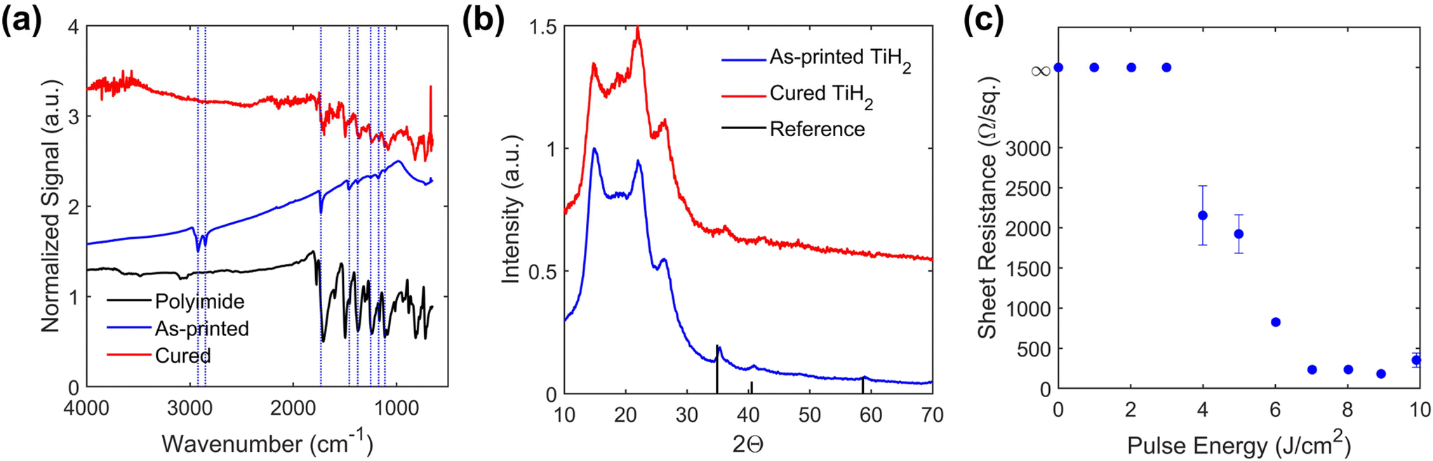 | ||
| Fig. 6 Analysis of the photonic curing process, including (a) FTIR, (b) pXRD, and (c) electrical sheet resistance for TiH2 films before and after IPL curing. Reference pXRD peaks in (b) correspond to PDF 00-025-0982. | ||
For a systematic test, pulse energies of 1–10 J cm−2 were applied in 1 J cm−2 increments, leading to expected heating above 1000 °C (Fig. S3†).51 As the pulse energy was increased, the electrical sheet resistance shows a transition from 3–7 J cm−2 as the nonconductive, as-printed film is sintered to achieve a typical sheet resistance of ∼200 Ω □−1 for pulse energies of 7–9 J cm−2 (Fig. 6c). This method therefore allows curing on polyimide substrates, which is not possible using conventional thermal annealing. Indeed, thermal curing of patterns on silicon wafers required a temperature as high as 800 °C under nitrogen to yield comparable electrical properties (Fig. S4†). Moreover, the efficacy of photonic curing appears to be independent of the process environment, with similar results observed following curing under H2/N2, light vacuum, and air.
While single-pulse IPL curing is effective, it can lead to a porous microstructure and limited adhesion that impacts bending tolerance (Fig. S5†). In this case, multiple pulses can provide an effective means to improve electrical properties and tailor the final morphology. While the initial light pulse likely decomposes the organic constituents, leading to gas evolution and pore formation, the second pulse reheats the remaining material to close pores. This multi-pulse process can lead to improved electrical performance, with a sheet resistance as low as ∼150 Ω □−1, a more lustrous visual appearance, and a denser film morphology (Fig. S4 and S6†).
Conclusions
In this work, a simple TiH2 nanoink was developed as an alternative conductor for printed electronic applications. This approach broadens the scope of printable materials beyond traditional, oxidation-resistant coinage metals, making more diverse functional properties accessible. Future extension to metal hydrides beyond titanium will further expand the palette of materials compatible with printed electronics, particularly considering the ability to chemically convert and alloy hydride precursors. Commercial TiH2 powder with 1–10 μm particles was first treated at elevated temperature with ON, followed by wet ball milling in the presence of a dispersant to produce TiH2 nanoparticles. Aerosol jet printing of a nanoink prepared from this dispersion was demonstrated, achieving controllable patterning with a resolution as fine as 20 μm. Following printing, IPL curing was used to convert the nanoparticle film into a continuous, conductive network. The photonic curing conditions are shown to influence film microstructure, varying from a porous, high surface area morphology to more dense films for single- and multi-pulse curing, respectively. Moreover, the porous microstructure could find potential use in energy, catalysis, and sensing applications. Overall, this marks a novel approach to conductive ink design for high resolution digital patterning, providing an alternative class of printed materials to expand the scope of opportunities for printed electronics.Author contributions
Conceptualization: TJB, EBS, NSB; data curation: EBS, RRT, TJB; analysis: EBS, TJB, NSB; funding: TJB, EBS; investigation: TJB, NSB, EBS, RRT, THN, MPR; methodology: TJB, NSB, EBS; writing – original: EBS, RRT, TJB, NSB; writing – review: EBS, TJB, NSB.Conflicts of interest
There are no conflicts to declare.Acknowledgements
This work was supported by the Laboratory Directed Research and Development Program at Sandia National Laboratories. Dr E. B. Secor was supported in part by the Harry S. Truman Fellowship. The authors would like to acknowledge Ms S. Dickens, Mr P. Reuel and Dr B. Kaehr for assistance with SEM imaging, along with Dr B. A. Hernandez-Sanchez for assistance with pXRD analysis. Sandia National Laboratories is a multi-program laboratory managed and operated by National Technology and Engineering Solutions of Sandia, LLC., a wholly owned subsidiary of Honeywell International, Inc., for the U.S. Department of Energy's National Nuclear Security Administration under contract DE-NA-0003525. This paper describes objective technical results and analysis. Any subjective views or opinions that might be expressed in the paper do not necessarily represent the views of the U.S. Department of Energy or the United States Government.References
- K. Fukuda and T. Someya, Adv. Mater., 2017, 29, 1602736 CrossRef PubMed.
- D. Lupo, W. Clemens, S. Breitung and K. Hecker, in Applications of organic and printed electronics: a technology-enabled revolution, ed. E. Cantatore, Springer, New York, 2013, pp. 1–26 Search PubMed.
- P. Sarobol, A. Cook, P. G. Clem, D. Keicher, D. Hirschfeld, A. C. Hall and N. S. Bell, Annu. Rev. Mater. Res., 2016, 46, 41–62 CrossRef CAS.
- Y. S. Rim, S. Bae, H. Chen, N. De Marco and Y. Yang, Adv. Mater., 2016, 28, 4415–4440 CrossRef CAS PubMed.
- R. Abbel, Y. Galagan and P. Groen, Adv. Eng. Mater., 2018, 20, 1701190 CrossRef.
- L. J. Deiner and T. L. Reitz, Adv. Eng. Mater., 2017, 19, 1600878 CrossRef.
- A. Kamyshny and S. Magdassi, Small, 2014, 10, 3515–3535 CrossRef CAS.
- E. Dimitriou and N. Michailidis, Nanotechnology, 2021, 32, 502009 CrossRef CAS PubMed.
- N. C. Raut and K. Al-Shamery, J. Mater. Chem. C, 2018, 6, 1618–1641 RSC.
- H. T. Phan and A. J. Haes, J. Phys. Chem. C, 2019, 123, 16495–16507 CrossRef CAS.
- S. Magdassi, M. Grouchko and A. Kamyshny, Materials, 2010, 3, 4626–4638 CrossRef CAS PubMed.
- W. Wu, Nanoscale, 2017, 9, 7342–7372 RSC.
- G. Kotzar, M. Freas, P. Abel, A. Fleischman, S. Roy, C. Zorman, J. M. Moran and J. Melzak, Biomaterials, 2002, 23, 2737–2750 CrossRef CAS PubMed.
- K. T. Chiang and L. Yang, Corrosion, 2010, 66, 095002 CrossRef.
- C. J. Zhang, S. Pinilla, N. McEvoy, C. P. Cullen, B. Anasori, E. Long, S.-H. Park, A. Seral-Ascaso, A. Shmeliov, D. Krishnan, C. Morant, X. Liu, G. S. Duesberg, Y. Gogotsi and V. Nicolosi, Chem. Mater., 2017, 29, 4848–4856 CrossRef CAS.
- C. Zhang, L. McKeon, M. P. Kremer, S.-H. Park, O. Ronan, A. Seral-Ascaso, S. Barwich, C. Ó. Coileáin, N. McEvoy, H. C. Nerl, B. Anasori, J. N. Coleman, Y. Gogotsi and V. Nicolosi, Nat. Commun., 2019, 10, 1795 CrossRef PubMed.
- M. Borghetti, M. Serpelloni, E. Sardini, D. Spurling and V. Nicolosi, Sens. Actuators, A, 2021, 332, 113185 CrossRef CAS.
- X. Wang, Z. Zhang, B. Tang, N. Lin, H. Hou and Y. Ma, J. Power Sources, 2013, 230, 81–88 CrossRef CAS.
- M. Weder, D. Hegemann, M. Amberg, M. Hess, L. Boesel, R. Abächerli, V. Meyer and R. Rossi, Sensors, 2015, 15, 1750–1759 CrossRef CAS.
- S. Sartori, F. Cuevas and M. Latroche, Appl. Phys. A, 2016, 122, 135 CrossRef.
- Y. Oumellal, W. Zaïdi, J.-P. Bonnet, F. Cuevas, M. Latroche, J. Zhang, J.-L. Bobet, A. Rougier and L. Aymard, Int. J. Hydrogen Energy, 2012, 37, 7831–7835 CrossRef CAS.
- C. E. Sanders, D. Verreault, G. S. Frankel and H. C. Allen, J. Electrochem. Soc., 2015, 162, C630–C637 CrossRef CAS.
- J. M. McEnaney, S. J. Blair, A. C. Nielander, J. A. Schwalbe, D. M. Koshy, M. Cargnello and T. F. Jaramillo, ACS Sustainable Chem. Eng., 2020, 8, 2672–2681 CrossRef CAS.
- A. Gao, R. Hang, L. Bai, B. Tang and P. K. Chu, Electrochim. Acta, 2018, 271, 699–718 CrossRef CAS.
- B. Y. Ahn, D. Shoji, C. J. Hansen, E. Hong, D. C. Dunand and J. A. Lewis, Adv. Mater., 2010, 22, 2251–2254 CrossRef CAS.
- E. Hong, B. Y. Ahn, D. Shoji, J. A. Lewis and D. C. Dunand, Adv. Eng. Mater., 2011, 13, 1122–1127 CrossRef CAS.
- J. M. Hoey, A. Lutfurakhmanov, D. L. Schulz and I. S. Akhatov, J. Nanotechnol., 2012, 2012, 1–22 CrossRef.
- K. Hong, Y. H. Kim, S. H. Kim, W. Xie, W. D. Xu, C. H. Kim and C. D. Frisbie, Adv. Mater., 2014, 26, 7032–7037 CrossRef CAS PubMed.
- A. Mette, P. L. Richter, M. Hörteis and S. W. Glunz, Prog. Photovolt.: Res. Appl., 2007, 15, 621–627 CrossRef CAS.
- M. S. Saleh, C. Hu and R. Panat, Sci. Adv., 2017, 3, e1601986 CrossRef.
- R. R. Salary, J. P. Lombardi, D. L. Weerawarne, P. K. Rao and M. D. Poliks, Additive Manufacturing; Manufacturing Equipment and Systems; Bio and Sustainable Manufacturing, American Society of Mechanical Engineers, Erie, Pennsylvania, USA, 2019, vol. 1, p. V001T01A035 Search PubMed.
- J. B. Andrews, C. Cao, M. A. Brooke and A. D. Franklin, IEEE Sens. J., 2017, 17, 4612–4618 CAS.
- C. Hollar, Z. Lin, M. Kongara, T. Varghese, C. Karthik, J. Schimpf, J. Eixenberger, P. H. Davis, Y. Wu, X. Duan, Y. Zhang and D. Estrada, Adv. Mater. Technol., 2020, 5, 2000600 CrossRef CAS PubMed.
- K. Schroder, S. McCool and W. Furlan, NSTI Nanotech 2006 Technical Proceedings, CRC Press, 2006, vol. 3, pp. 198–201 Search PubMed.
- S. D. Bunge and T. J. Boyle, US Pat., US6929675B1, 2005 Search PubMed.
- E. B. Secor, Flexible Printed Electron., 2018, 3, 035002 CrossRef.
- E. B. Secor, Flexible Printed Electron., 2018, 3, 035007 CrossRef.
- A. Mahajan, C. D. Frisbie and L. F. Francis, ACS Appl. Mater. Interfaces, 2013, 5, 4856–4864 CrossRef CAS.
- R. R. Tafoya and E. B. Secor, Flexible Printed Electron., 2020, 5, 015009 CrossRef CAS.
- M. Smith, Y. S. Choi, C. Boughey and S. Kar-Narayan, Flexible Printed Electron., 2017, 2, 015004 CrossRef.
- D. Angmo, T. T. Larsen-Olsen, M. Jørgensen, R. R. Søndergaard and F. C. Krebs, Adv. Energy Mater., 2013, 3, 172–175 CrossRef CAS.
- J. Perelaer, R. Abbel, S. Wünscher, R. Jani, T. van Lammeren and U. S. Schubert, Adv. Mater., 2012, 24, 2620–2625 CrossRef CAS PubMed.
- E. Drahi, S. Blayac, A. Borbely and P. Benaben, Thin Solid Films, 2015, 574, 169–176 CrossRef CAS.
- B. L. Greenberg, Z. L. Robinson, K. V. Reich, C. Gorynski, B. N. Voigt, L. F. Francis, B. I. Shklovskii, E. S. Aydil and U. R. Kortshagen, Nano Lett., 2017, 17, 4634–4642 CrossRef CAS PubMed.
- H. S. Lim, S. J. Kim, H. W. Jang and J. A. Lim, J. Mater. Chem. C, 2017, 5, 7142–7160 RSC.
- J. Ouyang, D. Cormier, S. A. Williams and D. A. Borkholder, J. Am. Ceram. Soc., 2016, 99, 2569–2577 CrossRef CAS.
- M. S. Rager, T. Aytug, G. M. Veith and P. Joshi, ACS Appl. Mater. Interfaces, 2016, 8, 2441–2448 CrossRef CAS PubMed.
- E. B. Secor, B. Y. Ahn, T. Z. Gao, J. A. Lewis and M. C. Hersam, Adv. Mater., 2015, 27, 6683–6688 CrossRef CAS PubMed.
- P. Gokhale, D. Mitra, E. Sowade, K. Y. Mitra, H. L. Gomes, E. Ramon, A. Al-Hamry, O. Kanoun and R. R. Baumann, Nanotechnology, 2017, 28, 495301 CrossRef PubMed.
- U. Michaelidou, A. ter Heijne, G. J. W. Euverink, H. V. M. Hamelers, A. J. M. Stams and J. S. Geelhoed, Appl. Environ. Microbiol., 2011, 77, 1069–1075 CrossRef CAS PubMed.
- M. J. Guillot, S. C. McCool and K. A. Schroder, Fluids and Heat Transfer, Parts A, B, C, and D, American Society of Mechanical Engineers, Houston, Texas, USA, 2012, vol. 7, pp. 19–27 Search PubMed.
Footnote |
| † Electronic supplementary information (ESI) available: Fig. S1–S6 (PDF). See DOI: https://doi.org/10.1039/d2nr03571e |
| This journal is © The Royal Society of Chemistry 2022 |