
Inverse size-dependent Stokes shift in strongly quantum confined CsPbBr3 perovskite nanoplates†
Amit
Vurgaft
a,
Rotem
Strassberg
 a,
Reut
Shechter
b,
Rachel
Lifer
b,
Jakob C.
Dahl
cd,
Emory M.
Chan
d and
Yehonadav
Bekenstein
*ab
a,
Reut
Shechter
b,
Rachel
Lifer
b,
Jakob C.
Dahl
cd,
Emory M.
Chan
d and
Yehonadav
Bekenstein
*ab
aThe Solid-State Institute, Technion – Israel Institute of Technology, 32000 Haifa, Israel
bDepartment of Materials Science and Engineering, Technion-Israel Institute of Technology, Haifa 32000, Israel. E-mail: bekenstein@technion.ac.il
cDepartment of Chemistry, University of California, Berkeley, California 94720, USA
dMolecular Foundry, Lawrence Berkeley National Laboratory, Berkeley, California 94720, USA
First published on 15th November 2022
Abstract
Colloidal semiconductor nanocrystals (NCs) are used as bright chromatic fluorophores for energy-efficient displays. We focus here on the size-dependent Stokes shift for CsPbBr3 nanocrystals. The Stokes shift, i.e., the difference between the wavelengths of absorption and emission maxima, is crucial for display application, as it controls the degree to which light is reabsorbed by the emitting material reducing the energetic efficiency. One major impediment to the industrial adoption of NCs is that slight deviations in manufacturing conditions may result in a wide dispersion of the product's properties. A data-driven analysis of over 2000 reactions comparing two data sets, one produced via standard colloidal synthesis and the other via high-throughput automated synthesis is discussed. We show that differences in the reaction conditions of colloidal CsPbBr3 nanocrystals yield nanocrystals with opposite Stokes shift size-dependent trends. These match the morphologies of two-dimensional nanoplatelets (NPLs) and nanocrystal cubes. The Stokes shift size dependence trend of NPLs and nanocubes is non-monotonic indicating different physics is at play for the two nanocrystal morphologies. For nanocrystals with cubic shape, with the increase of edge length, there is a significant decrease in Stokes shift values. However, for NPLs with the increase of thickness (1–4 ML), Stokes shift values will increase. The study emphasizes the transition from a spectroscopic point of view and relates the two Stokes shift trends to 2D and 0D exciton dimensionalities for the two morphologies. Our findings highlight the importance of CsPbBr3 nanocrystal morphology for Stokes shift prediction.
 Yehonadav Bekenstein | Dr Yehonadav Bekenstein is an assistant professor of materials science and engineering and the solid-state institute at Technion, Israel's institute of technology. Yehonadav completed his physics and chemistry degrees at the Hebrew University of Jerusalem receiving his Ph.D. in 2015. Following this, he spent three years at the University of California, Berkeley as a Rothschild Fellow, working with Prof Alivisatos. Since 2018, he heads an independent research group, holding an ERC Starting Grant (Heteroplates). His major research interest is discovering new materials and designing their properties for the benefit of mankind. His current focus is excitonic collective interactions in perovskite nanocrystals. |
Introduction
Colloidal synthesis is a cost-effective method enabling the scalable fabrication of quantum dots with size-dependent quantum-confined excitons. However, even slight variations in the parameters of wet synthetic methods may introduce a large variety of particle dimensions, morphologies, compositions, and consequently different optical properties of the obtained nanocrystal. Eliminating variety and achieving uniform properties is of interest to the display industry to obtain more consistent, high-quality products.1–4Years of scientific development on the synthesis of model quantum dot materials have resulted in fine control over their critical physical parameters, facilitating their implementation into a commercial technology. For example, CdSe/CdS5–8 and InP/ZnS9,10 have been optimized for use in the display industry. Lead halide perovskite nanocrystals have earned worldwide attention since they exhibited excellent photophysical properties, including high photoluminescence quantum yields (PLQY ∼ 50–90%), narrow emission linewidth (70–140 meV), broad absorption, and tunable emission in the entire visible range.11–13 All-inorganic lead halide perovskites have demonstrated exceptional photovoltaic14 and optoelectronic properties, leading to their incorporation into solar cells,15 light-emitting diodes, photodetectors, waveguides, and lasers.16,17 Recent studies on the electronic structure of perovskite quantum dots and defect tolerance are emerging.18–20 However, there are still debates on the underlying photophysical properties and the nature of the emitting state.
Stokes shift, the difference between absorbing and emitted energies, is a general phenomenon for fluorophores and is associated with energy dissipation via vibrational modes. Predicting Stokes shifts of fluorophores for the display industry is crucial, as a measure of the degree of reabsorption of light by the emitter which influences reabsorption losses and device energetic efficiencies.21–23 For nanocrystals the dependence of Stokes shift on NCs size was first observed in colloidal CdSe quantum dots.24,25 Efros et al. showed that the Stokes shifts may vary between ∼100 to 10 meV for particle diameters between ∼1 and 5 nm. For CsPbBr3, a size-dependent Stokes shift has been studied,26,27 specifically in the cubic morphology revealing the existence of an inherent, size-dependent, confined hole state 260 to 70 meV above the valence band edge state.28
Colloidal synthesis of CsPbBr3 was studied intensively in past years,13 the fast metastasis and the delicate equilibria29 between ligands and intermediate products result in a complex dependence on the reaction concentrations and conditions. Especially challenging is the synthesis of pure phases of very small monodispersed nanocubes. These are usually accompanied by other morphologies such as nanoplates and lead halide complexes. Previous systematic exploration of the Cs–Pb–Br synthesis space was conducted via a high-throughput automated synthesis by Dahl et al.30 The study portrayed the formation reactions under varying starting conditions generating vast amounts of data on the precursors, intermediates, and products. However, such an approach was limited by cleaning steps using a centrifuge. In this study, we, therefore, complemented the data with results from many standard manual reactions we conducted.
To analyze this vast amount of data and get a clear understanding of Stokes shift engineering and rational selection of starting conditions we utilize a data-driven approach.
We have cleaned and analyzed UV-Vis absorption and emission data from both datasets using statistical methods. The first dataset is a collection of 672 manual syntheses, and its preparation process is extensively explained in the Experimental section. Most of the syntheses were made using oleic acid ligands, but additional samples of other ligands were also present. These syntheses aimed to produce a pure single phase of the CsPbBr3 perovskites complemented by a cleaning step using a centrifuge. The second dataset is based on a high-throughput automated synthesis by Dahl et al.30 The aim of that study was to explore the chemical parameter space of the Cs–Pb–Br nanocrystal system and factorial sets of 1351 automated experiments were performed on a synthesis robot. The resulting samples contained a mixture of phases of the Cs–Pb–Br space, including non-perovskite phases. For this study, we have selected only those products which show significant fractions of perovskite phase products.
Spectroscopic studies of nanocrystals produced by the two synthetic methods show that the size-dependent Stokes shift between nanoplates and nanocubes is non-monotonic and even not continuous when reaching the nanoplate regime. This non-monotonic trend originates from the quantum and dielectric confinement effect, which plays a significant role in 2D and intermediate (2D/3D) materials. Size-dependent Stokes shift was discussed by Brennan et al. for cubes,26 and here we compare and extend this model also to two-dimensional nanoplates.
Experimental section
Manual synthesis
Lead oleate preparation. 380 mg (1 mmole) lead acetate trihydrate powder was mixed with 1.6 ml (5 mmol) OA. The sample was heated for 4 hours while stirring at 100 °C until no bubbles were apparent and a light yellow-brown color ensures complete solubilization of the lead powder in the OA. The solution was briefly reheated before synthesis to ensure dissolution and thorough mixing of precursors.
Preparation for synthesis with ODA. 41 mg (1.52 mmol) of ODA powder was mixed with 2.4 m hexane for half an hour before synthesis. The rest of the synthesis was made as mentioned below without adding the amine source.
Single monolayer NPLs synthesis. In a typical synthesis, 37.5 μl of OA, 1.52 mmol of alkylamine ligand, 25 μl of lead precursor (0.0156 mmol) were mixed and diluted with 2.35 ml hexane in an 8 ml vial, at room temperature. 38 μl of benzoyl bromide (0.32 mmol) was added to perform the reaction. Then, after about 10 seconds, a white translucent solution was observed, and the solution became turbid. The synthetic mixture was centrifuged at 10k rpm for 10 min to obtain the precipitate solution. After centrifuge, the precipitate was redispersed in 3 ml hexane for characterization and future use.
Cesium oleate precursor preparation. 19.3 mg (0.06 mmol) of cesium carbonate powder was dissolved in 10 mL of OA at 100 °C under continuous stirring. After 1 hour, the solution was cooled down to room temperature and stored for further use.
Lead bromide precursor preparation. 36.7 mg (0.1 mmol) of lead bromide powder (PbBr2) was dissolved in 10 mL of toluene with 100 μl of OLA and 100 μl of OA at 100 °C under continuous stirring. After 1 hour, the solution was cooled to room temperature and stored for further use.
Synthesis of CsPbBr3 NPLs. To control their thickness, a certain amount of Cs–oleate precursor (10 μl–3 ml) was added to 1 ml of lead bromide solution under vigorous stirring. After 5 s, 1 ml of acetone was added into the solution as an anti-solvent. After 1 min of stirring, the solution was centrifuged at 4000 rpm for 3 min. The precipitate was redispersed in 2 ml of hexane.
Results & discussion
Data preprocessing
To compare the Stokes shift of manual and automated datasets, we review the records of the concentrations of precursors, the emission and absorption spectra, and the fractions of the different CsPbBr3 product morphologies. Fig. 1a, b and c show representative TEM images of the different NCs morphologies, nanocubes, and nanoplates (NPLs) ensembles from the manual dataset, correspondingly. Absorption and emission spectra of selected samples from the automated dataset are presented in Fig. 1d. As expected, the emission peaks are shifted from the band edge exciton state.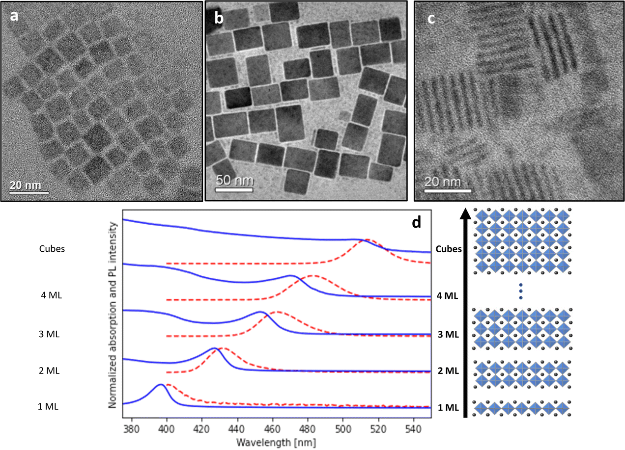 | ||
| Fig. 1 TEM and spectroscopy of nanocubes and NPLs. TEM micrographs of CsPbBr3 nanocubes (a) and NPLs (b and c). Absorption (solid blue lines) and emission (dashed red lines) spectra of ensembled CsPbBr3 NCs, corresponding to 1, 2, 3, 4 ML and cubes (d). | ||
The first step of data analysis was to fit the emission and absorption spectra to Gaussian functions using automatic curve algorithms, to extract the corresponding Stokes Shift (examples can be seen in Fig. S2†). For the manual dataset, labeling of emission and absorption peaks was straightforward due to the uniformity of the samples after purification via centrifuge. The automated datasets demanded further statistical cleaning. This is since the products were not purified by centrifuge and contain a distribution of nanoplatelet thickness (see Fig. S2†). The fraction of the multiple morphologies of Cs–Pb–Br space was determined using deconvolution of the absorption spectra (for details see our previous work).30
We only use samples with a fraction higher than 0.82 with a specific emission line corresponding to homogenous thickness distribution. Finally, after these data filtering steps, we summarized the spectroscopic absorption and emission measurements from 212 “winning” samples in the automated dataset (Table 1) and 256 samples in the manual dataset (Table 2). The dataset is separated into regions according to different morphologies of the samples: 1, 2, 3, 4 ML, and nanocubes with increasing wavelength.
| Morphology | E ab [eV] | Count | Absorbance [eV] | Emission [eV] | Stokes shift [meV] | |||
|---|---|---|---|---|---|---|---|---|
| Mean | Std | Mean | Std | Mean | Std | |||
| 1 ML | (3, 3.2] | 2 | 3.12 | 0 | 3.09 | 0 | 31.3 | 0 |
| 2 ML | (2.8, 3] | 134 | 2.89 | 0.02 | 2.86 | 0.03 | 25.4 | 10.3 |
| 3 ML | (2.7, 2.8] | 45 | 2.74 | 0.02 | 2.69 | 0.02 | 49.5 | 22.3 |
| 4 ML | (2.58, 2.7] | 18 | 2.64 | 0.02 | 2.56 | 0.03 | 76.6 | 17.4 |
| Cubes | (2.53, 2.58] | 3 | 2.56 | 0.02 | 2.48 | 0.02 | 70.3 | 4.2 |
| (2.5, 2.53] | 0 | |||||||
| (2.48, 2.5] | 3 | 2.49 | 0.01 | 2.44 | 0.003 | 55.6 | 4.4 | |
| (2.46, 2.48] | 2 | 2.47 | 0.01 | 2.43 | 0.01 | 40.4 | 2.9 | |
| (2.43, 4.46] | 3 | 2.45 | 0.005 | 2.41 | 0.002 | 35.7 | 3.3 | |
| (2.41, 2.43] | 2 | 2.42 | 0.01 | 2.40 | 0.004 | 19.5 | 2.8 | |
| Total | 212 | |||||||
| Morphology | E ab [eV] | Count | Absorbance [eV] | Emission [eV] | Stokes shift [meV] | |||
|---|---|---|---|---|---|---|---|---|
| Mean | Std | Mean | Std | Mean | Std | |||
| 1 ML | (3, 3.2] | 132 | 3.12 | 0.03 | 3.06 | 0.03 | 62.5 | 16.7 |
| 2 ML | (2.8, 3] | 35 | 2.89 | 0.03 | 2.81 | 0.04 | 78.2 | 18.3 |
| 3 ML | (2.7, 2.8] | 60 | 2.76 | 0.03 | 2.69 | 0.03 | 68.7 | 12.4 |
| 4 ML | (2.58, 2.7] | 5 | 2.67 | 0.02 | 2.60 | 0.01 | 71.8 | 9.7 |
| Cubes | (2.53, 2.58] | 1 | 2.57 | 2.51 | 64.6 | |||
| (2.5, 2.53] | 1 | 2.52 | 2.46 | 53.3 | ||||
| (2.48, 2.5] | 0 | |||||||
| (2.46, 2.48] | 0 | |||||||
| (2.43, 4.46] | 0 | |||||||
| (2.41, 2.43] | 3 | 2.42 | 0.01 | 2.38 | 0.002 | 43.1 | 3.5 | |
| (2.38, 2.41] | 5 | 2.39 | 0.004 | 2.36 | 0.007 | 26.5 | 6.4 | |
| (2.1, 2.38] | 13 | 2.38 | 0.005 | 2.36 | 0.009 | 12.6 | 9.1 | |
| Total | 256 | |||||||
The Stokes shift of the automated dataset with a phase fraction more significant than 0.82 and manual dataset were plotted versus the typical absorption (emission) energy, as shown in Fig. 2a and b (Fig. S5a and b†), respectively. The same trend can be seen in both datasets for the cube morphology, in which the average Stokes shift values decrease from 70 to 10 meV with increasing nanocube size. However, for the NPLs regime, there is an increase from 20 to 70 meV with increasing NPLs thickness from 1 to 4 ML (automated dataset). But for the manual dataset, the NPLs Stokes shift values stay constant at approximately 70 meV. The above are averaged values while in practice there is a statistical spread around the typical absorption wavelength for all morphologies.32,33 For NPLs, the thickness is atomically defined and there is little inhomogeneity. The observed statistical variance is due to the NPLs lateral size inhomogeneity and inconsistent surface passivation due to the dynamic nature of the ligand.34
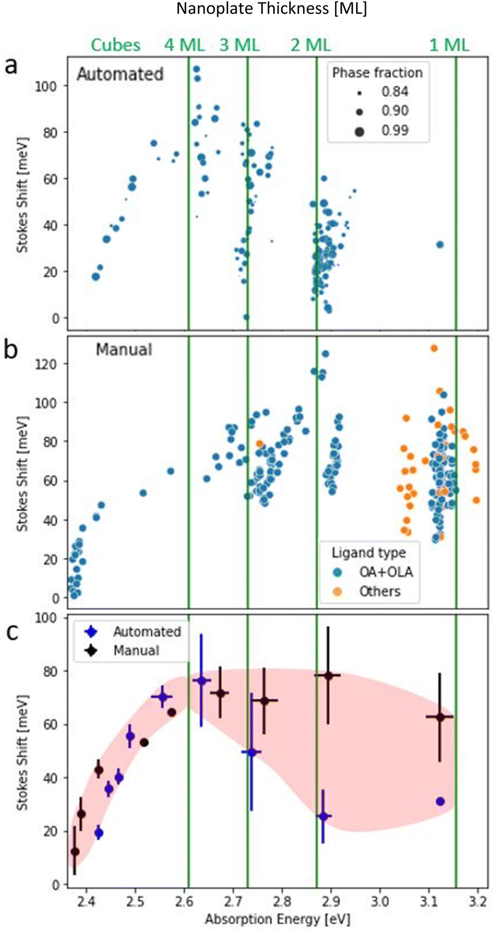 | ||
| Fig. 2 Size dependent Stokes shift. Solid lines refer to the absorption energy, which corresponds to reported values of 1, 2, 3, and 4 ML.32,33 Stokes shift versus the absorbance energy in the automated dataset. The size of the data point corresponds to the maximal fraction of the phase in the sample (a). Stokes shift versus the absorbance energy in the manual dataset. The color of the datapoint refers to ligand type (b). Averaged results of Stokes shift versus the absorption energy for automated (blue) and manual (black) datasets as well (c). | ||
Another ligand-based effect can be seen in the manual dataset, a minority of the 1 ML samples were prepared using shorter ligands than oleic acids, such as butylamine or unsaturated chain octadecylamine. These variations result in a blue/red shift of both emission and absorption peaks (Fig. 2b). However, this shift does not affect the value of Stokes shift since it affects the absorption and emission in a similar way.
We note in passing that the clusters in Fig. 2a and b have a slight slope, which creates a form of parallel stripes in the NPLs region. Moreover, the slopes at the absorption figure are opposite to the slopes at the emission (Fig. S4 and S5a and b†). The reason for this slope is not intrinsic. Instead, it comes from the definition of Stokes shift and its mathematical dependence of the emission and the absorption wavelengths, i.e.:
| ΔEs = Eabs − Eem. | (1) |
In eqn (S4) and (S5)† we show that the slopes follow this dependence for each cluster locally. In addition, the slopes at the emission and the absorption figures are opposite, simply due to the sign of the corresponding term in the Stokes shift equation (eqn (1)). In Fig. S6 and S7† a standard deviation of 9 to 16 meV in the Stokes shift stems from the fact that emission data was extracted from experimental results, and encompasses an instrument measurement error. Such deviation of the absorption and emission wavelength directly affects the extent of the variance portrayed in the slopes (Fig. 2a and b).
To understand the behavior of each cluster, we summarized the Stokes shift values for both datasets. Fig. 2c compares the Stokes shift in NPLs and nanocubes. With the increase of absorption wavelength (i.e., the size of the NCs), the trend of Stokes shift is negative for cubes in both datasets. However, for NPLs, we can see a positive increase in Stokes shift for the automated method. Whereas in the manual method values are distributed around 70 meV. In both datasets there are significant error bars (<35 meV), which originate from concentration and reabsorption effects24,28 (see Fig. S8c†). However, these do not obscure the different observed trends for cubes and nanoplates.
Two control measurements and analysis further reassure our observations. First, two different solvents were tested (ODE, hexane) with no significant effect beyond that of the concentration mentioned earlier (Fig. S8a and b†).
It is important to note that usage of only high purity fraction data does not statistically shift our results as shown in the analysis in ESI (Fig. S9†). Stokes shift values for full fraction samples are within the average value of the Stokes shift of the mixed fraction samples.
To better understand the origin of the two different Stokes shift trends nanocubes vs. nanoplates we examine current theoretical modeling. The general expression for the band edge excitonic energy is defined as:35,36
| Ex = Eg + (Ee + Eh) − Ec − Bx | (2) |
In eqn (2), Eg is the bulk bandgap, Ee and Eh represent the kinetic energy of the electron and hole, respectively, while Ec is the energy of their Coulomb attraction. The last term, Bx, is the exciton binding energy associated with the relative motion of the electron and hole. For the different CsPbBr3 morphologies, NPLs and cubes, these terms result from different physical effects.37 We split our analysis into two parts: the cube-shaped NCs and NPLs. Parameters and equations used for the following analysis are shown in Table S1.† Since the physical models depend on L, the edge length of the NCs, a transformation of the absorption wavelength to the edge length was carried out. For NPLs, each number of layers n has its distinct absorption and emission peaks, and the thickness is simply L = n·0.6[nm], where n is number of layers and 0.6 nm is the unit cell thickness. For cubes, we used approximated values according to previous results of Brennan et al.27 (Fig. S10†). For reference, we compare our analysis to experimental data in studies of Bernnan et al.27 and Protesescu et al.11 for the cube shaped NCs, and to Bekenstein et al.32 and Bohn et al.33 for the NPL morphology. As can be seen in Fig. 3a, the trend of the excitonic energy for the cubes and NPLs is not continuous, there is an energy decrease of ∼0.25 eV at an edge length of 4 nm. In order to understand the discontinuous trend of the exciton energy, we compared our experimental excitonic energy to theoretical models by Efros et al.38,39
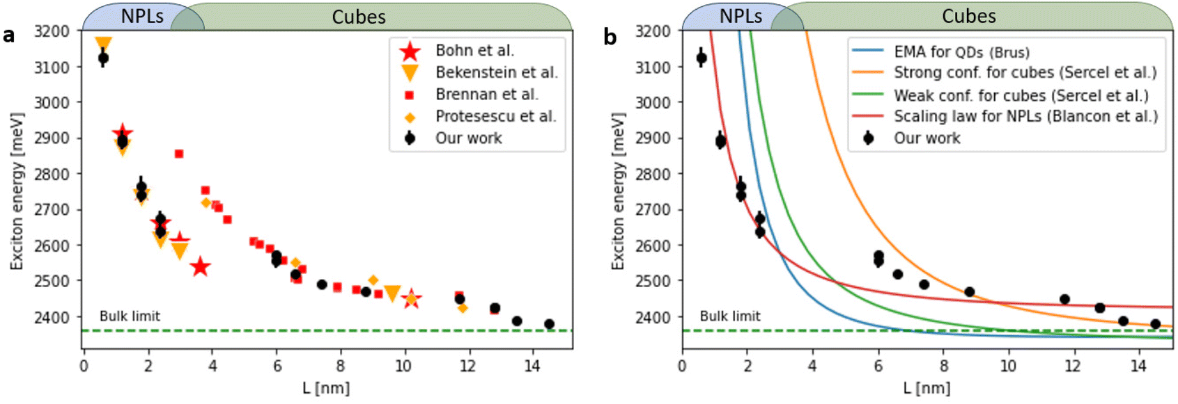 | ||
| Fig. 3 Exciton energy of cubes and NPLs as compared to previous research. Experimental automated and manual exciton energies compared to those extracted from existing literature (a) and to theoretical models (b) for cubes and NPLs. | ||
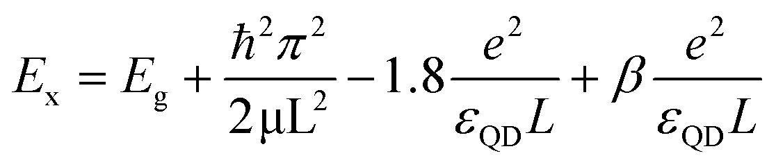
Were, 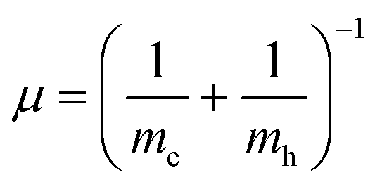 , M = me + mh. Here, me and mh are the effective mass of the electron and hole, respectively and εQD is the dielectric constant of the quantum well. The exciton energy in confined systems is separated into three confinement regimes: weak, strong, and intermediate. In the strong confinement regime, valid when the NC edge length is much smaller than the exciton radius of the material (L ≪ ax), correlation of the electron–hole motion can be neglected, and the exciton energy scales as the inverse square of the NC size (1/L2). For cube-shaped NCs in this regime, the exciton energy is determined by eqn (3).
The opposite limit of the strong confinement regime is the weak confinement when L is much larger than the exciton radius (L ≫ ax). In this weak confinement regime, the electron–hole motion is strongly correlated, and the whole exciton exhibits quantum confinement. Ex is determined in the weak confinement regime in cube-shaped NCs by eqn (4). We note in passing that between these two confinement regimes described above, an “intermediate” confinement regime exists. In order to explain the distinct behavior of the exciton energy between NPLs and nanocubes (eqn (5)) the accepted Brus model40 for QDs confinement was taken into account.
 | (5) |
We approximate β ∼ 0 for the polarization (solvation) term.
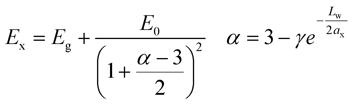
A third model that is presented is an empirical model of Blancon et al.41 for the exciton binding energies of low dimensional systems.42 This model considers both quantum and dielectric confinement effects in a single law-scale formula, with exciton energy described as follow:
 | (6) |
Here, the second term is the exciton ground state binding energy, where E0 (16 meV) and ax (4.6 nm) are the 3D Rydberg energy and Bohr radius of 3D perovskites,43 respectively, and Lw is the quantum well thickness. In this model, the exciton is considered isotropic in α-dimensional space (α strictly greater than 1 and smaller than 3) where γ is an empirical correction factor that accounts for the deviations from the pure quantum confinement regime, including electron and holes densities and dielectric confinement effects. In our case: γEmpirical = 1.76 1 ≤ γ ≤ 3. Other less successful models for NPLs were tested (see Fig. S11†).
The best-fitting model with both automated and manual datasets for exciton energies is the scaling law model (Blancon et al.41) (see Fig. 3b). The decrease in the dimensionality highlights additional compression of the exciton wavefunction in the quantum well due to dielectric confinement, which results in enhanced values of exciton binding energy compared to merely including the quantum confinement effect as for the nanocubes. Blancon et al. in their empirical model explain that the overlap of the electron and hole wavefunctions, whose convolution forms the exciton ground state, becomes more pronounced towards the center of the perovskite layer with increasing thickness.41 This is consistent with the fact that with increasing perovskite layer thickness, the strength of dielectric confinement decreases with respect to quantum confinement.
We thus conclude that the trend of increasing exciton energy with decreasing size for the scaling law model of the NC is less sensitive to dielectric confinement compared to other models and therefore may better explain the discontinuity of exciton energy when transitioning to the NPLs and two-dimensional excitonic regime.
Further support to this conclusion comes from comparison to the study of size-dependent Stokes shift in CsPbBr3 nanocrystals conducted by Brennan et al.27 In their report, they showed that spatial distribution of the hole in CsPbBr3 NCs is delocalized over the entire nanocrystal, and therefore referred to it as confined hole state (CHS). They calculate the electronic structure and hypothesize the existence of a size-dependent CHS from 260 to 70 meV for particles with sizes between ∼2 and 5 nm (measured above the valence band) (Fig. 4a). Similarly, to their representation, we plot the calculated conduction and valence band-edge states (CBES, VBES) from the measured absorption and emission transitions with respect to the CHS, which is set to zero. These calculated energy levels could be used as a reference point in future theoretical work on the exciton dynamics of 1D confined NPLs. For reference, the VBES and CBES values of Brennan et al.27 are also plotted (Fig. 4b).
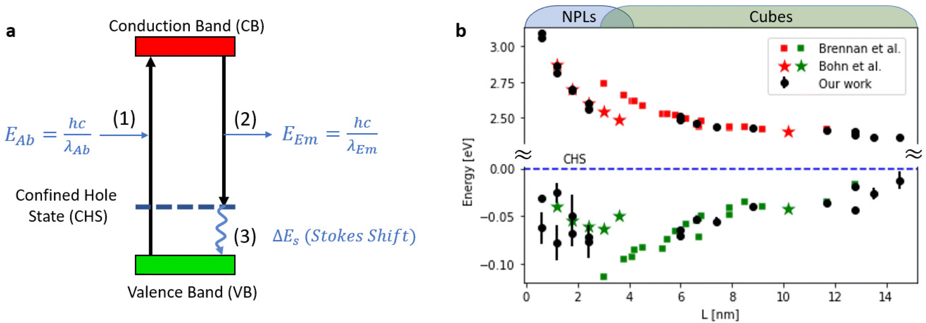 | ||
| Fig. 4 (a) Schematically energetic ordering of relevant absorption and emission transitions within CsPbBr3 NCs (a). Size-dependent NC emission and absorption with theoretical calculation of CBES and VBES energies, plotted relative to CHS energies, which are set to zero (b). | ||
We find agreement between our data for cubic shaped NCs and Brennan's previous work. However, the extension of experiments to NPLs and two-dimensional exciton confinement regime is not trivial. In our measured data the trend becomes non-monotonic and even not continuous. This is clearly shown as a marked decrease in Stokes shift values from 70 to 20 meV for NCs with emission central wavelength of 456 nm (3 ML thickness nanoplates), highlighting the transition from 3D confined excitons to that which is dominated by two-dimensional excitonic dynamics.
When L < 2 nm there is a clear dominance of the NPLs and two-dimensional excitons. Further support to the two-dimensional excitonic behavior for the NPLs regime, is apparent from the agreement to the study of Bohn et al.33 which ultimately focuses on two-dimensional NPLs.
The physical basis to the opposing trends in Stokes shift with size appears to be a more general phenomenon than just 3D and 2D perovskites. In 3D confined quantum dots, smaller sizes lead to larger Stokes Shifts, not only in the CsPbBr3 system discussed here, but also in CsPbI3 and CsPbCl3,28 CdSe,44,45 PbS,46 ZnSe, and InP.47 Conversely, for 1D confined NPLs, the Stokes shifts are generally much smaller than expected48 and may follow no particularly discernible trend with changes in thickness, as in the CdSe nanoplates,49,50 or perhaps even increase with increasing thickness, as shown in this work for CsPbBr3 NPLs and observed elsewhere for (CH3(CH2)3NH3)2(CH3NH3)n−1PbnI3n+1 thin films51 or GaAs quantum dots with variable thickness and the same diameter.52
The cause of this difference between 3D and 2D Stokes shift is not obvious. Conventional approaches suggest that increasing linewidths lead to larger Stokes shifts,53 and for 3D confined systems, the same size dispersion at a smaller size will result in a larger linewidth.54 This leads to increasing Stokes shift with decreasing size. However, single-particle measurements,28 as well as theoretical work, suggest that part or all the increase in Stokes shift may originate from other physical effects. For example, due to changes to the energy level of a dark confined hole state with respect to the valence band edge,27 changes to the exciton fine structure,44 or changes to the electron–hole exchange splitting.45 Considering layered perovskite NPLs, in most syntheses decreasing thickness leads to increasing lateral size,32 a phenomenon that may be explained by equilibria among lead halide precursor nanostructures.30 Conversely, 2D CdSe NPLs do not appear to have this strong inverse correlation between layer thickness and lateral NPL size, which may explain why Stokes shift does not appear to follow any trend for those materials. Given the variability of trends in Stokes shift for 3D/2D confined materials, more experimental studies that follow a data-driven approach of mapping the synthetic landscape are crucial for portraying a more general understanding beyond the examples of 2D perovskites discussed here. For CsPbBr3 nanocrystals, possibilities for future rational synthetic engineering of Stokes shift based on reaction conditions are presented in Fig. S12.† The spread of values marks that no specific single factor which was selected for analysis is responsible for the size-dependent Stokes Shift. Mutual correlation of these factors is needed and will be considered an extension of this work in the future.
The effects studied here are primarily affected by the excitons’ strong/weak confinement regimes in nanoplates/nanocubes, respectively. Thus, we restrict this study to the thicknesses and dimensionality at room temperature. Further temperature dependence spectroscopical studies are in order to understand phonon–exciton interactions. Previous studies on CdSe nanoplates55,56 show that differences in the area of the nanoplates will affect the charge carrier–phonon coupling. This effect is a general physical phenomenon and could also exist in perovskite nanoplates measured under the right conditions. We are confident that such studies and understanding will be complemented in future years.
To conclude, we analyze data from ∼2000 reactions conducted with both automated and manual synthesis spanning a broad synthetic condition landscape. This variety reveals that for CsPbBr3 NPLs with 2D confined excitons, Stokes shift appears to decrease or remain constant. This observation adds to previously reported Stokes shift in nanocubes in which excitons are confined in three dimensions. It is therefore apparent that at these wavelengths, two-dimensional nanoplates with thicknesses nearing a few unit cells, two-dimensional excitons dominate the resulting excitonic dynamics.
Conflicts of interest
The authors declare no competing interests.Acknowledgements
This project has received funding from the European Union's Horizon 2020 research and innovation program under grant agreement no. 949682-ERC-HeteroPlates. The authors would like to thank A.P Alivisatos for his kind advice and guidance. The MIKA staff in the department of materials science and engineering at the Technion, especially Dr Yaron Kauffmann for his continuous support and helpful advice. YB and RS would also like to thank the Russel Berrie Nanotechnology Institute (RBNI) for financial support. Y.B. thanks the Nancy and Stephen Grand Technion Energy Program for generous support. J.C.D. acknowledges support by the National Science Foundation Graduate Research Fellowship under DGE 1752814 and by the Kavli NanoScience Institute, University of California, Berkeley through the Philomathia Graduate Student Fellowship. The automated experimental work at the Molecular Foundry was supported by the Office of Science, Office of Basic Energy Sciences, of the U.S. Department of Energy under Contract No. DE-AC02-05CH11231.References
- X. Peng, et al., Shape control of CdSe nanocrystals, Nature, 2000, 404, 59–61 CrossRef.
- V. I. Klimov, et al., Optical gain and stimulated emission in nanocrystal quantum dots, Science, 2000, 290, 314–317 CrossRef.
- C. B. Murray, C. R. Kagan and M. G. Bawendi, Self-organization of CdSe nanocrystallites into three-dimensional quantum dot superlattices, Science, 1995, 270, 1335–1338 CrossRef.
- L. Manna, E. C. Scher and A. P. Alivisatos, Shape Control of Colloidal Semiconductor Nanocrystals, J. Cluster Sci., 2002, 13, 521 CrossRef.
- Z. Chen, B. Nadal, B. Mahler, H. Aubin and B. Dubertret, Quasi-2D colloidal semiconductor nanoplatelets for narrow electroluminescence, Adv. Funct. Mater., 2014, 24, 295–302 CrossRef.
- C. She, et al., Low-threshold stimulated emission using colloidal quantum wells, Nano Lett., 2014, 14, 2772–2777 CrossRef.
- M. Olutas, et al., Lateral size-dependent spontaneous and stimulated emission properties in colloidal CdSe nanoplatelets, ACS Nano, 2015, 9, 5041–5050 CrossRef PubMed.
- C. She, et al., Red, Yellow, Green, and Blue Amplified Spontaneous Emission and Lasing Using Colloidal CdSe Nanoplatelets, ACS Nano, 2015, 9, 9475–9485 CrossRef PubMed.
- L. Li and P. Reiss, One-pot synthesis of highly luminescent InP/ZnS nanocrystals without precursor injection, J. Am. Chem. Soc., 2008, 130, 11588–11589 CrossRef.
- J. Ziegler, et al., Silica-Coated InP/ZnS Nanocrystals as Converter Material in White LEDs, Adv. Mater., 2008, 20, 4068–4073 CrossRef CAS.
- L. Protesescu, et al., Nanocrystals of cesium lead halide perovskites (CsPbX3, X = Cl, Br, and I): novel optoelectronic materials showing bright emission with wide color gamut, Nano Lett., 2015, 15, 3692–3696 CrossRef CAS PubMed.
- D. Yang, et al., All-inorganic cesium lead halide perovskite nanocrystals: synthesis, surface engineering and applications, J. Mater. Chem. C, 2019, 7, 757–789 RSC.
- M. V. Kovalenko, L. Protesescu and M. I. Bodnarchuk, Properties and potential optoelectronic applications of lead halide perovskite nanocrystals, Science, 2017, 358, 745–750 CrossRef CAS.
- Y. Chen, X. Liu, T. Wang and Y. Zhao, Highly Stable Inorganic Lead Halide Perovskite toward Efficient Photovoltaics, J. Am. Chem. Soc., 2021, 54, 3452–3461 CAS.
- H. J. Snaith, Perovskites: The Emergence of a New Era for Low-Cost, High-Efficiency Solar Cells, J. Phys. Chem. Lett., 2013, 4, 3623–3630 CrossRef CAS.
- C.-Y. Huang, et al., CsPbBr3 Perovskite Quantum Dot Vertical Cavity Lasers with Low Threshold and High Stability, ACS Photonics, 2017, 4, 2281–2289 CrossRef.
- Dryad Data – High-throughput Synthesis and Transformations of CsPbBr nanocrystals characterized by UV-Vis Absorption and Fluorescence. https://datadryad.org/stash/dataset/doi%253A10.6078%252FD1XT4F.
- L. Lang, J. H. Yang, H. R. Liu, H. J. Xiang and X. G. Gong, First-principles study on the electronic and optical properties of cubic ABX3 halide perovskites, Phys. Lett. A, 2014, 378, 290–293 CrossRef.
- S. ten Brinck and I. Infante, Surface Termination, Morphology, and Bright Photoluminescence of Cesium Lead Halide Perovskite Nanocrystals, ACS Energy Lett., 2016, 1, 1266–1272 CrossRef.
- J. Kang and L.-W. Wang, High Defect Tolerance in Lead Halide Perovskite CsPbBr3, J. Phys. Chem. Lett., 2017, 8, 489–493 CrossRef PubMed.
- C. Yang and R. Lunt, Limits of visibly transparent luminescent solar concentrators, Adv. Opt. Mater., 2017, 5, 1600851 CrossRef.
- N. D. Bronstein, et al., Quantum Dot Luminescent Concentrator Cavity Exhibiting 30-fold Concentration, ACS Photonics, 2015, 2, 1576–1583 CrossRef CAS.
- E. Yablonovitch, Thermodynamics of the fluorescent planar concentrator, J. Opt. Soc. Am., 1980, 70, 1362–1363 CrossRef.
- Z. Gan, W. Chen, L. Yuan, G. Cao and C. Zhou, External stokes shift of perovskite nanocrystals enlarged by photon recycling External stokes shift of perovskite nanocrystals enlarged by photon recycling, Appl. Phys. Lett., 2019, 114, 011906 CrossRef.
- A. L. Efros, et al., Band-edge exciton in quantum dots of semiconductors with a degenerate valence band: Dark and bright exciton states, Phys. Rev. B, 1996, 54, 4843–4856 CrossRef CAS PubMed.
- M. C. Brennan, J. Zinna and M. Kuno, Existence of a Size-Dependent Stokes Shift in CsPbBr3 Perovskite Nanocrystals, ACS Energy Lett., 2017, 2, 1487–1488 CrossRef CAS.
- M. C. Brennan, et al., Origin of the Size-Dependent Stokes Shift in CsPbBr3 Perovskite Nanocrystals, J. Am. Chem. Soc., 2017, 139, 12201–12208 CrossRef CAS PubMed.
- M. C. Brennan, et al., Universal Size-Dependent Stokes Shifts in Lead Halide Perovskite Nanocrystals, J. Phys. Chem. Lett., 2020, 11, 4937–4944 CrossRef.
- S. Toso, D. Baranov and L. Manna, Metamorphoses of Cesium Lead Halide Nanocrystals, Acc. Chem. Res., 2021, 54, 498–508 CrossRef PubMed.
- J. C. Dahl, X. Wang, X. Huang, E. M. Chan and A. P. Alivisatos, Elucidating the Weakly Reversible Cs–Pb–Br Perovskite Nanocrystal Reaction Network with High-Throughput Maps and Transformations, J. Am. Chem. Soc., 2020, 142, 11915–11926 CrossRef PubMed.
- M. Imran, et al., Benzoyl halides as alternative precursors for the colloidal synthesis of lead-based halide perovskite nanocrystals, J. Am. Chem. Soc., 2018, 140, 2656–2664 CrossRef PubMed.
- Y. Bekenstein, B. A. Koscher, S. W. Eaton, P. Yang and A. P. Alivisatos, Highly Luminescent Colloidal Nanoplates of Perovskite Cesium Lead Halide and Their Oriented Assemblies, J. Am. Chem. Soc., 2015, 137, 16008–16011 CrossRef CAS PubMed.
- B. J. Bohn, et al., Boosting Tunable Blue Luminescence of Halide Perovskite Nanoplatelets through Postsynthetic Surface Trap Repair, Nano Lett., 2018, 18, 5231–5238 CrossRef CAS PubMed.
- J. De Roo, et al., Highly Dynamic Ligand Binding and Light Absorption Coefficient of Cesium Lead Bromide Perovskite Nanocrystals, ACS Nano, 2016, 10, 2071–2081 CrossRef PubMed.
- J. A. Sichert, et al., Quantum Size Effect in Organometal Halide Perovskite Nanoplatelets, Nano Lett., 2015, 15, 6521–6527 CrossRef PubMed.
- D. L. Ferreira, et al., Size-dependent bandgap and particle size distribution of colloidal semiconductor nanocrystals, J. Chem. Phys., 2017, 147, 154102 CrossRef PubMed.
- C. C. Wu and P. H. Roberts, Shock-wave propagation in a sonoluminescing gas bubble, Phys. Rev. Lett., 1993, 70, 3424 CrossRef PubMed.
- A. I. Ekimov, A. L. Efros and A. A. Onushchenko, Quantum size effect in semiconductor microcrystals, Solid State Commun., 1985, 56, 921–924 CrossRef CAS.
- A. Efros, Interband Light Absorption in Semiconductor Spheres, Sov. Phys. Semicond., 1982, 16, 1209–1214 CAS.
- L. E. Brus, Electron – electron and electron-hole interactions in small semiconductor crystallites: The size dependence of the lowest excited electronic state, J. Chem. Phys., 1984, 80, 4403 CrossRef CAS.
- J. Blancon, et al., Scaling law for excitons in 2D perovskite quantum wells, Nat. Commun., 2018, 9, 1–10 CrossRef CAS.
- P. Christol, P. Lefebvre and H. Mathieu, Fractional–dimensional calculation of exciton binding energies in semiconductor quantum wells and quantum–well wires, J. Appl. Physics, 1993, 74, 5626–5637 CrossRef CAS.
- A. Miyata, et al., Direct measurement of the exciton binding energy and effective masses for charge carriers in organic–inorganic tri-halide perovskites, Nat. Phys., 2015, 11, 582–587 Search PubMed.
- M. Kuno, J. K. Lee, B. O. Dabbousi, F. V. Mikulec and M. G. Bawendi, The band edge luminescence of surface modified CdSe nanocrystallites: Probing the luminescing state, J. Chem. Phys., 1997, 106, 9869–9882 CrossRef CAS.
- D. O. Demchenko and L. W. Wang, Optical transitions and nature of Stokes shift in spherical CdS quantum dots, Phys. Rev. B: Condens. Matter Mater. Phys., 2006, 73, 155326 CrossRef.
- P. B. Green, Z. Li and M. W. B. Wilson, PbS Nanocrystals Made with Excess PbCl2 Have an Intrinsic Shell that Reduces Their Stokes Shift, J. Phys. Chem. Lett., 2019, 10, 5897–5901 CrossRef CAS PubMed.
- O. I. Mićić, et al., Size-dependent spectroscopy of InP quantum dots, J. Phys. Chem. B, 1997, 101, 4904–4912 CrossRef.
- S. Ithurria, G. Bousquet and B. Dubertret, Continuous transition from 3D to 1D confinement observed during the formation of CdSe nanoplatelets, J. Am. Chem. Soc., 2011, 133, 3070–3077 CrossRef CAS PubMed.
- S. Ithurria and D. V. Talapin, Colloidal Atomic Layer Deposition (c-ALD) using self-limiting reactions at nanocrystal surface coupled to phase transfer between polar and nonpolar media, J. Am. Chem. Soc., 2012, 134, 18585–18590 CrossRef CAS PubMed.
- S. Christodoulou, et al., Chloride-Induced Thickness Control in CdSe Nanoplatelets, Nano Lett., 2018, 18, 6248–6254 CrossRef CAS.
- J. Cao, et al., Alkali-cation-enhanced benzylammonium passivation for efficient and stable perovskite solar cells fabricated through sequential deposition, J. Mater. Chem. A, 2020, 8, 19357–19366 RSC.
- N. Ha, et al., Size-dependent line broadening in the emission spectra of single GaAs quantum dots: Impact of surface charge on spectral diffusion, Phys. Rev. B: Condens. Matter Mater. Phys., 2015, 92, 075306 CrossRef.
- F. Yang, M. Wilkinson, E. J. Austin and K. P. O'Donnell, Origin of the Stokes shift: A geometrical model of exciton spectra in 2D semiconductors, Phys. Rev. Lett., 1993, 70, 323 CrossRef CAS PubMed.
- J. Sun and E. M. Goldys, Linear Absorption and Molar Extinction Coefficients in Direct Semiconductor Quantum Dots, J. Phys. Chem. C, 2008, 112, 9261–9266 CrossRef CAS.
- R. Scott, et al., A comparative study demonstrates strong size tunability of carrier-phonon coupling in CdSe-based 2D and 0D nanocrystals, Nanoscale, 2019, 11, 3958 RSC.
- A. W. Achtstein, et al., Tuning exciton diffusion, mobility and emission line width in CdSe nanoplatelets via lateral size, Nanoscale, 2020, 12, 23521 RSC.
Footnote |
| † Electronic supplementary information (ESI) available: Additional data analysis, Stokes shifts vs. wavelength. Statistical error calculation for the Stokes shift, estimation of NCs sizes from spectra, additional theoretical models for cubes and plates. See DOI: https://doi.org/10.1039/d2nr03275a |
| This journal is © The Royal Society of Chemistry 2022 |