
 Open Access Article
 This Open Access Article is licensed under a
 Creative Commons Attribution 3.0 Unported Licence
Large piezoelectric response in ferroelectric/multiferroelectric metal oxyhalide MOX2 (M = Ti, V and X = F, Cl and Br) monolayers†
Mohammad
Noor-A-Alam
 * and
Michael
Nolan
*
* and
Michael
Nolan
*
Tyndall National Institute, Lee Maltings, Dyke Parade, University College Cork, T12R5CP Cork, Ireland. E-mail: mda.alam@tyndall.ie; michael.nolan@tyndall.ie
First published on 11th July 2022
Abstract
Flexible two-dimensional (2D) piezoelectric materials are promising for applications in wearable electromechanical nano-devices such as sensors, energy harvesters, and actuators. A large piezo-response is required for any practical applications. Based on first-principles calculations, we report that ferroelectric TiOX2 and multiferroelectric VOX2 (X = F, Cl, and Br) monolayers exhibit large in-plane stress (e11) and strain (d11) piezoelectric coefficients. For example, the in-plane piezo-response of TiOBr2 (both e11 = 28.793 × 10⁻¹⁰ C m−1 and d11 = 37.758 pm V−1) is about an order of magnitude larger than that of the widely studied 1H-MoS2 monolayer, and also quite comparable to the giant piezoelectricity of group-IV monochalcogenide monolayers, e.g., SnS. Moreover, the d11 of MOX2 monolayers – ranging from 29.028 pm V−1 to 37.758 pm V−1 – are significantly higher than the d11 or d33 of commonly used 3D piezoelectrics such as w-AlN (d33 = 5.1 pm V−1) and α-quartz (d11 = 2.3 pm V−1). Such a large d11 of MOX2 monolayers originates from low in-plane elastic constants with large e11 due to large Born effective charges (Zij) and atomic sensitivity  to an applied strain. Moreover, we show the possibility of opening a new way of controlling piezoelectricity by applying a magnetic field.
1 Introduction
Insulators or semiconductors that lack inversion symmetry exhibit a piezoelectric effect, which is an electromechanical coupling that allows energy conversion from mechanical to electrical, and vice versa. This effect is used in many important applications such actuators, sensors, and transducers.1,2 Current trends in the miniaturization of devices require piezoelectricity at the nanoscale. Being at most a few atomic-layers thick, 2D piezoelectrics have potential for miniaturizing these electromechanical devices down to nanoscale. Moreover, compared with 3D piezoelectrics (e.g., bulk crystals or thin-films), few layered (typically 1–3 layers) piezoelectric materials can generally exhibit larger deformation.1,2 Importantly, nowadays these 2D materials can be grown with good crystalline quality. Hence, 2D piezoelectrics become promising for self-powered, flexible, and wearable nano-devices. These 2D piezoelectrics can also find interesting applications in new types of electronics such as piezotronics1 – where the electronic band gap is controlled by the electric potential stemming from piezoelectricity – and in piezo-photonics,2 where light is coupled with the piezoelectrically induced charges. For example, it has been predicted that the performance of MoS2-based solar cells can be enhanced by the coupling of semiconducting and piezoelectric properties.3Quite often, reduction in materials dimension promotes unique properties. For example, bulk 2H-MoS2 is a non-piezoelectric due to its centrosymmetry, whereas the monolayer (also odd numbered layers e.g., trilayer) has no inversion symmetry – and exhibits piezoelectric properties.4 In agreement with the theory,4 in-plane piezoelectricity in a 1H-MoS2 monolayer, which is comparable to the piezo-response of commercially used wurtzite nitrides, e.g., the d33 of w-AlN (5.1 pm V−1), has been confirmed by recent experiments.5 However, generally speaking, a high piezo-response in these 2D materials is desired for any device-level applications. Therefore, enhancement of piezoelectricity and discovery of new 2D piezoelectrics have drawn significant research interest. Typically, 1H-type (D3h symmetry)6–9 (e.g., d11 = 13.45 pm V−1 for 1H-CrTe2)6 and Janus 1T-type10–12 (e.g., d22 = 4.12 pm V−1 for 1T-MoSSe)10 2D materials have been investigated for a large piezoelectric response. So far, piezoelectricity has been predicted in several families of non-ferroelectric 2D materials, like doped or chemically modified graphene,13–15 metal dichalcogenides or oxides, and Janus monolayers.6–9,11,16–18 Encouragingly, although 2D ferroelectrics are relatively rare to date, giant in-plane piezoelectric response is present in the ferroelectric monolayers of group-IV monochalcogenides19 and MXenes (e.g., Sc2CS2).20 A huge out-of-plane piezo-response (d33 = 172.61 pm V−1) is observed in buckled monolayers.21 Ferroelectric In3Se3 nanoflakes22 also show a moderate out-of-plane piezo-response. Furthermore, the co-existence of piezoelectricity and magnetism and their coupling in 2D materials – namely vanadium dichalcogenide monolayers,23 Janus ferromagnetic NiClI monolayers,11 and 1H-LaBr2 monolayers24– have been investigated. Any strong coupling between piezoelectricity and magnetism can be utilized for making piezoelectric-based multifunctional nano-devices. In this regard, multiferroelectric materials are interesting because they usually exhibit good coupling between electric polarization and magnetic order. Piezoelectricity is linked with electric polarization – for instance, the piezoelectric stress co-efficient (eij) is defined as  where strain ∂ηj along the j-direction induces polarization along the i-direction (∂Pi). However, how changes in the magnetic order will change the piezo-response in 2D multiferroelectrics – where polarization couples with the magnetic order – remains unanswered to the best of our knowledge.
Based on first-principles calculations, several approaches such as defect engineering,25 doping/charging,26 and chemical functionalization27,28 have been proposed for combining ferroelectricity and magnetism in 2D materials. There are also a limited number of intrinsically multiferroelectric 2D materials discovered recently – including the metal phosphorus chalcogenides family,29,30 buckled CrN and CrB2 monolayers,31 and MXene Hf2VC2F2 monolayers.32 Multiferroelectricity in the monolayers of the metal oxyhalide VOX2 family33–37 has been predicted with interesting violation of the d0 rule.38 In VOX2 monolayers, the ferroelectric polarization direction is perpendicular to the partially occupied dxy orbital that is the origin of magnetism. As a result, the partially occupied d orbital does not suppress the ferroelectric atomic displacement. Moreover, compared to ferroelectric TiOX2 monolayers with the empty d orbital, the presence of an electron in the dxy of VOX2 monolayers rather positively contributes to the total electric polarization.34 Initially, the ground state of the VOI2 monolayer was predicted as ferromagnetic and ferroelectric.34 However, later it has been predicted that the ferroelectric VOI2 monolayer can exhibit spiral magnetism for a short period due to iodine's strong (compared to other halogens) spin–orbit coupling (SOC).36,37 Alternatively, ferroelectricity in the VOI2 monolayer can also be suppressed by on-site strong Coulomb interaction making it a ferromagnetic metal.37 The coexistence of ferroelectricity and ferromagnetism is predicted in the VOF2 monolayer,35 whereas VOCl2 and VOBr2 monolayers have a ferroelectric ground state with antiferromagnetic (AFM) spin order.33,34 Note that the VOCl2 monolayer can be exfoliated experimentally from its bulk layered van der Waals structure (space group: Immm).33 Generally, ferroelectric materials exhibit good piezoelectricity. Although ferroelectricity and multiferroelectricity of MOX2 monolayers have been investigated,33–37 their piezoelectric properties remain unknown to date. In this paper, we investigate the piezoelectric properties of both TiOX2 and VOX2 monolayers and how the piezo-response changes with magnetic order, which remain unexplored to date. We find that these monolayers exhibit a remarkably large piezo-response compared to most of the known 2D piezoelectrics, and they are promising materials for nanoscale electromechanical applications.
2 Computational details
Our first-principles calculations are performed in the framework of spin-polarized density functional theory as implemented in the Vienna Ab initio Simulation Package (VASP) based on a plane-wave basis set.39 The projector augmented wave (PAW) potentials40 are used for describing the core electrons. The generalized gradient approximation (GGA) of Perdew, Burke, and Ernzernhof (PBE)41 is employed for treating the exchange and correlation. The valence electron configurations considered for Ti, V, O, F, Cl, and Br are 3d3 4s1 (4 electrons), 3d4 4s1 (5 electrons), 2s2 2p4 (6 electrons), 2s2 2p5 (7 electrons), 3s2 3p5 (7 electrons), and 4s2 4p5 (7 electrons), respectively. A cutoff energy of 500 eV is used for the plane-wave expansion in all calculations. All structures are fully relaxed until the Hellmann–Feynman forces on all the atoms are less than 10−3 eV Å−1. The lattice parameters a and b are relaxed, keeping c fixed as required for 2D materials, and the internal coordinates of the 2D structures are fully relaxed to achieve the lowest energy configuration using the conjugate gradient algorithm. To prevent the interaction between the periodic images in the calculations, a vacuum layer with a thickness of approximately 25 Å is added along the z-direction (perpendicular to the monolayer) in the supercell. Note that previous reports33–35 employed about 15–20 Å vacuum layers, and also considered the van der Waals interaction between the layers.33,35 However, we have not considered the van der Waals interaction as we simulate an isolated monolayer. The convergence for the total energy is set as 10−7 eV. For a 1 × 1 × 1 unit cell, the Brillouin zone integration is sampled using a regular 12 × 12 × 1 Monkhorst–Pack k-point grid for geometry optimizations, while a denser grid of 18 × 18 × 1 is used for density functional perturbation theory (DFPT) calculations. To study magnetic ordering, 1 × 2 × 1, 2 × 1 × 1, and 2 × 2 × 1 VOX2 supercells (shown in Fig. 1(c)) with 12 × 6 × 1, 6 × 12 × 1, and 6 × 6 × 1 Monkhorst–Pack k-point grids, respectively are used. The elastic stiffness coefficients (Cij) are obtained using a finite difference method as implemented in the VASP code. DFPT is used to calculate the Born effective charges (Zij) and ionic and electronic parts of piezoelectric (eij) tensors. A 4 × 4 × 1 supercell is used for the phonon dispersion calculations of the monolayers, which is obtained with PHONOPY code42 using the DFPT method. Recently it has been found that the Hubbard effective U (Ueff) correction does not alter the magnetic and ferroelectric properties of VOF2.35 However, to confirm the lack of impact of the Hubbard + U correction on the piezoelectric response of VOBr2, we apply the GGA + Ueff (Ueff ranging from 1 eV to 3 eV) approach43 for the 3d orbitals of V. We find that the Hubbard Ueff correction increases both e11 and d11 (see the ESI†). This further supports our conclusion that VOBr2 has a large piezoelectric response.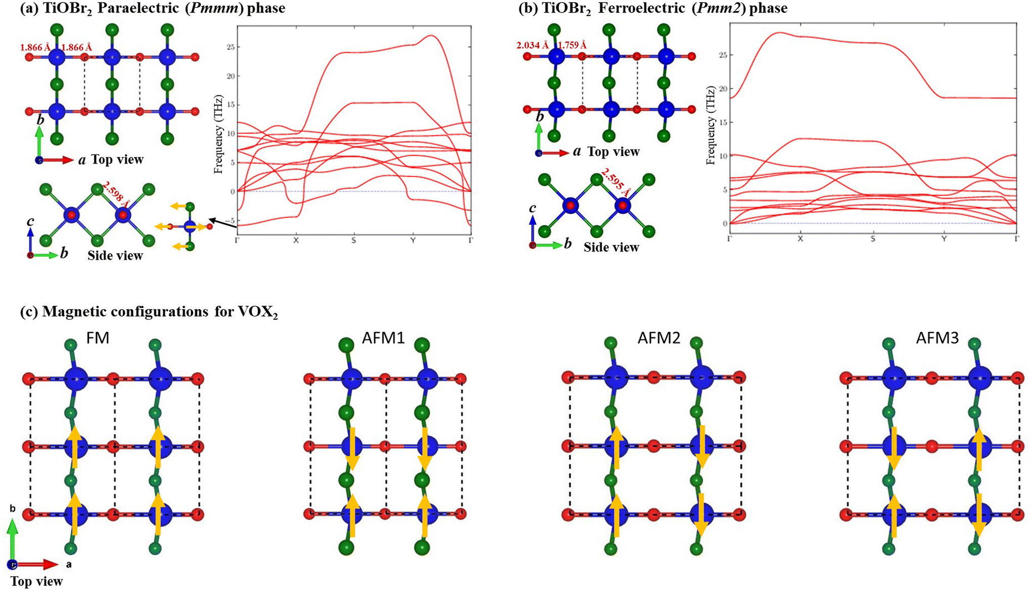 | ||
| Fig. 1 As a representative of MOX2 monolayers, top and side views of the TiOBr2 monolayer in (a) the paraelectric and (b) ferroelectric phases are shown. Beside the structure, the phonon band structure is also shown. We see an imaginary phonon (soft) mode at the Γ-point for paraelectric TiOBr2; the vibration mode is indicated by the black arrow, whereas yellow arrows represent the direction of atomic displacement associated with the imaginary mode. In the phonon band structure, Γ(0,0,0), X(1/2,0,0), S(1/2,1/2,0), and Y(0,1/2,0) are the high symmetric points in the Brillouin zone. Blue, red, and green balls represent Ti/V, O, and F/Cl/Br, respectively. (c) The four magnetic configurations for VOX2 monolayers are shown; yellow arrows represent the collinear spin direction (up or down). The dashed lines represent the rectangle simulation cells. | ||
3 Results and discussion
We start with the fully optimized centrosymmetric paraelectric (and also ferromagnetic for VOX2) phase (space group: Pmmm) of MOX2 monolayers and calculated their phonon dispersion. We find that there is an imaginary (soft) optical vibration mode at the center of the Brillouin zone (Γ-point) for the PE phase (see Fig. 1(a) for TiOBr2 and also the ESI† for other MOX2 monolayers). The frequency (iωΓ) associated with the polar soft mode is given in Table 1. This suggests that there is a spontaneous atomic displacement of Ti(V) along the Ti–O (V–O) chain, breaking the inversion symmetry, thus producing a spontaneous in-plane (along the a-direction) electric polarization. This can also be understood in terms of long and short Ti–O (V–O) bonds along the a-direction in the FE phase (space group: Pmm2), whereas all M–O bonds are the same in the PE phase. Therefore, the a lattice parameter of the FE phase becomes slightly larger than that of the PE phase, although the b lattice parameter remains almost unchanged (see Table 1). As Ti4+ and V4+ have almost the same ionic radii, their lattice parameters are close. We see an increase in b as the radius of X increases from F to Br, which is expected because X atoms are only along the b-direction. With the exception of TiOF2 (FE), the phonon dispersion of FE MOX2 monolayers shows no appreciable soft mode, indicating their stability. Interestingly, we find that the ground state of the TiOF2 monolayer is not the FE (Pmm2) phase – rather the non-polar (Pmma) phase (see the ESI†), which is 26.620 meV per atom lower in energy than the FE phase – therefore, we will not discuss its properties in the main paper.| a (Å) | b (Å) | M–O (Å) | M–X (Å) | Z 11 (M) | Z 11 (O) | Z 11 (X) | P 1 (10−12 C m−1) | ΔE (meV per fu) | iω Γ (cm−1) | |
|---|---|---|---|---|---|---|---|---|---|---|
| VOF2(FM) | 3.765(3.600) | 3.025(3.055) | 1.649(1.800) | 1.969(1.971) | 5.458(13.235) | −4.142 (−10.188) | −0.659 (−1.415) | 309.192 | 124.809 | 385.919 |
| VOCl2(FM) | 3.773(3.610) | 3.454(3.480) | 1.653(1.805) | 2.388(2.397) | 4.893(14.703) | −4.255 (−12.174) | −0.319 (−1.197) | 288.284 | 119.122 | 351.430 |
| VOCl2(AFM1) | 3.784(3.609) | 3.367(3.408) | 1.650(1.804) | 2.383(2.395) | 4.825(15.171) | −4.186 (−12.926) | −0.319 (−1.122) | 311.609 | 129.095 | 396.542 |
| VOBr2(FM) | 3.764(3.620) | 3.649(3.620) | 1.664(1.810) | 2.545(2.557) | 5.018(15.076) | −4.579 (−12.965) | −0.219 (−1.029) | 254.575 | 82.916 | 285.802 |
| VOBr2(AFM1) | 3.769(3.619) | 3.577(3.615) | 1.661(1.810) | 2.542(2.555) | 5.025(14.931) | −4.580 (−13.065) | −0.222 (−0.933) | 271.205 | 85.646 | 301.611 |
| TiOCl2 | 3.793(3.719) | 3.504(3.518) | 1.745(1.859) | 2.438(2.441) | 7.506(12.291) | −6.723 (−11.011) | −0.391 (−0.391) | 185.430 | 26.519 | 227.851 |
| TiOBr2 | 3.792(3.732) | 3.677(3.689) | 1.759(1.866) | 2.595(2.598) | 7.931(11.973) | −7.347 (−11.012) | −0.289 (−0.480) | 160.291 | 16.254 | 170.826 |
As electric polarization (P1) arises due to the polar distortion from the PE phase, we calculated P1 in the 2D unit (C m−1) using Z11 and the atomic displacement (Δuk,1) of the k-th atom along the a-direction as 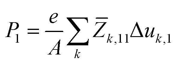 . The sum runs over all the atoms in the simulation cell; A is the area of the cell and e is charge of an electron. We use mean BECs (
![[Z with combining macron]](https://www.rsc.org/images/entities/i_char_005a_0304.gif) k,11) – i.e.,
k,11) – i.e.,  because Z11 changes during the PE-to-FE phase transition. For the PE phase, we find anomalously large Z11, which decreases after the PE-to-FE transition (see Table 1). Similar anomalous BECs have been observed for other well-known ferroelectric materials.44 In agreement with previous reports,35 we find that MOX2 monolayers have quite large P1, which is comparable with that of group-IV monochalcogenide orthorhombic monolayers, e.g., SnS (P1 = 2.47 × 10⁻¹⁰ C m−1).45,46 We also estimated the energy barrier for FE polarization switching. We take the difference in energy (ΔE) between FE and PE phases; lattice parameters a and b are fully relaxed in both phases. Our ΔE values are in good agreement with the reported values. We see a general trend that P1, ΔE, and iωΓ decrease as the ionic radius of X increases from F to Br. Interestingly, we also observed that magnetic VOX2 monolayers have significantly larger P1 than non-magnetic TiOCl2 or TiOBr2. This is in line with the previous report that the presence of an electron in the dxy orbital of V does not suppress but rather enhances ferroelectric polarization.34 This is also confirmed by the larger iωΓ of VOX2 (see Table 1).
To examine the impact of magnetic configuration on VOX2 monolayers, we consider four (1 FM and 3 AFM) collinear magnetic spin configurations (see Fig. 1(c) and Table 2). Each V4+ contributes 1μB, which comes from an unpaired electron in the dxy orbital.34 Comparing the energy difference of an AFM configuration with respect to the FM order, in agreement with previous reports, we find that the FE VOF2 monolayer has an FM ground state.35 However, we find that the AFM3-type AFM order (see Fig. 1(c)) is more stable than other configurations in VOCl2 and VOBr2 monolayers.33,34 The alternating up and down collinear spin configuration of V atoms along the b-direction (see Fig. 1(c)) shortens the b lattice parameter, compared with that of the FM state (shown in Table 1). By applying an external magnetic field in an experiment, the AFM order can be changed to FM. This will also lead a change in P1 with a reduction of 7.49% and 6.13% for AFM1-to-FM transition in VOCl2 and VOBr2 monolayers, respectively. The AFM1-to-FM transition slightly hardens the soft mode (iωΓ; see Table 1; also see the ESI† for AFM3), and consequently reduces the ferroelectric switching barrier (ΔE) slightly. This indicates that there is a weak coupling between the magnetic and ferroelectric orders in VOX2.
| ΔEAFM1 | ΔEAFM2 | ΔEAFM3 | |
|---|---|---|---|
| VOF2 | 9.183 | 2.170 | 9.789 |
| VOCl2 | −20.331 | 3.652 | −22.019 |
| VOBr2 | −9.437 | 4.774 | −11.257 |
All ferroelectrics exhibit piezoelectricity. It is interesting to know the piezo-response of our FE MOX2 monolayers as strong in-plane piezoelectricity has already been predicted in 2D FE group-IV monochalcogenides.19 Our calculated piezoelectric stress coefficients (eij) are shown in Table 3. eij are important coefficients for estimating the figure-of-merit of a piezoelectric thin-film (TFFOM); usually the larger the eij, the higher the figure-of-merit. Because strain along the z-direction (vacuum) is ill-defined in 2D materials, we have only three independent piezoelectric coefficients: e11, e12, and e16. There is a mirror symmetry along the b-direction, which does not allow any polarization in that direction, thus e22 = 0. However, strain along the b-direction can induce polarization along the a-direction, which results in a non-zero e12 coefficient. The FE MOX2 monolayer (space group: Pmm2) due to the mm2 point group has a symmetry of reflection with reference to the M–O atomic plane. This prohibits an out-of-plane electric polarization, thus e31 = 0. We mainly focus on the piezo-response related to uniaxial strain along the a-direction (η1) and the b-direction (η2), which are e11(d11) and e12(d12), respectively. e16 is associated with shear strain (η12),19 and we exclude it for simplicity.
 or
or  represents the change of the atomic coordinates along the a-direction in response to a strain along the a-direction (η1) or the b-direction (η2), respectively
| e elc11 | e ion11 | e 11 |
|
|
|
e elc12 | e ion12 | e 12 |
|
|
|
|
|---|---|---|---|---|---|---|---|---|---|---|---|---|
| VOF2(FM) | 5.776 | 13.850 | 19.625 | 0.271 | −0.242 | −0.015 | 4.513 | −0.867 | 3.646 | −0.073 | −0.060 | 0.066 |
| VOCl2(FM) | 4.524 | 11.397 | 15.921 | 0.315 | −0.213 | −0.051 | 3.354 | −0.639 | 2.716 | −0.044 | −0.037 | 0.041 |
| VOCl2(AFM1) | 4.693 | 11.407 | 16.100 | 0.314 | −0.209 | −0.052 | 3.309 | −0.693 | 2.616 | −0.029 | −0.021 | 0.025 |
| VOBr2(FM) | 4.217 | 11.937 | 16.153 | 0.371 | −0.195 | −0.088 | 2.974 | −0.824 | 2.150 | −0.039 | −0.031 | 0.035 |
| VOBr2(AFM1) | 4.331 | 12.384 | 16.715 | 0.371 | −0.191 | −0.090 | 2.962 | −0.437 | 2.526 | −0.029 | −0.022 | 0.025 |
| TiOCl2 | 3.764 | 22.345 | 26.109 | 0.494 | −0.177 | −0.159 | 1.819 | −1.103 | 0.716 | −0.038 | −0.028 | 0.033 |
| TiOBr2 | 3.250 | 25.543 | 28.793 | 0.599 | −0.162 | −0.218 | 1.531 | −0.737 | 0.794 | −0.034 | −0.024 | 0.029 |


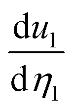
Table 3 shows that the TiOCl2 or TiOBr2 monolayer has quite large e11 but small e12, compared to those of VOX2 monolayers. We also notice that unlike 1H-type monolayers, e.g., 1H-MoS2 where e11 = −e12 due to the ![[6 with combining macron]](https://www.rsc.org/images/entities/char_0036_0304.gif) m2 point group symmetry, MOX2 monolayers exhibit a highly anisotropic piezo-response, where e11 is significantly larger than e12. This is also expected as the monolayers have a strong in-plane electric polarization P1, hence atomic displacement in response to strain along the a-direction can change P1 directly. Interestingly, we observe a general trend that the in-plane piezo-response (e11) decreases as the in-plane polarization increases (see Tables 1 and 3). To understand the origin of the large/small piezoelectric constant, we split e11 and e12 into two terms – (i) the clamped-ion term (eelc11 or eelc12), which is the electronic contribution where the atoms are fixed at their equilibrium internal coordinates (u) and (ii) the ionic contribution term (eion11 or eion12), due to the atomic displacements in response to a macroscopic strain η1 (η2) along the a-direction (b-direction). The eion11 of TiOCl2 and TiOBr2 monolayers is almost twice larger than that of VOX2. Interestingly, we notice that both ionic and electronic parts of e11 are positive (see Table 3), thus they contribute positively to the total e11 – similar to 1H-MoS2.24 That is why the TiOCl2 or TiOBr2 monolayer has significantly large e11, compared to that of VOX2, although the eelc11 of TiOCl2 and TiOBr2 monolayers is slightly smaller than that of VOX2. On the other hand, the ionic and electronic parts of e12 are opposite in sign, hence they reduce the total e12. We see that because of their small positive eelc12 but large negative eion12, TiOCl2 and TiOBr2 monolayers have quite small e12 (see Table 3). We further split the ionic part:24,47,48
m2 point group symmetry, MOX2 monolayers exhibit a highly anisotropic piezo-response, where e11 is significantly larger than e12. This is also expected as the monolayers have a strong in-plane electric polarization P1, hence atomic displacement in response to strain along the a-direction can change P1 directly. Interestingly, we observe a general trend that the in-plane piezo-response (e11) decreases as the in-plane polarization increases (see Tables 1 and 3). To understand the origin of the large/small piezoelectric constant, we split e11 and e12 into two terms – (i) the clamped-ion term (eelc11 or eelc12), which is the electronic contribution where the atoms are fixed at their equilibrium internal coordinates (u) and (ii) the ionic contribution term (eion11 or eion12), due to the atomic displacements in response to a macroscopic strain η1 (η2) along the a-direction (b-direction). The eion11 of TiOCl2 and TiOBr2 monolayers is almost twice larger than that of VOX2. Interestingly, we notice that both ionic and electronic parts of e11 are positive (see Table 3), thus they contribute positively to the total e11 – similar to 1H-MoS2.24 That is why the TiOCl2 or TiOBr2 monolayer has significantly large e11, compared to that of VOX2, although the eelc11 of TiOCl2 and TiOBr2 monolayers is slightly smaller than that of VOX2. On the other hand, the ionic and electronic parts of e12 are opposite in sign, hence they reduce the total e12. We see that because of their small positive eelc12 but large negative eion12, TiOCl2 and TiOBr2 monolayers have quite small e12 (see Table 3). We further split the ionic part:24,47,48
 | (1) |
 | (2) |
 . Similarly,
  represents the change in the k-th atom's internal coordinate along the a-direction (u1(k)) in response to a macroscopic strain (η2) along the b-direction. Relaxing the atomic positions in response to the strains η1 and η2, we obtain the slopes
  and
and  , respectively. We notice that the large eion11 of TiOCl2 and TiOBr2 monolayers comes from their large Z11 (see Table 1) and
  (see Table 3). Also, we see that the
  of Ti/V/O is an order of magnitude larger than
  – i.e., the uniaxial strain η1 can displace atoms along the a-direction more than η2. This also gives the large difference between eion11 and eion12. Moreover, we observe that the AFM1 order of VOCl2 and VOBr2 marginally enhances e11 because of a slight increase in both eelc11 and eion11 (see Table 3). Note that a change in the magnetic order also changes the eij of other magnetic 2D piezoelectrics.24 Piezoelectric constants for AFM3 of VOCl2 and VOBr2 are presented in the ESI†.
Note that the e11 of MOX2 monolayers is significantly (about 6–10 times) larger than that of the well-known 1H-type piezoelectric monolayers e.g., 1H-MoS2 (e11 = 3.64 × 10⁻¹⁰ C m−1).4,6,8 We notice that the eion11 of MOX2 monolayers is an order of magnitude larger than that of 1H-MoS2 or 1H-VS2,24 although their electronic parts are quite comparable.24 Both the Z11 and  of MOX2 monolayers are remarkably higher than those of 1H-MoS2 or 1H-VS2.24 Our e11 is quite comparable with that of group-IV monochalcogenide monolayers such as SnS,19 although the difference between e11 and e12 in group-IV monochalcogenides is not as pronounced as in MOX2 monolayers. Note that the large piezo-response of our MOX2 is very similar to that of ferroelectric niobium oxyhalide monolayers.49
For piezoelectric thin-film-based applications,  , where ε0 and ε11 are the vacuum permittivity and static dielectric constant, respectively, is a key figure-of-merit (TFFOM).49 A recent high-throughput calculation has found that niobium oxyhalide monolayers have a significantly large TFFOM (in the range of 59.60 nN–71.70 nN) compared to other 2D piezoelectrics (e.g., the TFFOM of CuInP2Se6 is 3.10 nN).49 We find that the TFFOM of MOX2 monolayers is remarkably higher than that of niobium oxyhalide monolayers,49 in the range of 105.43 nN for VOBr2–203.43 nN for TiOBr2, indicating their potential for flexible piezoelectric nano-devices. The TFFOMs of TiOCl2, VOF2, and VOCl2 are 201.57 nN, 187.57 nN, and 118.47 nN, respectively, which are huge compared to the TFFOM of 1H-MoS2 (3.45 nN; note that our calculated ε11 of 1H-MoS2 is 4.51, which is consistent with the previous report of 4.2050). Such high TFFOMs of MOX2 monolayers are the result of their low dielectric constants (ε11) and large e11 values. The ε11 values of TiOCl2, TiOBr2, VOF2, VOCl2, and VOBr2 are 3.82, 4.60, 2.32, 2.42, and 2.80, respectively, whereas the ε11 values of niobium oxyhalide monolayers are in the range of 12–15.49
Our piezoelectric strain constants (dij) – another important figure of merit for many piezoelectric applications – are obtained using eij and elastic constants (Cij) (see Table 4): 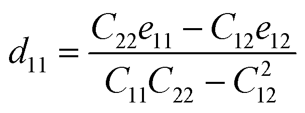 and
and  . The nonzero and independent Cij in the Voigt notation of FE MOX2 monolayers are given in Table 4, and they also are positive (i.e., C11, C22, C12, and C66 > 0), indicating their mechanical stability; our orthorhombic monolayers clearly satisfy the Born elastic stability criterion:51C11C22 − C122 > 0. Unlike 1H-type monolayers, MOX2 are anisotropic elastically (i.e., C11 ≠ C22 – Young's modulus (Y) and Poisson's ratio (ν) along the a-direction are also different from those along the b-direction; these are presented in the ESI.† Note that Y quantifies how easily a material can be stretched and deformed, whereas ν quantifies the deformation in the material in a direction perpendicular to the applied force's direction). We find large d11 for MOX2 monolayers – and small d12. However, the d12 of TiOCl2 or TiOBr2 is quite comparable with that of 1H-MoS2 (3.73 pm V−1)4 or 1H-VS2 (4.104 pm V−1).24 TiOBr2 has the largest d11 (37.758 pm V−1), which is 2–10 times larger than those of 1H-type monolayers4,6,8 (e.g., d11 of 1H-MoS2 and 1H-CrTe2 is 3.65 pm V−1 and 13.45 pm V−1, respectively6). This is because compared to 1H-type piezoelectrics, MOX2 have significantly larger e11 and relatively smaller elastic constants (e.g., the C11 of 1H-MoS2 is 130 N m−14). Note that the d11 of MOX2 is very similar to that of niobium oxyhalide monolayers (27.4 pm V−1 to 42.20 pm V−1).49 Interestingly, in comparison to bulk piezoelectric materials, we find that the piezo-response of MOX2 monolayers is remarkably strong. For example, the d11 (37.758 pm V−1) of TiOBr2 is an order of magnitude larger than that of α-quartz (d11 = 2.3 pmV−1)52 or the d33 of w-GaN (3.1 pm V−1);53 and also about 7 times higher than the d33 of w-AlN (5.1 pm V−1).53 Note that group-IV monochalcogenide monolayers19 have relatively smaller – indicating their softness – C11 and C22 (e.g., C11 = 20.87 N m−1 and C22 = 53.40 N m−1 for GeS monolayer19) than MOX2 monolayers. That is why group-IV monochalcogenide monolayers have larger d11 (e.g., d11 = 75.43 pm V−1 of the GeS monolayer)19 than that of MOX2.
| C 11 | C 22 | C 12 | C 66 | d 11 | d 12 | |
|---|---|---|---|---|---|---|
| VOF2(FM) | 67.999 | 96.795 | 15.073 | 22.404 | 29.028 | −0.753 |
| VOCl2(FM) | 53.761 | 58.255 | 8.711 | 18.808 | 29.575 | 0.239 |
| VOCl2(AFM1) | 50.810 | 42.460 | 6.887 | 18.640 | 31.545 | 1.045 |
| *VOCl2(FM) | 49.929 | 58.242 | 6.381 | 18.557 | 31.288 | 0.874 |
| VOBr2(FM) | 54.694 | 50.240 | 7.528 | 17.176 | 29.555 | −0.149 |
| VOBr2(AFM1) | 52.998 | 40.485 | 6.196 | 17.132 | 31.372 | 1.437 |
| *VOBr2(FM) | 53.134 | 51.124 | 5.935 | 17.021 | 30.779 | 2.054 |
| TiOCl2 | 78.264 | 56.536 | 8.318 | 16.971 | 33.753 | −3.700 |
| TiOBr2 | 76.942 | 47.862 | 6.879 | 15.029 | 37.758 | −3.768 |
As VOCl2 and VOBr2 monolayers have an AFM ground state, we also study how their piezo-response will change in response to the AFM-to-FM phase transition, which can be experimentally possible under an external magnetic field.54 Note that the FM-to-AFM transition can be a challenge in experiments. We find that the AFM1-to-FM transition somewhat increases the elastic constants – especially C22 – thus slightly decreases d11. Interestingly, such hardening of C22 is intrinsic to the AFM1-to-FM transition as we see that it comes from the mere magnetic order change even if the lattice parameters and atomic positions are fixed at AFM1 (see Table 4). There is a significant decrease in d12 (see Table 4). Interestingly, d12 changes its sign during the AFM1-to-FM transition for the VOBr2 monolayer, indicating that subject to an external electric field the monolayer can shrink or expand depending on the presence of a magnetic field. This can allow us to control piezoelectricity by magnetism, which may find applications in realizing multifunctional nano-devices. We believe that other magnetic piezoelectrics, especially 2D multiferroelectric, can also exhibit such coupling between piezo-response and magnetic order.
4 Conclusion
Our first principles calculations demonstrate that FE MOX2 monolayers have a strong in-plane piezoelectric response, which is not only significantly larger than that of the well-known 1H-type 2D piezoelectrics – e.g., both the e11 and d11 of MOX2 are about an order of magnitude larger than those of 1H-MoS2 – but also remarkably stronger than some of bulk piezoelectrics such as w-AlN or w-GaN. These monolayers also exhibit a remarkably large anisotropy in their piezo-response – i.e., piezo-response due to strain along the a-direction is about an order of magnitude larger than that of along the b-direction. We also show that a change in the magnetic order can change the piezo-response in multiferroelectric VOX2 monolayers, which can potentially couple piezoelectricity and magnetism. We believe that this work will inspire more research in searching for new piezoelectric materials that can couple strongly with magnetism. Also, such a large in-plane piezo-response can particularly be beneficial for 2D nanoscale flexible piezo-devices – e.g., actuators purely based on in-plane displacement.Conflicts of interest
There are no conflicts to declare.Acknowledgements
This publication has emanated from research conducted with the financial support of Science Foundation Ireland (SFI) under Grant Number 20/EPSRC/3710. The calculations were performed using the high-performance computing facilities of the Tyndall National Institute. The authors also acknowledge access to computing resources at the Irish Centre for High-End Computing (ICHEC).References
- Q. Zhang, S. Zuo, P. Chen and C. Pan, InfoMat, 2021, 3, 987–1007 CrossRef CAS.
- Y. Liu, E. T. N. Wahyudin, J.-H. He and J. Zhai, MRS Bull., 2018, 43, 959–964 CrossRef.
- G. Michael, Y. Zhang, J. Nie, D. Zheng, G. Hu, R. Liu, M. Dan, L. Li and Y. Zhang, Nano Energy, 2020, 76, 105091 CrossRef CAS.
- K.-A. N. Duerloo, M. T. Ong and E. J. Reed, J. Phys. Chem. Lett., 2012, 3, 2871–2876 CrossRef CAS.
- H. Zhu, Y. Wang, J. Xiao, M. Liu, S. Xiong, Z. J. Wong, Z. Ye, Y. Ye, X. Yin and X. Zhang, Nat. Nanotechnol., 2015, 10, 151–155 CrossRef CAS PubMed.
- M. N. Blonsky, H. L. Zhuang, A. K. Singh and R. G. Hennig, ACS Nano, 2015, 9, 9885–9891 CrossRef CAS PubMed.
- K. H. Michel, D. Çakir, C. Sevik and F. M. Peeters, Phys. Rev. B, 2017, 95, 125415 CrossRef.
- M. M. Alyoruk, Y. Aierken, D. Çakır, F. M. Peeters and C. Sevik, J. Phys. Chem. C, 2015, 119, 23231–23237 CrossRef CAS.
- Y. Lu and S. B. Sinnott, ACS Appl. Nano Mater., 2020, 3, 384–390 CrossRef CAS.
- P. Nandi, A. Rawat, R. Ahammed, N. Jena and A. De Sarkar, Nanoscale, 2021, 13, 5460–5478 RSC.
- S.-D. Guo, Y.-T. Zhu, K. Qin and Y.-S. Ang, Appl. Phys. Lett., 2022, 120, 232403 CrossRef CAS.
- Z. Kahraman, A. Kandemir, M. Yagmurcukardes and H. Sahin, J. Phys. Chem. C, 2019, 123, 4549–4557 CrossRef CAS.
- M. T. Ong and E. J. Reed, ACS Nano, 2012, 6, 1387–1394 CrossRef CAS PubMed.
- M. T. Ong, K.-A. N. Duerloo and E. J. Reed, J. Phys. Chem. C, 2013, 117, 3615–3620 CrossRef CAS.
- H. J. Kim, M. Noor-A-Alam and Y.-H. Shin, J. Appl. Phys., 2015, 117, 145304 CrossRef.
- M. Noor-A-Alam, H. J. Kim and Y.-H. Shin, J. Appl. Phys., 2015, 117, 224304 CrossRef.
- M. Noor-A-Alam, H. J. Kim and Y.-H. Shin, Phys. Chem. Chem. Phys., 2014, 16, 6575–6582 RSC.
- R. Ahammed, N. Jena, A. Rawat, M. K. Mohanta, Dimple and A. De Sarkar, J. Phys. Chem. C, 2020, 124, 21250–21260 CrossRef CAS.
- R. Fei, W. Li, J. Li and L. Yang, Appl. Phys. Lett., 2015, 107, 173104 CrossRef.
- L. Zhang, C. Tang, C. Zhang and A. Du, Nanoscale, 2020, 12, 21291–21298 RSC.
- M. K. Mohanta, F. IS, A. Kishore and A. De Sarkar, ACS Appl. Mater. Interfaces, 2021, 13, 40872–40879 CrossRef PubMed.
- Y. Zhou, D. Wu, Y. Zhu, Y. Cho, Q. He, X. Yang, K. Herrera, Z. Chu, Y. Han, M. C. Downer, H. Peng and K. Lai, Nano Lett., 2017, 17, 5508–5513 CrossRef CAS PubMed.
- J. Yang, A. Wang, S. Zhang, J. Liu, Z. Zhong and L. Chen, Phys. Chem. Chem. Phys., 2019, 21, 132–136 RSC.
- M. Noor-A-Alam and M. Nolan, ACS Appl. Electron. Mater., 2022, 4, 850–855 CrossRef CAS PubMed.
- Y. Zhao, L. Lin, Q. Zhou, Y. Li, S. Yuan, Q. Chen, S. Dong and J. Wang, Nano Lett., 2018, 18, 2943–2949 CrossRef CAS PubMed.
- C. Huang, Y. Du, H. Wu, H. Xiang, K. Deng and E. Kan, Phys. Rev. Lett., 2018, 120, 147601 CrossRef PubMed.
- Q. Yang, W. Xiong, L. Zhu, G. Gao and M. Wu, J. Am. Chem. Soc., 2017, 139, 11506–11512 CrossRef CAS PubMed.
- Z. Tu, M. Wu and X. C. Zeng, J. Phys. Chem. Lett., 2017, 8, 1973–1978 CrossRef CAS PubMed.
- J. Qi, H. Wang, X. Chen and X. Qian, Appl. Phys. Lett., 2018, 113, 043102 CrossRef.
- X. Feng, J. Liu, X. Ma and M. Zhao, Phys. Chem. Chem. Phys., 2020, 22, 7489–7496 RSC.
- W. Luo, K. Xu and H. Xiang, Phys. Rev. B, 2017, 96, 235415 CrossRef.
- J.-J. Zhang, L. Lin, Y. Zhang, M. Wu, B. I. Yakobson and S. Dong, J. Am. Chem. Soc., 2018, 140, 9768–9773 CrossRef CAS PubMed.
- H. Ai, X. Song, S. Qi, W. Li and M. Zhao, Nanoscale, 2019, 11, 1103–1110 RSC.
- H. Tan, M. Li, H. Liu, Z. Liu, Y. Li and W. Duan, Phys. Rev. B, 2019, 99, 195434 CrossRef CAS.
- H.-P. You, N. Ding, J. Chen and S. Dong, Phys. Chem. Chem. Phys., 2020, 22, 24109–24115 RSC.
- C. Xu, P. Chen, H. Tan, Y. Yang, H. Xiang and L. Bellaiche, Phys. Rev. Lett., 2020, 125, 037203 CrossRef CAS PubMed.
- N. Ding, J. Chen, S. Dong and A. Stroppa, Phys. Rev. B, 2020, 102, 165129 CrossRef CAS.
- N. A. Hill, J. Phys. Chem. B, 2000, 104, 6694–6709 CrossRef CAS.
- G. Kresse and J. Furthmüller, Phys. Rev. B: Condens. Matter Mater. Phys., 1996, 54, 11169 CrossRef CAS PubMed.
- G. Kresse and D. Joubert, Phys. Rev. B: Condens. Matter Mater. Phys., 1999, 59, 1758 CrossRef CAS.
- J. P. Perdew, K. Burke and M. Ernzerhof, Phys. Rev. Lett., 1996, 77, 3865 CrossRef CAS PubMed.
- A. Togo and I. Tanaka, Scr. Mater., 2015, 108, 1–5 CrossRef CAS.
- S. L. Dudarev, G. A. Botton, S. Y. Savrasov, C. J. Humphreys and A. P. Sutton, Phys. Rev. B: Condens. Matter Mater. Phys., 1998, 57, 1505–1509 CrossRef CAS.
- P. Ghosez, J.-P. Michenaud and X. Gonze, Phys. Rev. B: Condens. Matter Mater. Phys., 1998, 58, 6224–6240 CrossRef CAS.
- M. Wu and X. C. Zeng, Nano Lett., 2016, 16, 3236–3241 CrossRef CAS PubMed.
- H. Wang and X. Qian, 2D Mater., 2017, 4, 015042 CrossRef.
- M. Noor-A-Alam, O. Z. Olszewski and M. Nolan, ACS Appl. Mater. Interfaces, 2019, 11, 20482–20490 CrossRef CAS PubMed.
- F. Bernardini, V. Fiorentini and D. Vanderbilt, Phys. Rev. B: Condens. Matter Mater. Phys., 1997, 56, R10024–R10027 CrossRef CAS.
- Y. Wu, I. Abdelwahab, K. C. Kwon, I. Verzhbitskiy, L. Wang, W. H. Liew, K. Yao, G. Eda, K. P. Loh, L. Shen and S. Y. Quek, Nat. Commun., 2022, 13, 1884 CrossRef CAS PubMed.
- T. Cheiwchanchamnangij and W. R. L. Lambrecht, Phys. Rev. B: Condens. Matter Mater. Phys., 2012, 85, 205302 CrossRef.
- F. Mouhat and F.-X. Coudert, Phys. Rev. B: Condens. Matter Mater. Phys., 2014, 90, 224104 CrossRef.
- R. Bechmann, Phys. Rev., 1958, 110, 1060–1061 CrossRef.
- C. M. Lueng, H. L. W. Chan, C. Surya and C. L. Choy, J. Appl. Phys., 2000, 88, 5360–5363 CrossRef CAS.
- L. V. B. Diop, T. Faske, O. Isnard and W. Donner, Phys. Rev. Mater., 2021, 5, 104401 CrossRef CAS.
Footnote |
| † Electronic supplementary information (ESI) available: Phonon band structures of MOX2 monolayers in paraelectric and ferroelectric phases, phonon band structures of the TiOF2 monolayer, Young's modulus and Poisson's ratio, GGA+Ueff calculations for eij, Cij, and dij, structural and piezoelectric properties of VOCl2(AFM3) and VOBr2(AFM3). See DOI: https://doi.org/10.1039/d2nr02761e |
| This journal is © The Royal Society of Chemistry 2022 |