
 Open Access Article
 This Open Access Article is licensed under a
 Creative Commons Attribution 3.0 Unported Licence
Transparent electronic and photoelectric synaptic transistors based on the combination of an InGaZnO channel and a TaOx gate dielectric†
Yuanbo
Li
 *a,
Tupei
Chen
a,
Xin
Ju
*a and
Teddy
Salim
b
*a,
Tupei
Chen
a,
Xin
Ju
*a and
Teddy
Salim
b
aSchool of Electrical and Electronic Engineering, Nanyang Technological University, 639798, Singapore. E-mail: YUANBO001@e.ntu.edu.sg; ju0002in@e.ntu.edu.sg
bSchool of Materials Science and Engineering, Nanyang Technological University, 639798, Singapore
First published on 1st July 2022
Abstract
A transparent thin film transistor (TFT) based on the combination of an InGaZnO channel and a high-κ (the dielectric constant is about 42.6) TaOx gate dielectric layer is fabricated. The TFT shows robust anticlockwise hysteresis under DC voltage sweep and synaptic behaviors (i.e., excitatory postsynaptic current, short-term memory plasticity, short-term memory to long-term memory transition, and potentiation and depression) under voltage pulse stimulus. In addition, the TFT shows high responsivity to illumination of light with various wavelengths (ultraviolet and visible light). Synaptic behaviors in response to light pulse stimuli, which could be employed in vision-based neuromorphic applications, are demonstrated. Large conductance change (Gmax/Gmin > 10) and ultra-low non-linearity (α < 0.5) of the potentiation and depression can be inspired by either gate bias pulses or photoelectric pulses with short pulse widths and small amplitudes.
1. Introduction
Artificial synaptic devices have been attracting growing attention since the conventional von Neumann architecture was confronted with a bottleneck, especially in the emerging neuromorphic computing area.1–3 To characterize a synapse, there are several fundamental indices: excitatory postsynaptic current (EPSC), short-term memory (STM) plasticity, STM transition to long-term memory (LTM), and potentiation and depression (P/D).4–6 The EPSC refers to the opening of ion gates in the channel of a postsynaptic cell and the strengthening of synaptic transmission in response to an external stimulus applied to the presynaptic cell. STM plasticity reflects the tunability of the synaptic weight in response to different presynaptic activities. For instance, paired-pulse facilitation (PPF) is a typical form of STM plasticity, which shows the impact of the time interval between two successive pulse stimuli on the amplification of the EPSC. To extend the decay of the EPSC in STM and achieve the transition from STM to LTM, multiple repeated stimulus pulses can be applied, which evolves the synapse function from simple learning to the concurrence of learning and memory. With further increase of the stimuli pulse number, P/D of the synaptic strength could happen.7An indium gallium zinc oxide (IGZO)-based thin-film transistor (TFT) is a promising candidate for an artificial synapse, which could be attributed to the following superiorities. (1) As a three-terminal synapse, conductance change controlled by the gate terminal and signal transmission through the semiconductor channel layer can be achieved concurrently in an IGZO TFT, which improves the efficiency of the learning process compared with two-terminal synapses.6 (2) The conductance of the IGZO channel can be modulated by the carrier concentration effectively thanks to the potential-model based carrier transport mechanism in IGZO.8 Meanwhile, the incorporation of stabilizer Ga balances the excess carrier concentration in In- and Zn-based oxides, which enhances the gate controllability over the channel conductance.9 (3) IGZO has a large bandgap at around 3.2 eV, facilitating an IGZO TFT to be applied as a highly transparent artificial synapse. (4) IGZO is compatible with a large variety of dielectrics regardless of the valence band offset between each other, which benefits from the inhibited transport of holes in IGZO.10 (5) Amorphous IGZO can be deposited by RF magnetron sputtering at room temperature with good uniformity, which makes an IGZO TFT very suitable for use in large-area arrays fabricated on flexible substrates. (6) In contrast to some metal–oxide based two-terminal synaptic devices (e.g., memristors or resistive random-access memory (ReRAM)) which show large device-to-device variations,11 an IGZO TFT has a small device-to-device variation. (7) IGZO is sensitive to light in a specific wavelength range, which makes the output current of IGZO TFTs tunable by external light illumination.12–14
Either electronic or photoelectric IGZO synaptic TFTs have been reported based on different working principles. Ferroelectric IGZO TFTs are used to emulate the electronic synapses by gradually modulating the direction of polarization in the ferroelectric layer under the stimulation of electric pulses.15,16 The main limitations for ferroelectric IGZO synaptic TFTs are: (1) a large amplitude of the electric pulse is required to inspire the reverse of polarization and (2) the deposition of a ferroelectric layer needs precise thickness control and high temperature annealing. Charge-trapping based IGZO synaptic TFTs are also demonstrated with a variety of defect-rich dielectrics. A SiOx-based double-gate IGZO synaptic TFT was presented in ref. 17, which showed electro-sensitivity based on charge trapping/release and photo-sensitivity under UV stimulation. The charge-trapping effect inspired the inhibited postsynaptic current (IPSC), while UV illumination stimulated the EPSC. The IPSC and EPSC could be transformed mutually by changing the predominance between electric pulses and UV pulses. An optoelectronic synaptic TFT based on the combination of an IGZO channel and an alkylated graphene oxide (GO) charge-trapping layer has been developed in ref. 18. The mixture of UV light pulses and electric pulses accelerated the release of trapped carriers in alkylated GO, which enlarges the ratio of maximum conductance (Gmax)/minimum conductance (Gmin) with retained small non-linearity in P/D of the synapse. Oxygen-deficient HfOx is a special material which exhibits charge-trapping effect and ferroelectricity at the same time. In ref. 19, W. Yang et al. investigated an IGZO synaptic transistor with bipolar plasticity based on an HfOxNy/HfOx/HfOxNy sandwich-stack dielectric structure. Positive electric pulses stimulated the IPSC by the charge trapping/release effect, while negative electric pulses stimulated the EPSC by the ferroelectric effect. This bipolar plasticity could emulate the distinct response of neurons to the stimuli (i.e., favorite or unwanted). Some drawbacks of charge-trapping synaptic TFTs include the following: (1) the EPSC could hardly be excited by electric pulses directly since the carrier concentration in IGZO is reduced with the charge trapping effect which leads to the positive shift of the threshold voltage (Vth) of the IGZO TFT; (2) the memory window induced by charge trapping is small, resulting in the small Gmax/Gmin ratio in P/D of the synapse; and (3) charge-trapping effects are not enduring and stable without special structure engineering.
An ion-conductive dielectric is also an emerging candidate to be applied in IGZO synaptic TFTs, which contains movable ions to emulate the neurotransmitters in the synaptic cleft. The proton-rich chitosan electrolyte deposited by spin-coating is widely employed as the gate insulator in photoelectric synaptic IGZO TFTs.20,21 Protons inside chitosan will migrate to the IGZO/chitosan interface driven by positive electric pulses, which excites the EPSC flowing through the IGZO accumulation layer. STM plasticity, STM transition to LTM, and P/D are all successfully mimicked under the synergistic modulation of electric and light pulses. However, organic chitosan could induce serious instability and poor endurance of the device. In addition, an organic material is not compatible with the complementary-metal–oxide–semiconductor (CMOS) process. TaOx is a high-κ ion-conductive dielectric which has been extensively used in ReRAM as a resistance switching layer.22–24 Pure electronic metal–oxide synaptic TFTs have been reported by utilizing TaOx as a gate insulator.25,26 In this work, a staggered bottom-gate IGZO synaptic TFT with the TaOx dielectric was demonstrated with high stability and endurance. A large Gmax/Gmin ratio and small non-linearity were achieved in P/D of the synaptic strength under the stimulation of pure electric pulses with small voltage amplitudes and short pulse widths thanks to the abundant free ions and high dielectric constant of the sputtering-deposited TaOx layer. By applying negative pulses with step-increasing amplitudes for the depression, the non-linearity of depression and the endurance of the Gmax/Gmin ratio under repeated P/D cycles were improved significantly. On the other hand, the synaptic behaviors including the EPSC, STM plasticity, STM transition to LTM, P/D with a large Gmax/Gmin ratio and small non-linearity were successfully mimicked under the stimulation of either UV or visible light pulses (here, for the visible light experiment, blue, green, and red light with wavelengths of 470 nm, 525 nm, and 633 nm, respectively, were used). The transparent IGZO TFT of this work is promising in vision-based neuromorphic applications with high learning accuracy.27,28
2. Experimental methods
2.1. Device fabrication
The bottom-gate-top-contact (BGTC) structure was chosen for TFT fabrication. In this structure, the dielectric layer (160 nm TaOx), channel layer (45 nm IGZO), source/drain (S/D) electrodes (200 nm ITO) and passivation layer (100 nm SiO2) were deposited on the ITO-coated (bottom-gate) glass layer by layer. Deposition of the TaOx, IGZO and ITO (S/D electrodes) layers were all carried out by RF magnetron sputtering with 100 W RF power at room temperature under a pure Ar atmosphere. The Ar flow rates for the sputtering deposition of TaOx, IGZO and ITO were set to 100, 50 and 20 sccm, respectively. Plasma-enhanced chemical vapor deposition (PECVD) was utilized for the deposition of the SiO2 passivation layer. To define the patterns of the channel layer and S/D contacts, photolithography and a lift-off process were applied. Finally, to stabilize the carrier concentration in the channel layer, the as-fabricated device was annealed at 300 °C under a N2 atmosphere for 1 hour. It is worth mentioning that the thermal budgets of all processes were controlled at or below 300 °C. The process flow is shown in Fig. S1 (ESI†). To measure the dielectric constant of the TaOx layer, a capacitor with an ITO–TaOx–ITO sandwich structure was fabricated with a dielectric thickness of 160 nm and an overlap area between the top electrode and bottom electrode of 100 × 100 μm2, as shown in Fig. S2 (ESI†).2.2. Device and materials characterization
The surface roughness of the TaOx layer was measured using an atomic force microscope (AFM) from Bruker. The 2D morphology of the TaOx layer is shown in Fig. S3 (ESI†). Electrical characteristics (including current–voltage transfer characteristics, and capacitance–voltage relationships) of the device and their response to the stimulation of voltage or light pulses were measured with a Keithley 4200 semiconductor characterization system (SCS). A LIGHTNINGCURE Spotlight source LC8 was used to deliver UV light in the wavelength range of 300–400 nm. A SugarCUBE ULTRA LED light source was used to provide visible light at different wavelengths (here, blue, green, and red light with wavelengths of 470 nm, 525 nm, and 633 nm, respectively, were used) for the experiment of examining the wavelength selectivity of the synaptic behaviors in the as-fabricated TFT. In addition, X-ray photoelectron spectroscopy (XPS) analysis of the as-deposited TaOx layer was performed using an AXIS Supra spectrometer (Kratos Analytical Inc., UK) equipped with a hemispherical analyser and a monochromatic Al K-alpha source (1487 eV) operated at 15 mA and 15 kV. XPS depth profiling experiments were carried out using an argon Gas Cluster Ion Source (GCIS, Kratos Analytical Inc. Minibeam 6). The ion beam was rastered over an area of 1 × 1 mm2. To minimize the preferential sputtering of oxygen from TaOx, Arn+ with a cluster size (n) of 1000 and an incident energy of 10 keV was employed. The XPS spectra were acquired at a pass energy of 20 eV after each etching cycle (30 min). A 3.1-volt bias was applied to the sample to neutralise the charge build-up on the sample surface. The binding energies (BEs) were charge-corrected based on the C 1s peak of adventitious carbon at 284.8 eV.3. Results and analysis
Fig. 1(b) shows the schematic diagram of the IGZO TFT device, which can be used to mimic the human brain synapse shown in Fig. 1(a). The bottom-gate (ITO) applied with positive electric pulses (A) or the light pulses shining on the whole device (B) played a role as the presynaptic cell. Then, the ITO (D)–IGZO–ITO (S) structure of the TFT could be regarded as the postsynaptic cell where the drain current (IDS) would flow through. IDS represented the EPSC. The region between the presynaptic and postsynaptic cells is called the synaptic cleft where neurotransmitters are released and stimulate the EPSC change in the postsynaptic cell. In this device, the dielectric layer TaOx was expected to be the ‘cleft’, where neurotransmitter-like species would be created under external stimuli. Electrical and illumination pulses were applied respectively to evaluate the device synaptic behavior.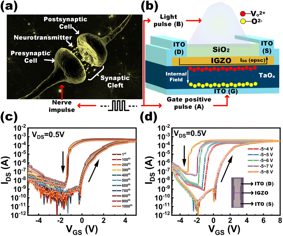 | ||
| Fig. 1 (a) Schematic illumination of the human brain synapse (modified based on ref. 29). (b) 3D schematic diagram of the IGZO TFT device of this work. (c) Transfer curves of the TFT under −5–5 V DC dual sweep with 1000 cycles. (d) Transfer curves of the TFT (the same device as in (c)) under DC sweep with different positive stop voltages. The channel width (W) and length (L) of the TFT are 80 and 5 μm, respectively. The inset in (d) is an optical image of the practical device. | ||
3.1. Electronic synapse
The following electrical characterization was conducted for the TFT device. Firstly, DC dual sweep was applied to the TFT. Fig. 1(c) shows the transfer curves of the TFT under 103 cycles of bottom-gate voltage (VGS) dual sweep from −5 V to 5 V. The drain voltage (VDS) was fixed at 0.5 V. A robust hysteresis between the forward sweep and backward sweep can be observed in Fig. 1(c). The memory window (i.e., the difference in the threshold voltage Vth of the TFT between the forward sweep and backward sweep) was maintained at around 3.2 V. Furthermore, as the positive stop voltage of the DC sweep increased, the memory window tended to enlarge, as shown in Fig. 1(d). The capacitance–voltage (C–V) measurement was also carried out with the ITO–TaOx–ITO capacitor structure. The measured capacitance was 23.58 pF at a frequency of 100 kHz. Thus, the dielectric constant at 100 kHz of the TaOx layer was 42.6. A schematic diagram of the capacitor structure and the result of the C–V measurement are shown in Fig. S2 (ESI†). The gate leakage current IG under the DC sweep is shown in Fig. S4.† It varied between tens of pA and hundreds of nA at a gate voltage of −5 V to +5 V, and it reached a maximum of close to 1 μA at VGS = 5 V. The subthreshold swing (S.S.) of the TFT at a drain current IDS = 1 nA was 50 and 150 mV dec−1 for the forward sweep and backward sweep, respectively. S.S. was determined by the oxide capacitance, interface trap density and semiconductor depletion capacitance as shown in eqn (1):30S.S. = (ln![[thin space (1/6-em)]](https://www.rsc.org/images/entities/char_2009.gif) 10)(kT/q)[(Cox + CD + Cit)/Cox] 10)(kT/q)[(Cox + CD + Cit)/Cox] | (1) |
The stable anticlockwise hysteresis under the DC sweep of the TFT indicated that there existed active ion movement in the dielectric layer driven by the applied electric field.33,34 Another evidence of the ion movement in the dielectric layer was the flat band voltage (VFB) shift and slope change in the gate–source capacitance (CGS) measurements in the VGS sweep in the range of −5–5 V.35,36 The schematic of the configuration and results of the CGS measurement are shown in Fig. S5 (ESI†).
The XPS results of the as-deposited TaOx layer are shown in Fig. 2(a)–(d). From Fig. 2(a), it can be seen that the O/Ta ratio in TaOx was around 2.15, which means that TaOx is oxygen-deficient. The atomic concentration of each species in the TaOx layer in each etching cycle is given in Table S2 (ESI†). Fig. 2(b) depicts the wide scan of the bulk of TaOx from 0 to 1200 eV in the 7th etching cycle. The Ta 4f spectra in Fig. 2(c) shows that there existed dominant Ta4+ species in combination with a small amount of Ta3+ species, which matched well with the O/Ta ratio. Furthermore, Fig. 2(d) shows the O 1s spectra in the bulk of TaOx, which was deconvoluted into two peaks, i.e., the dominant Ta–O peak (OL) with a binding energy of 530.1 eV and the oxygen vacancy (VO) peak with a binding energy of 531.6 eV. From the above four figures, we could confirm that the as-deposited TaOx contained oxygen ions. The profiles of Ta 4f spectra and O 1s spectra with the etching cycle are shown in Fig. S6 (ESI†).
 | ||
| Fig. 2 (a) Atomic concentration (left y-axis) and O/Ta ratio (right y-axis) in the as-deposited TaOx layer. (b) Wide scan of the bulk TaOx in the 7th etching cycle. (c) Ta 4f spectra in the bulk of TaOx, deconvoluted into two Ta4+ and Ta3+ peaks. (d) O 1s spectra in the bulk of TaOx, deconvoluted into lattice oxygen (OL) and oxygen vacancy (OV). (e) EPSC of the TFT under the stimulation of a positive gate pulse with an amplitude of 5 V, pulse width of 30 ms, and base level of 0.1 V, followed by a negative gate pulse with an amplitude of 3 V, pulse width of 30 ms, and base level of 0.1 V. (f) Band diagrams of the TFT showing the ion movements in TaOx layer under different stages. | ||
To explore the detailed ion movements in the TaOx layer under electric signals, a positive electric pulse with an amplitude of 5 V, pulse width of 30 ms, and base level of 0.1 V, followed by a negative pulse with an amplitude of 3 V, pulse width of 30 ms, and base level of 0.1 V was applied to the bottom-gate. According to the polarity of the applied voltage and different responses of IDS (Fig. 2(e)), the status of the device could be categorized into three stages. The band diagrams in the three stages (positive bias, base level, and negative bias) are shown in Fig. 2(f). The bandgap of IGZO is around 3.2 eV and the bandgap of TaOx is around 3.7 eV.37 At stage 1, the positive bias 5 V provided an external field, attracting negatively charged oxygen ions O2− which existed in the as-deposited oxygen-deficient TaOx layer to the TaOx/bottom-gate interface, and driving the oxygen vacancy ions Vo2+ in the TaOx layer to the TaOx/IGZO interface.25,38 These accumulated Vo2+ together with the large positive bias attracted a large amount of electrons in the IGZO layer to the interface, contributing to the large EPSC spike. At stage 2, under a base level of 0.1 V, the segregated Vo2+ and oxygen ions (O2−) started to recombine slowly with the nearly-zero external field. Still, there remained some Vo2+ near the interface, forming an internal field inside the TaOx layer. The remaining Vo2+ kept attracting electrons in the IGZO layer to the interface, which slowed down the EPSC decay. At stage 3, the negative bias −3 V accelerated the recombination of Vo2+ and O2−, pulling the EPSC to an extremely low level.
To further evaluate the synaptic behaviours of the TFT, voltage pulses with different pulse widths, periods, and amplitudes were applied to the bottom-gate. Firstly, to investigate the short-term memory (STM) and the plasticity of the TFT, three experiments were conducted accordingly as described below, and all the results are summarized in Fig. 3.
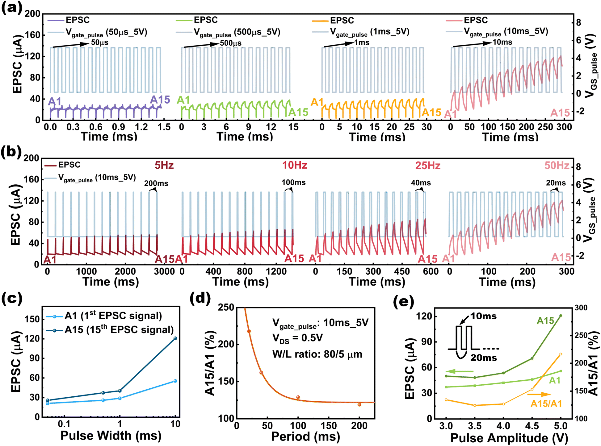 | ||
| Fig. 3 (a) EPSC under stimulation of 15 consecutive voltage pulses for different pulse widths. A1 and A15 denote the current spike in response to the 1st and 15th VGS pulse, respectively. (b) EPSC under the stimulation of 15 consecutive pulses with the pulse width of 10 ms for different pulse periods (pulse frequencies). (c) The 1st and 15th EPSC signals as a function of the pulse width. (d) A15/A1 EPSC ratio vs. pulse period. (e) The 1st and 15th EPSC signals and A15/A1 EPSC ratio vs. pulse amplitude. Note: Pulse amplitude in (a)–(d) is 5 V; base level of pulses in (a)–(e) is 0.1 V. | ||
In the first experiment, four sets of 15 consecutive pulses with the same amplitude (5 V) and base level (0.1 V) were applied to the gate terminal. Each set of pulses had a different pulse width (50 μs, 500 μs, 1 ms and 10 ms), but the same duty ratio (50%). The first EPSC signal and fifteenth EPSC signal were denoted as A1 and A15, respectively. As shown in Fig. 3(a), with the increase of the pulse width, the EPSC signal became stronger. The trend of A1 and A15 with the pulse width is depicted in Fig. 3(c). When the pulse width increased from 50 μs to 1 ms, the EPSC signals of both A1 and A15 and the EPSC ratio of A15/A1 all increased gradually. There was a large increase in the EPSC signals of both A1 and A15 and the EPSC ratio for the pulse width of 10 ms.
In the second experiment, four sets of 15 consecutive pulses with the same amplitude (5 V), base level (0.1 V), and pulse width (10 ms) were applied to the gate terminal, but the pulse frequency fp was different for a different set of pulses (i.e., fp was 5, 10, 25, and 50 Hz for the four sets of pulses, respectively). The A1–A15 EPSC for different fp is shown in Fig. 3(b), and the relationship between the A15/A1 EPSC ratio and pulse period fp−1 (= 20, 40, 100, and 200 ms) is shown in Fig. 3(d). As the period of the pulse increased, the A15/A1 EPSC ratio decreased and remained almost unchanged for a period longer than 100 ms.
In the third experiment, five sets of 15 consecutive pulses with the same base level (0.1 V), pulse width (10 ms), and pulse period (20 ms) were applied to the gate terminal, but the amplitude of the pulses was increased from 3 V to 5 V with a step of 0.5 V. The result is shown in Fig. 3(e). It can be observed from the figure that the A1 EPSC increased with the pulse amplitude gently, but both the A15 EPSC and A15/A1 EPSC ratio showed a trend of large increase starting at 4 V. From the above three test schemes, the electrical pulse widths, periods, and amplitudes all showed the capability to modulate the EPSC signal strength and STM retention time. The transition from STM to long-term memory (LTM) of the device was achieved with 5 consecutive pulses with an amplitude of 5 V, pulse width of 30 ms, and base level of 0.5 V. Under the stimulation of the positive voltage pulses, the EPSC of the device lasts in the high level for more than one minute as shown in Fig. S7 (ESI†).
Besides STM plasticity, the capability to strengthen or weaken the EPSC signal in response to different activities was another important property of the synapse, i.e., the synaptic potentiation and depression (P/D). The most significant parameters to evaluate the P/D performance of the synapse were the Gmax/Gmin ratio, non-linearity, and asymmetry of non-linearity between potentiation and depression. (1) The Gmax/Gmin ratio is the ratio of the maximum of the EPSC and minimum of the EPSC in P/D in essence. A large Gmax/Gmin ratio (>10) is favourable which is the basis of high accuracy (>80%) of the neural network.39 (2) Non-linearity α of P/D also determines the learning accuracy of the neural network. Usually, small α (<0.5–1) of P/D means the weight change of the synapse under P/D is nearly linear, and the learning accuracy could exceed 80%.40 (3) Asymmetry of α indicates the symmetric characteristics of P/D, which is equal to the absolute difference value of αP and αD. Zero value of the asymmetry implies the perfect symmetric characteristics of P/D.41 To verify whether the TFT could realize the synaptic P/D and evaluate the characteristics of P/D, 50 positive pulses with an amplitude of 1.8 V and pulse width of 30 ms, and negative pulses with an amplitude of 1 V and pulse width of 30 ms were applied to the gate terminal successively. The EPSC was read at the base level (0.1 V) of each pulse. As shown in Fig. 4(a), the EPSC of the TFT increased from 62.16 nA to 1.55 μA under the repeated positive pulses and reduced back to 63.52 nA under the repeated negative pulses. The calculation of the Gmax/Gmin ratio was straightforward, which was equal to 24.9. To derive the value of αP (for potentiation) and αD (for depression), the following exponential fitting model was adopted:42
| G = λexp(αx + β) + γ | (2) |
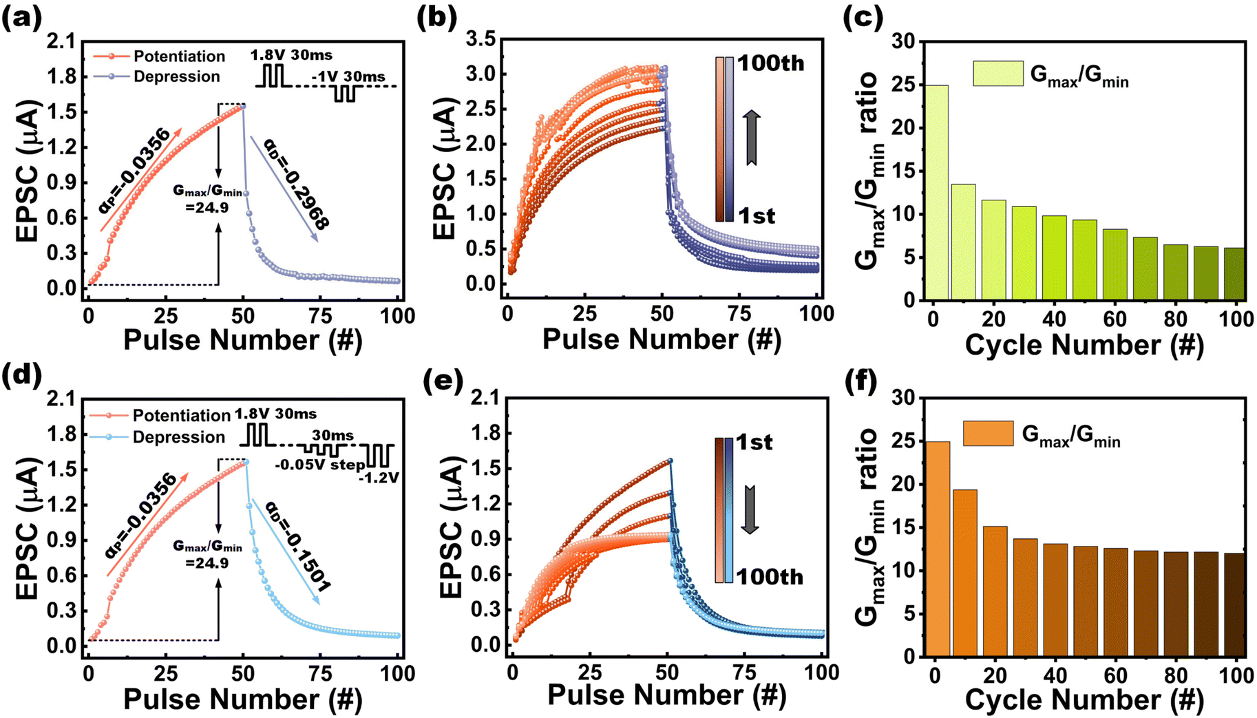 | ||
| Fig. 4 (a) The P/D of the synapse under stimulation of 50 consecutive positive voltage pulses with amplitude of 1.8 V and pulse width of 30 ms, followed by 50 consecutive negative voltage pulses with amplitude of 1 V and pulse width of 30 ms. The base level of all pulses was fixed at 0.1 V. (b) Endurance of P/D under 100 cycles with the pulse schemes used in (a). (c) Gmax/Gmin ratio as a function of P/D cycle with the pulse schemes used in (a). (d) P/D of the synapse under stimulation of 50 consecutive positive voltage pulses with amplitude of 1.8 V and pulse width of 30 ms, followed by 50 consecutive negative voltage pulses with step-increasing amplitudes from 0.05 V to 1.2 V and a pulse width of 30 ms. The base level of all pulses was fixed at 0.1 V. (e) Endurance of the P/D under 100 cycles with the pulse schemes used in (d). (f) Gmax/Gmin ratio versus the P/D cycle with the pulse schemes used in (d). | ||
In eqn (2), G is the conductance or the EPSC value of the synapse, x is the number of pulse, α is the non-linearity of potentiation or depression, and λ, β, and γ are the fitting coefficients. Fitting to the experimental data was conducted in MATLAB. The fitting showed that αP was −0.0356 and αD was −0.2968, as shown in Fig. S8(a) and (b) (ESI†). Correspondingly, the asymmetry |αp − αD| of the P/D under the proposed stimulation scheme was 0.2612. αD was about 10 times higher than αP, which resulted in a large asymmetry of the P/D. To evaluate the endurance of the synaptic behavior under the stimulation of pure electronic pulses, 100 repeated P/D cycles were applied to the TFT. Fig. 4(b) and (c) show the test results. Both Gmax and Gmin increased with the P/D cycle, but the Gmax/Gmin ratio decreased to lower than 10 after 50 cycles. This could be due to the inefficient depression by the negative pulses with a fixed amplitude. To alleviate the extremely deteriorated Gmax/Gmin ratio under repeated P/D cycles, reduce the absolute value of the depression non-linearity and shrink the asymmetry of the P/D, depression by 50 consecutive negative voltage pulses with step-increasing amplitudes was applied.41 The amplitude of the negative pulses was set to 0.05 V initially; then it increased with a fixed step of 0.05 V until 1.2 V. The amplitude of the rest 26 pulses was fixed at 1.2 V. As shown in Fig. 4(d), αD was improved from −0.2968 to −0.1501, and thus, the asymmetry of the P/D shrunk from 0.2612 to 0.1145. In Fig. 4(e), the Gmax of the P/D showed a downward shift with applied cycles, while the Gmin showed little change. As shown in Fig. 4(f), the Gmax/Gmin ratio was maintained at around 12 after 100 cycles. The gradual reduction of Gmax suggests that there still existed a slight charge-trapping effect due to the non-passivated defect states in the interface region.
3.2. Photoelectric synapse
Besides the pure electrical signal, light pulses with specific wavelengths could also inspire the synaptic behaviour of the TFT by changing carrier concentration in the IGZO layer. In this work, several illumination scenarios have been adopted to excite and modulate the EPSC in the TFT, i.e., UV light with the wavelength range of 300–400 nm, and visible light (i.e., blue, green, and red light with wavelengths of 470 nm, 525 nm, and 633 nm, respectively), were used.UV light is well known as a source to produce photon-generated electron–hole pairs in the IGZO TFT. The drain current IDS, namely the EPSC, could be modulated at a low and fixed gate bias under UV illumination. To evaluate the STM plasticity under photoelectric pulses, the UV light pulses with different irradiance and pulse widths were shone on the TFT. Fig. 5(a) and (b) show the modulation of the EPSC signals by UV irradiation with various intensities (i.e., 1350, 2250, 3150 and 4500 mW cm−2) and various UV pulse widths (i.e., 100, 200, 300, 400, 500 ms), respectively. As can be seen from the figures, a higher UV irradiance and larger pulse width could both enhance the STM of the TFT. To investigate the paired pulse facilitation (PPF) property of the TFT, the TFT was exposed to 2 consecutive UV pulses with the irradiance of 4500 mW cm−2, a pulse width of 100 ms and various time intervals (in terms of pulse period Δt = 200, 400, 500, 1000, 2000 and 5000 ms). A1 and A2 represented the first and second EPSC signals, respectively. The ratio of A2/A1 was defined as the PPF index, reflecting the STM plasticity of the synapse. Fig. 5(c) depicts the PPF index vs. the time interval of the two pulses. The highest value of the PPF index was 145% at the shortest time interval (i.e., Δt = 200 ms); and the PPF index decayed with the increase of the time interval. Finally, the P/D property of the TFT was tested with successive 25 pulses of the UV light followed by 25 pulses of the negative gate bias. For potentiation, the UV light pulses had irradiance of 4500 mW cm−2 and a pulse width of 100 ms, and the base level was 0.1 V. For depression, negative gate voltage pulses were applied to the TFT with a pulse width of 100 ms and the pulse amplitude increasing from 0.5 V to 1.2 V with a fixed step of 0.1 V (the pulse amplitude was maintained at 1.2 V after it reached 1.2 V), and the base level was 0.1 V. As shown in Fig. 5(d), the potentiation of the TFT was realized with the EPSC increasing from 77 nA to 4.239 μA, achieving a large Gmax/Gmin ratio of 55; and the values of αP and αD obtained from the fittings based on eqn (2) were 8.521 × 10⁻⁴ and −0.1803, respectively. The fitting results of non-linearity for the P/D under the stimulation of UV illumination/negative gate bias pulses are shown in Fig. S9(a) and (b) (ESI†). The asymmetry of the P/D was 0.1795. The 25 successive UV illumination pulses with the base level of 0.1 V had successfully inspired potentiation of the synaptic transistor with nearly zero non-linearity, which facilitated the proposed TFT to be applied in neural network with ultra-high accuracy under the photoelectric mode. Furthermore, 10 cycles of the repeated P/D test were carried out on the device, and the result showed good endurance and reproducibility (Fig. 5(i)).
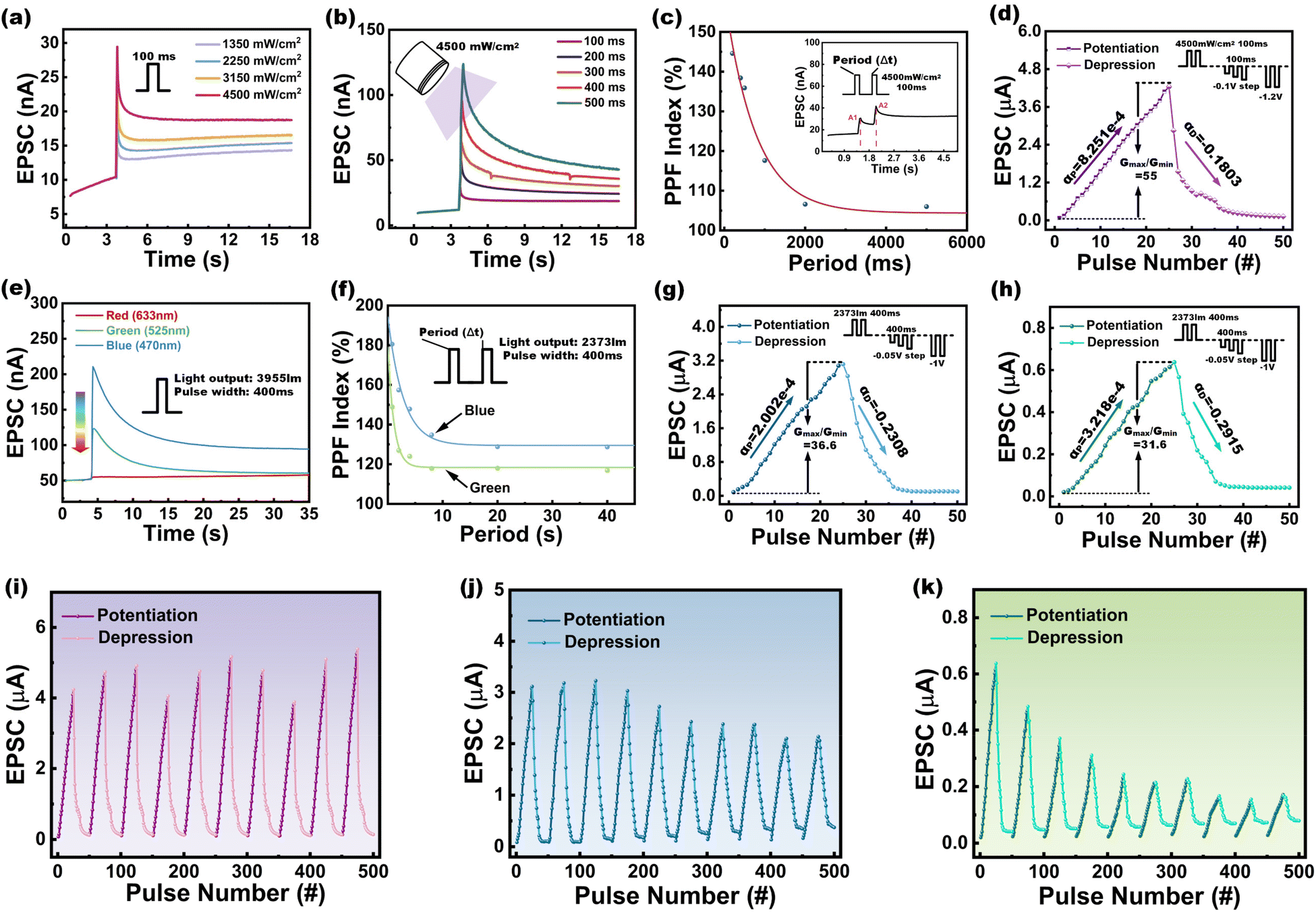 | ||
| Fig. 5 (a) EPSC of the TFT under the stimulation of UV light pulses with a pulse width of 100 ms and various light intensities. (b) The EPSC of the TFT under stimulation of UV light pulses with irradiance of 4500 mW cm−2 and various pulse widths. (c) Paired pulse facilitation (PPF) index (A2/A1) of the TFT under stimulation of 2 consecutive UV light pulses with varying time interval (in terms of period Δt). (d) Potentiation and depression (P/D) of the TFT under stimulation of 25 UV light pulses with irradiance of 4500 mW cm−2 and pulse width of 100 ms, followed by 25 negative gate voltage pulses with the pulse width of 100 ms and pulse amplitude increasing from 0.05 V to 1.2 V with a step of 0.1 V. The base level of all the voltage pulses was fixed at 0.1 V; and the drain voltage (VDS) was fixed at 0.5 V. (e) EPSCs of the TFT under stimulation of visible light pulses with wavelengths of 470, 525 and 633 nm. (f) PPF indexes (A2/A1) of the TFT under stimulation of 2 consecutive blue or green light pulses with light output of 2373 lm, a pulse width of 400 ms and various time intervals. The P/D of the TFT under the stimulation of 25 consecutive pulses of blue light (g) or green light (h) with a light output of 2373 lm and pulse width of 400 ms, followed by 25 negative gate voltage pulses with a pulse width of 400 ms and pulse amplitude increasing from 0.05 V to 1 V with a step of 0.05 V. P/D endurance under 10 repeated cycles of the TFT under the stimulation of UV light pulses (i), blue light pulses (j) and green light pulses (k). | ||
In the visible light experiment, blue, green, and red light with wavelengths of 470 nm, 525 nm, and 633 nm, respectively, were used. Fig. S10† shows the photos of the experimental setup under the illumination of the light with the three wavelengths. The light pulses with a luminous flux of 3955 lm and a pulse width of 400 ms were applied to the TFT. The EPSC signals for the three wavelengths are shown in Fig. 5(e). The EPSC signal became weaker with a longer light wavelength. There was almost no EPSC signal for the red-light illumination. The PPF property of the TFT was characterized by applying 2 consecutive blue or green light pulses with 2373 lm, a pulse width of 400 ms and various time intervals (the period Δt = 0.8, 1.6, 4, 8, 20, and 40 s). Fig. 5(f) shows that the PPF index decreased with the increase of the time interval under the stimulation of 2 consecutive blue or green light pulses. Thereinto, at the shortest time interval (Δt = 0.8 s), the PPF index reached the highest level of 148% under the green light pulses, and 180% under the blue light pulses. Fig. 5(g) and (h) demonstrate the potentiation of the TFT under the stimulation of 25 consecutive blue and green light pulses, respectively; and they also show the depression of the TFT under 25 consecutive negative gate voltage pulses. Some relevant results can be obtained from Fig. 5(g) and (h), as described in the following. The Gmax/Gmin ratios achieved by the stimulation of blue and green light pulses were 36.6 and 31.6, respectively (note that the red-light pulses were not able to produce significant EPSC). The values of αP and αD were obtained from the fittings based on eqn (2). For the P/D inspired by the blue-light pulses/negative gate voltage pulses, αP and αD were 2.002 × 10⁻⁴ and −0.2308 respectively; for the P/D inspired by the green-light pulses/negative gate voltage pulses, they were 3.218 × 10⁻⁴ and −0.2915, respectively. The fittings of the experimental results with eqn (2) are shown in Fig. S9(c)–(f) (ESI†). As can be observed in the figures, with eqn (2) the experimental results could be well described. The asymmetry of the P/D was 0.2306 for the blue light pulses and 0.2913 for the green light pulses. On the other hand, 10 repeated P/D cycles with blue and green light pulses stimulation were conducted to examine the endurance of the P/D. The results are shown in Fig. 5(j) and (k). The Gmax of the potentiation slightly decreased with the P/D cycle under the stimulation of blue light pulses, but deteriorated fast with the P/D cycle under the stimulation of green light pulses. A comparison of P/D characteristics among the different stimulation schemes (including pure electronic pulses and photoelectric pulses) is summarized in Table S3 (ESI†).
As discussed above, both UV and visible light pulses showed the capability to trigger the synaptic behaviors in the TFT. There was an obvious wavelength selectivity of the EPSC signal as shown in Fig. 5(e). Light intensity, pulse width and period showed a high controllability on the EPSC signal of the TFT (see Fig. 5(a)–(c), and (f)). Potentiation was achieved by the stimulation of consecutive photoelectric pulses (i.e., light illumination plus a small positive gate bias); and depression was achieved by the stimulation of the consecutive negative voltage pulses. The photon energy of UV light is larger than the band gap of IGZO (3.2 eV), which could excite electrons from the valence band to the conduction band in IGZO directly and generate electron-hole pairs.13 On the other hand, blue and green light with high light intensity could generate electron–hole pairs in intrinsic sub-gap defect states and excite electrons from the defect states to the conduction band.12 These photon-generated electrons were attracted to the IGZO/TaOx interface under the influence of the positive gate bias and contributed to the production of EPSC. At the light-off state, the positive base level (0.1 V) drove the ion movement in TaOx, which provided an internal electric field inside the dielectric layer to keep attracting electrons to the IGZO/TaOx interface. At the same time, those sub-gap defect states were ionized and turned to be a hole trap center under illumination.12 Photon-generated holes were trapped in the ionized defect states, leading to a photo-gating effect under the collective stimulation of light illumination and positive bias.28,43 The photo-gating effect could contribute to the long-term potentiation in the photoelectric synapse. When a negative bias was applied to the gate terminal, oxygen ions recombined with oxygen vacancies in the TaOx layer, causing the vanish of the internal electric field. At the same time, the negative bias expelled the accumulated electrons away, and the EPSC dropped back to the pristine low level.
4. Conclusions
This article introduced an IGZO TFT with a simple structure showing synaptic behaviors in either the pure electric mode or the photoelectric mode. The high dielectric constant and strong ion conductivity of TaOx collectively contributed to the ultra-low S.S. of the TFT and the achievement of a series of synaptic behaviors. On the other hand, both UV light and visible light sources (blue and green) have successfully inspired the synaptic behaviors as well. All stimulation schemes have inspired a large Gmax/Gmin ratio (>10) and ultra-small non-linearity (<0.5) in the P/D of the TFT. Thereinto, UV-photoelectric pulses have inspired the largest Gmax/Gmin ratio reaching 55; blue-photoelectric pulses have inspired the smallest non-linearity of potentiation as low as 2.002 × 10⁻⁴; negative pulses with a step-increasing amplitude in the pure electronic mode have inspired the smallest non-linearity of depression as low as 0.1501. The simple fabrication process, low thermal budget, and high uniformity of IGZO made the TFT fabricated in this work promising in the applications of large-area neuromorphic computing and vision-based neuromorphic systems.Author contributions
L. Y. B. and J. X. conceptualized the idea and formulated the research goals and aims. L. Y. B. performed the device fabrication, data acquisition, and fitting simulation. J. X. provided the pulse testing probe station. T. S. conducted the XPS experiment and performed the XPS analysis. L. Y. B. wrote the manuscript. C. T. P. supervised the whole project and revised and edited the manuscript. All authors have given approval to the final version of the manuscript.Conflicts of interest
There are no conflicts to declare.Acknowledgements
The research of the project was supported by the Ministry of Education, Singapore, under grant AcRF TIER 1-2020-T1-002-008 (RG144/20). We would also like to thank the staff of the Nanyang NanoFabrication Centre (N2FC) and Facility for Analysis, Characterisation, Testing and Simulation (FACTS) for their assistance in the device fabrication and characterization.References
- L. Abbott and W. Regehr, Nature, 2004, 431, 796 CrossRef CAS PubMed.
- J. Von Neumann, IEEE Annals of the History of Computing, 1993, vol. 15, p. 27 Search PubMed.
- Q. Wan, M. T. Sharbati, J. R. Erickson, Y. Du and F. Xiong, Adv. Mater. Technol., 2019, 4, 190037 Search PubMed.
- V. M. Ho, J.-A. Lee and K. C. Martin, Science, 2011, 334, 623 CrossRef CAS PubMed.
- R. S. Zucker and W. G. Regehr, Annu. Rev. Physiol., 2002, 64, 355 CrossRef CAS PubMed.
- H. Han, H. Yu, H. Wei, J. Gong and W. Xu, Small, 2019, 15, 1900695 CrossRef PubMed.
- T. V. P. Bliss and S. F. Cooke, Clinics, 2011, 66, 3 CrossRef PubMed.
- T. Kamiya, K. Nomura and H. Hosono, Appl. Phys. Lett., 2010, 96, 122103 CrossRef.
- T. Kamiya, K. Nomura and H. Hosono, J. Disp. Technol., 2009, 5, 273 CAS.
- T. Kamiya and H. Hosono, NPG Asia Mater., 2010, 2, 15 CrossRef.
- A. Chen and M.-R. Lin, IEEE International Reliability Physics Symposium (IRPS), Monterey, CA, USA, 2011 Search PubMed.
- H. Oh, S.-M. Yoon, M. K. Ryu, C.-S. Hwang, S. Yang and S.-H. K. Park, Appl. Phys. Lett., 2010, 97, 183502 CrossRef.
- M. Mativenga, F. Haque, M. M. Billah and J. G. Um, Sci. Rep., 2021, 11, 14618 CrossRef CAS PubMed.
- H. K. Li, T. P. Chen, P. Liu, S. G. Hu, Y. Liu, Q. Zhang and P. S. Lee, J. Appl. Phys., 2016, 119, 244505 CrossRef.
- Y. Kaneko, Y. Nishitani and M. Ueda, IEEE Trans. Electron Devices, 2014, 61, 2827 CAS.
- M.-K. Kim and J.-S. Lee, Nano Lett., 2019, 19, 2044 CrossRef CAS PubMed.
- N. Duan, Y. Li, H.-C. Chiang, J. Chen, W.-Q. Pan, Y.-X. Zhou, Y.-C. Chien, Y.-H. He, K.-H. Xue, G. Liu, T.-C. Chang and X.-S. Miao, Nanoscale, 2019, 11, 17590 RSC.
- J. Sun, S. Oh, Y. Choi, S. Seo, M. J. Oh, M. Lee, W. B. Lee, P. J. Yoo, J. H. Cho and J.-H. Park, Adv. Funct. Mater., 2018, 28, 1804397 CrossRef.
- W. Yang and R. Jiang, Appl. Phys. Lett., 2019, 115, 022902 CrossRef.
- Y. Yang, Y. He, S. Nie, Y. Shi and Q. Wan, IEEE Electron Device Lett., 2018, 39, 897 CAS.
- L. Zhu, Y. He, C. Chen, Y. Zhu, Y. Shi and Q. Wan, IEEE Trans. Electron Devices, 2021, 68, 1659 CAS.
- Y. Hayakawa, A. Himeno, R. Yasuhara, W. Boullart, E. Vecchio, T. Vandeweyer, T. Witters, D. Crotti, M. Jurczak, S. Fujii, S. Ito, Y. Kawashima, Y. Ikeda, A. Kawahara, K. Kawai, Z. Wei, S. Muraoka, K. Shimakawa, T. Mikawa and S. Yoneda, IEEE Symposium on VLSI Circuits (VLSI Circuits), Kyoto, Japan, 2015 Search PubMed.
- W. Kim, D. J. Wouters, R. Waser and V. Rana, IEEE International Symposium on Circuits and Systems (ISCAS), Daegu, Korea, 2021 Search PubMed.
- S. R. Lee, Y.-B. Kim, M. Chang, K. M. Kim, C. B. Lee, J. H. Hur, G.-S. Park, D. Lee, M.-J. Lee, C. J. Kim, U.-I. Chung, I.-K. Yoo and K. Kim, IEEE Symposium on VLSI Technology (VLSIT), Honolulu, HI, USA, 2012 Search PubMed.
- P. B. Pillai and M. M. D. Souza, ACS Appl. Mater. Interfaces, 2017, 9, 1609 CrossRef PubMed.
- K. Beom, P. Yang, D. Park, H. J. Kim, H. H. Lee, C. J. Kang and T.-S. Yoon, Nanotechnology, 2018, 30, 025203 CrossRef PubMed.
- Z. Zhou, Y. Pei, J. Zhao, G. Fu and X. Yan, Appl. Phys. Lett., 2021, 118, 191103 CrossRef CAS.
- G. Feng, J. Jiang, Y. Li, D. Xie, B. Tian and Q. Wan, Adv. Funct. Mater., 2021, 31, 2104327 CrossRef CAS.
- Neuronal synaptic docking, https://699pic.com/tupian-401565205.html, (accessed 12 June 2021).
- Y. J. Chung, J. H. Kim, U. K. Kim, M. Ryu, S. Y. Lee and C. S. Hwang, Electrochem. Solid-State Lett., 2011, 14, H300 CrossRef CAS.
- E. Carlos, R. Branquinho, A. Kiazadeh, J. Martins, P. Barquinha, R. Martins and E. Fortunato, ACS Appl. Mater. Interfaces, 2017, 9, 40428 CrossRef CAS PubMed.
- J.-W. Jo, K.-H. Kim, J. Kim, S. G. Ban, Y.-H. Kim and S. K. Park, ACS Appl. Mater. Interfaces, 2018, 10, 2679 CrossRef CAS PubMed.
- L. Li, Y. Shao, X. Wang, X. Wu, W.-J. Liu, D. W. Zhang and S.-J. Ding, IEEE Trans. Electron Devices, 2020, 67, 105 CAS.
- S.-H. Kim and W.-J. Cho, Int. J. Mol. Sci., 2021, 22, 1344 CrossRef CAS PubMed.
- P. Yang, H. J. Kim, H. Zheng, G. W. Beom, J.-S. Park, C. J. Kang and T.-S. Yoon, Nanotechnology, 2017, 28, 225201 CrossRef PubMed.
- S. Choi, I. Chae, J. Park, Y. Seo, C. I. Ryoo, D. M. Kim, S.-J. Choi, D.-W. Park and D. H. Kim, IEEE Electron Device Lett., 2020, 41, 1778 CAS.
- S. U. Sharath, M. J. Joseph, S. Vogel, E. Hildebrandt, P. Komissinskiy, J. Kurian, T. Schroeder and L. Alff, Appl. Phys. Lett., 2016, 109, 173503 CrossRef.
- Z. Wang, M. Yin, T. Zhang, Y. Cai, Y. Wang, Y. Yang and R. Huang, Nanoscale, 2016, 8, 14015 RSC.
- S. Yu, P.-Y. Chen, Y. Cao, L. Xia, Y. Wang and H. Wu, IEEE International Electron Devices Meeting (IEDM), Washington, DC, USA, 2015 Search PubMed.
- P.-Y. Chen, X. Peng and S. Yu, IEEE Trans. Comput.-Aided Des. Integr. Circuits Syst., 2018, 37, 3067 Search PubMed.
- M. Jerry, P.-Y. Chen, J. Zhang, P. Sharma, K. Ni, S. Yu and S. Datta, IEEE International Electron Devices Meeting (IEDM), San Francisco, CA, USA, 2017 Search PubMed.
- J. Chen, C.-Y. Lin, Y. Li, C. Qin, K. Lu, J.-M. Wang, C.-K. Chen, Y.-H. He, T.-C. Chang, S. M. Sze and X.-S. Miao, IEEE Electron Device Lett., 2019, 40, 542 CAS.
- Y. Hou, L. Wang, X. Zou, D. Wan, C. Liu, G. Li, X. Liu, Y. Liu, C. Jiang, J. C. Ho and L. Liao, Small, 2020, 16, 1905609 CrossRef CAS PubMed.
Footnote |
| † Electronic supplementary information (ESI) available. See DOI: https://doi.org/10.1039/d2nr02136f |
| This journal is © The Royal Society of Chemistry 2022 |