
 Open Access Article
 This Open Access Article is licensed under a Creative Commons Attribution-Non Commercial 3.0 Unported Licence
Observation of a Yu-Shiba-Rusinov state originating from the magnetic moment in a curved monolayer island of 1T-phase NbSe2![[thin space (1/6-em)]](https://www.rsc.org/images/entities/h2_char_2009.gif) †
†
Hossain
Mohammad Ikram
*ab,
Ara
Ferdous
 ac,
Shahed
Syed Mohammad Fakruddin
ac,
Zhipeng
Wang
ab and
Tadahiro
Komeda
*c
ac,
Shahed
Syed Mohammad Fakruddin
ac,
Zhipeng
Wang
ab and
Tadahiro
Komeda
*c
aDepartment of Chemistry, Graduate School of Science, Tohoku University, 6-3, Aramaki Aza-Aoba, Aoba-ku, Sendai 980-8578, Japan
bCenter for Spintronics Research Network, Tohoku University, 2-1-1 Katahira, Aoba-ku, Sendai 980-8577, Japan
cInstitute of Multidisciplinary Research for Advanced Materials (IMRAM, Tagen), Tohoku University, 2-1-1, Katahira, Aoba-Ku, Sendai 980-0877, Japan. E-mail: tadahiro.komeda.a1@tohoku.ac.jp
First published on 6th June 2022
Abstract
We report the finding of a 1T phase island of NbSe2 on a cleaved surface and its magnetic properties. Tunneling spectroscopy at 400 mK shows robust peaks in the superconducting gap, which we assign to the Yu-Shiba-Rusinov (YSR) state originating from the magnetic moment placed in the superconducting state. The YSR peak appears on a specific position of an island of the 1T phase, not on the surrounding 2H phase area, and shows an anisotropic decay behavior. In addition, we found a close relationship between the enhancement of the YSR peak and the local curvature of the film. We assign the origin of the magnetic moment to the curvature of the 1T phase island, which can form a magnetic moment through a rotation of the wave function by a robust spin–orbit coupling, as indicated by a recent theoretical study.
An atomic-scale thin layer of transition metal dichalcogenides (TMDs) attracts attention as a material for electronic applications. To apply TMDs to advanced devices that use the spin degree of freedom, control of the magnetization in the nanoscale region is critical. Such modifications in a limited spatial area might be possible using structural changes that appear in different crystal phases or strain accumulation utilizing the mechanical flexibility of the film. Such engineering started with a graphene layer,1–3 but similar research is actively conducted on TMD materials. Significantly, many reports studied the control of the magnetism of TMDs in a confined region.4–12
At the same time, it is required to develop an instrument to prove the local magnetism with high sensitivity. For this purpose, we have to search for a spectroscopic feature sensitive to a local field. The use of the spectroscopic characteristics of the superconducting state can provide a high sensitivity to the magnetic field.13 When a magnetic impurity is placed on the superconductor's surface, the magnetic interaction breaks the Cooper pair. It forms a bound state inside the superconductor gap, called the Yu-Shiba-Rusitov (YSR) state. The energy position of the YSR state is sensitive to the magnetic moment and the exchange interaction with the superconductor. Thus, we might utilize the YSR feature as a sensitive local magnetic-field sensor.14
NbSe2 is a TMD material which shows superconductivity (SC),15 for which two types of structure, 2H and 1T, are reported. Both show a charge density wave (CDW) in scanning tunneling microscopy (STM) images,16–18 which is evidence of the strong electron interaction.19,20 Zhou and coworkers theoretically studied the magnetism for the film of NbSe2.21
This report studies a 1T-phase island with a √13 × √13 R13.9° reconstructed surface,16,18 which appears on the cleaved surface. The size is ∼50 nm and is elevated from the surrounding 2H area by the height of the unit cell of NbSe2. This island looks like a domain epitaxially grown on the 2H substrate but created in the cleavage process. In scanning tunneling spectroscopy (STS) under sub 1 K conditions, we found robust features in the superconductor gap, separated from the gap edge. We found the in-gap peaks only in the 1T island at a specific position along a symmetry line and not detected on the 2H area. This in-gap state showed intriguing position dependence for intensity and energy positions, which we assign to the YSR state, originated from a magnetic impurity.14 We assign the origin of magnetic moment to the curvature of the NbSe2 layer of the 1T island.
Results and discussion
NbSe2 is composed of stacked unit layers. The unit layer contains three layers of Se, Nb, and Se. The 2H and 1T phases of NbSe2 possess different configurations of the unit layer, as illustrated in Fig. 1(a). The triangles of the Se atoms of the upper and lower Se layers point in the same direction in the former case but rotate by 180° in the latter. The stacking of the unit layers is through the van der Waals force between them, and the cleavage exposes the Se layer. Fig. 1(b) shows the stacking of the two-unit layers of 2H with a periodicity of 6.8 Å. The 2H phase is more stable than the 1T phase, the latter of which is not observed in the bulk phase. The topmost surface of the cleaved NbSe2 is the 2H unit with a high probability. | ||
| Fig. 1 (a) A schematic model of NbSe2 in 2H and 1T phases. (b) Side view of 2H bulk with monolayer height. (c) A STM image of the boundary of 2H and 1T phases. | ||
We illustrate the STM image of the NbSe2 surface obtained in this experiment in Fig. 1(c). The sample was cleaved at room temperature and cooled to a temperature of 400 mK for observation. We see the atomic image of Se atoms with a periodicity of 3.4 Å. In addition, we identify the superstructure of 3 × 3, which was previously reported and originated from the CDW structure of the 2H phase.17,22,23
At the same time, we frequently observed the 1T phase domain on the freshly cleaved NbSe2 surface, an example of which is shown in Fig. 2(a). We assign it to the 1T phase domain judging from the characteristic reconstructed superstructure with a periodicity of √13 × √13 R13.9°.16,18
 | ||
| Fig. 2 A topographic image of the 1T island (bright area with the reconstruction of √13 × √13 R13.9°) on top of the 2H substrate (dark surrounding) (a), its height profile at the edge (b), and the magnified image at the perimeter (c). (d) High-resolution image of the interface region. Se atoms are visible on the right side of the 2H part. Symmetry lines connecting Se atoms and the star of David are illustrated in white. (e) A model of the 2H substrate (upper) and 1T (lower, one layer higher than 2H). Unit vectors of 1 × 1 of 2H and√13 × √13 R13.9° are expressed by a, b and s, and t, respectively. A model of the star of David connecting the Nb atoms is illustrated. (f) Comparison of the STS obtained at 1T and 2H areas. Vertical lines are the eye-guide of the superconductor gap of the 2H phase. | ||
The island is elevated from the surrounding area by 6.8 Å, as illustrated in Fig. 2(b) by the cross-sectional height profile, corresponding to the periodicity of the stacking of unit layers. The surrounding flat area shows a 3 × 3 reconstructed CDW characteristic of the 2H phase and is similar to Fig. 1(c).
Although the 2H phase is more stable in energy than the 1T phase, the energy difference is relatively small. Thus, previous reports showed the creation of the 1T phase with some outer stimulations such as strain,24,25 heat,18 and the intercalation of metal atoms.26,27 The cleaving process can cause a transfer from the 2H to 1T phase.
Even though the interaction of the STM tip and the NbSe2 surface can cause the transition from 2H to 1T by the tunneling current,28 or the electric field,29 we judged that this is not the case for the 1T island of Fig. 2(a) based on the height difference from the surroundings. Bischoff and coworkers showed a high-resolution image of the boundary between the 2H phase surface and the reconstructed 1T phase domain created by the tunneling current. The atomically resolved interface image shows a negligible height difference. We confirmed the slight height difference between these phases with our set-up, and the results of the topographic STM image analysis and the height profile are presented in the first section of the ESI.† Thus, the STM effect does not induce the elevated 1T phase island of Fig. 2(a). Instead, the 1T island is formed in the cleaving process.
The magnified images of the island surface with the √13 × √13 R13.9° reconstruction are shown in Fig. 2(c) with a further zoom-in image in 2(d). The Se atoms are visible, and two white lines connecting the Se atom positions are indicated in Fig. 2(d).
We show a crystallographic model of the 1T island with the 13 × √13 R13.9° reconstruction and the substrate 1 × 1 2H surface in Fig. 2(e). In the upper part, we illustrate two vectors of a and b corresponding to the unit vectors of the 1 × 1 lattice of the Se atom (length 3.4A). In the 1T region, star-like polygons represent the superstructure, often referred to as the star of David. The unit vectors of s and t with a length of √13 nnd (nnd is the Se–Se distance in the close-packed direction) describe the unit cell of the superstructure. The vector t is tilted from the vector b by θ (= 13.9°).
It is important to note that the center of the star of David is located on the top of the Nb atom and shifted from the symmetry line connecting the Se positions. We examine the alignment in the experimental image in Fig. 2(d). We superimposed two symmetry lines in white connecting the Se atoms. We also show the star of David by white polygons on the bright area of the reconstructed surface. The center of the star of David, shown as white dots, is between the two white lines, reproducing well the model of Fig. 2(e). The agreement with the model demonstrates that the 1T island has a good crystallographic relationship with the underlying 2H substrate.
The difference in the physical properties of the 1T island from the surrounding 2H phases appears in the superconductor gap. We compared the STS spectra obtained by positioning the STM tip on the domains of the 2H and 1T phases in Fig. 2(f). Both spectra show the superconductor gap flanked by high conductance peaks corresponding to the quasi-particle excitation. We illustrate two vertical lines as a guide to the eye, and we notice that the gap is smaller for the 1T phase than for the 2H phase. These two spectra were obtained with the same tip. We can compare the energy positions without calibrating the tip-effect due to the coating of the tip surface with the superconductor materials.
We show another example of a similar 1T-phase island in Fig. 3(a). The 3D-like representation shown in Fig. 3(b) illustrates the darker area in Fig. 3(a) in pink color and the higher island in blue color, indicating that both areas are flat. The STM topographic image of the island is as smooth as any part of the 2H-phase surface, and we consider that the island is homogeneous.
 | ||
| Fig. 3 (a) An example of a 1T island on top of the 2H substrate. A, B, and C mark the undulation of the film. (b) 3D illustration of (a). (c) A magnified image of √13 × √13 R13.9° reconstructions. (d) The STS spectrum obtained on the 1T island. | ||
However, we can observe a slight undulation in the topographic image of Fig. 3(a). Along the line connecting A and C, there is a belt where the surface is lower than the surrounding area, whose height difference is ∼20 pm. A–B and A–C are along the unit vectors of the reconstructed surface (s and t of Fig. 2(e)), and the B–C is perpendicular to that direction.
Thus, the center of the triangle resembles a low-height dome with a triangle perimeter. Though a similar dome formation was reported for the graphene layer, the reported height is 5 Å, much higher than observed in this report.30 The superstructures are disturbed around A and B, and dislocated alignment of the bright areas of the superstructure appears.
When we use a lower tunneling voltage (Vs = −50 mV), bright lines spread from each bright spot connecting the neighboring sites (see Fig. 2(d)).31,32 In addition, to confirm that the island has the same electronic structure reported in previous reports, we examine the CDW gap. The STS obtained for the energy range of (−10 mV, 10 mV) is illustrated in Fig. 3(d). There appear characteristic peaks at symmetric positions about the Fermi level and separated by 2Δ, together with the SC gap already shown in Fig. 2(f). The 2Δ separated peaks should be the CDW gap. We see the wide gap separated 2Δ ∼7 mV and the narrow SC gap. The size of the CDW gap is similar to the one reported previously, and we believe that we have confirmed the CDW state of this film.33 This is clear evidence that the electronic structure of the CDW phase appears on the island.
The area around the dome provides a peculiar electronic structure, which we show by tunneling spectroscopy. Fig. 4(a) is a magnified image of Fig. 3(a). Point B indicates the identical position in both images. We obtained dI/dV spectra in the energy range of a few meV around the Fermi level using the lock-in amplifier technique superimposing the modulation voltage (Vrms = 50 μV). In most of the 1T islands, we obtained the spectrum shown as I in Fig. 4(b), which is composed of the SC gap flanked by the quasi-particle (QP) peaks. Hereafter the STS spectra are numerically fitted by dividing them into components of the SC gap and Lorentzian peaks. The detail of the fitting is presented in the ESI.†
 | ||
| Fig. 4 (a) A magnified image of Fig. 3(a) around the position ×. (b) STS spectra of SC gap and QP peaks, I, and the sharp in-gap state, II, observed at ×. (c) A comparison between the QP state and the in-gap state was obtained at several positions. (d) Measurement points of STS for the site-specific STS superimposed on the area around × of (a). (e) 3D presentation of the STS spectra measured at positions of (d). For the spectrum representation, see the main text. | ||
When we positioned the STM tip at mark × in Fig. 4(a), a new dI/dV feature appeared inside the SC gap, whose shape is shown as II in Fig. 4(b). The peak has a narrow width and an intensity one order of magnitude higher than the QP peaks, the latter of which is almost invisible compared to the new features. Spectrum II in Fig. 4(b) has a much larger intensity than spectrum I. Thus, it might seem that the QP peaks do not appear at around point ×. However, the QP is not visible due to the intensity issue, and we show the spectrum obtained at positions slightly separated from × in Fig. 4(c). The energy positions of the QP, visible in the top spectrum, are on the vertical lines. The newly appeared peaks are visible in the middle and bottom plots, in which the QP features are also visual.
We show the position dependence of the STS spectra near the Fermi level. STS spectra were accumulated around point × and along four symmetry lines indicated by A to D in Fig. 4(d), with sequential numbers for each line. We plotted the dI/dV in a 3D manner in Fig. 4(e). Each dI/dV is centered at the measurement position of the superimposed topographic image. The energy axis is placed in the plane and perpendicular to the symmetry line (A–D). The dI/dV amplitude is shown as the z-height, whose difference is enhanced with the coloring of the color table.
The most substantial in-gap state appears at the center, point ×. In the region between × and A12, the high-intensity in-gap peaks appear at all points where A12 is separated by 1.8 nm from ×. Similarly, on line D, enhanced in-gap peaks appear at the positions from D5 to D14, the latter of which is 2.6 nm separated from point ×. Meanwhile, the variation of the spectra obtained along the lines of B and C shows a monotonic decay from the strong in-gap peak at × with the distance, and the spectrum shape returns to the standard QP shape.
We show more details of the variation of the STS spectra along the four symmetry lines in Fig. 5. The fitting of the in-gap state and the obtained parameters are shown in the ESI.†Fig. 5(a) shows the variation along with line A. The variation is also illustrated in the color mapping in Fig. 5(b), in which the x-axis is the energy position, and the y-axis is the measurement position.
 | ||
| Fig. 5 (a), (c) and (d) STS spectra obtained at points along lines A, D, and B defined in Fig. 4, respectively. The center position × is shared by lines A–D, but spectra at the position were measured for each series. The thin vertical lines are the energy positions of features QP, Y1, and Y2 (see the main text). (b) A color map of QP, Y1, and Y2 features. Bright (dark) color corresponds to the high intensity of the STS spectrum. The axis of x and y are the energy and position along with line A, respectively. (e) and (f) Bubble plots converted STS spectra along with lines A–D with a superimposed topographic image for the measurement point. The diameter and the color represent the intensity and the energy position of the peak of each spectrum. | ||
At A1 (the end of the horizontal line), we see the SC gap and the flanking QP peaks, the latter of which is indicated by the vertical lines at ±1.1 meV. Between A6 and A12, straddling the center ×, we see the presence of in-gap peaks. These features can be grouped as Y1 at ±0.5 meV and Y2 at ±0.9 meV, at which we draw the vertical lines.
Though feature Y2 is close to the gap edge, we can easily differentiate it from the QP. Y2 is not visible at A1 but appears at A3. It becomes gradually enhanced from A3 to A7 while remaining at the same energy position. From A7 to A8 (identical with ×), the intensity of feature Y1 shows a rapid increase and it dominates at ×. From A8 to A12, feature Y1 gradually shifts its energy away from the Fermi level while the intensity decreases.
Fig. 5(c) illustrates the STS variation along with line D, in which we show vertical lines at the identical energy positions as in Fig. 5(a). The in-gap features show a complex change. If we start from D1 and trace the measurement points downward, feature Y1 becomes visible at D5 (separated 1.86 nm from ×), and is dominant at ×. The intensity of Y1 decreases drastically at D8, but Y2 becomes enhanced, which continues to be prominent up to D14 (separated 5.0 nm from ×).
However, the intensity variations along lines B and C show a rapid and monotonic decay from the center ×. The variation along with line B shown in Fig. 5(d) indicates that the dominant feature Y1 at the center × decreases its intensity drastically at B5 and B7, separated by 0.6 nm from the center ×, and disappears afterward (see the ESI† for the plots along with line C).
As illustrated above, the peak intensity and the energy positions of the in-gap peaks change in a complex manner. We demonstrate the change using a bubble plot for the energy region of Y1 and Y2 in Fig. 5(e) and (f), respectively. The diameter and color of the circles correspond to the intensity and energy positions of the YSR component, respectively. The plots visualize that both the energy and intensity of the in-gap state strongly depend on the crystallographic directions; Y1 features on the right-hand side of line A, while Y2 on the lower part of D and left part of A.
The scattering of electrons by imperfections of the superconductor crystal can form electronic states inside the superconducting gap. If non-magnetic impurities cause the scattering, the newly formed bound state is close to the SC gap edge and the QP peaks.34 When the impurity is magnetic, the bound state appears separated from the SC gap edge. The magnetic field suppresses the superconductivity, and the enhanced scattering makes a large splitting of the bound states. When we treat the magnetic impurity as the classical spin, we expect the Yu-Shiba-Rusikov (YSR) state to appear.14
The in-gap state shown in this work is well separated from the SC gap edges and should be assigned to the YSR peaks originating from the interaction with a magnetic moment. We can express the energy position of the YSR state with the parameters of the exchange interaction. Flatté and coworkers demonstrated numerical estimation of the YSR energies,35 and more recent reports showed that the energy positions of the YSR states are sensitive to the chemical environment of the magnetic impurity.13,36 The energy positions can be expressed with the following formula for pure magnetic spherical symmetric exchange interaction potential;

Thus the bound state approaches the Fermi level with the increase of J in the initial stage. The energy position of the Y1 state shown in Fig. 5(b) approaches the Fermi level when the place gets closer to ×. The energy shift implies that the magnetic moment increases around the position ×.
However, bulk NbSe2 is non-magnetic, and we have to figure out what makes the magnetic moment. One possible source of magnetic impurity is the intercalated magnetic metal in the subsurface position. The layered structure of TMD can make the intercalation of metal atoms easier. A recent work by Ménard and coworkers detected the YSR state formed by an Fe atom impurity intercalated in the subsurface of the 2H-NbSe2 sample.37 They found that the YSR peak decays slowly in the lateral direction in an isotropic manner with a decay length of 10 nm. Interestingly, the decay length observed for the magnetic adatom is on an atomic scale for a magnetic metal atom adsorbed on the superconductor Pb surface.38,39 The result shows a short decay of the atomic scale.
The intercalated and adatom magnetic impurity behaviors are quite different from what we found in this experiment, in which the distribution of the energy position and the intensity of the YSR peaks are sensitive to the crystallographic direction. If the intercalated metal atoms form a chain or a cluster, the YSR features might be distributed by tracing the area. However, considering the purity of NbSe2 and the concentration of a possible magnetic metal atom, it is unlikely they make an assembly in a line.
Since the enhanced YSR feature appears in the neighborhood of the dome shown in Fig. 3(a), we consider a model in which the surface curvature is responsible for the appearance of the YSR feature. In the previous studies of graphene, we see many examples in which the curvature in the graphene layer generates a wide variety of effective magnetic fields.40,41 The phenomenon is accounted for by examining the Dirac equation in curved space that shows a gauge field similar to the electromagnetic field. Experimentally, the dome of graphene using STM and higher than 300 T magnetic field was detected.30
Ochoa and coworkers reported an electromagnetic effect caused by the corrugation of the TMD film. The mechanism for the appearance of the magnetic moment is different from that for the graphene layers.42 In the presence of corrugations, the sizeable spin–orbit coupling rotates the wave function in the spinor basis, which may engender a gauge field. Although the mechanism for the appearance of the magnetic moment is different from the graphene case, the generation of the magnetic field is suggested.
We examine the curvature of the NbSe2 layer as a part of the origin of the magnetic moment. In Fig. 6(a), we display the topo-image using the multi-color representation. As already discussed in Fig. 3(a), there runs a shallow trough parallel to the symmetry direction of the CDW structure. The trough is in the area with orange-bordered circles. The long white lines correspond to the lines discussed in Fig. 4 and 5.
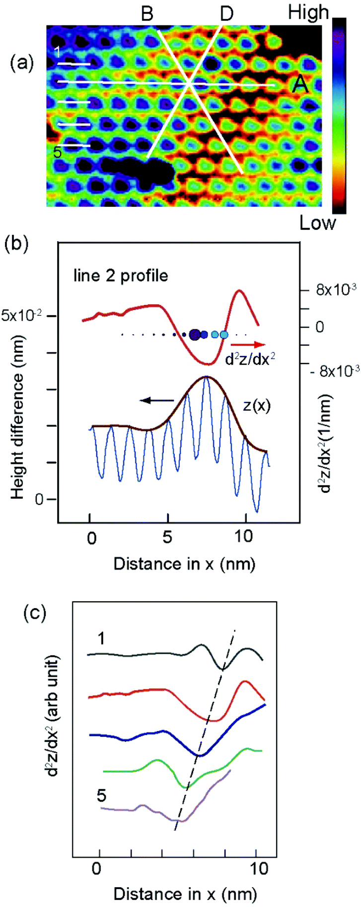 | ||
| Fig. 6 (a) A topographic image for the STS measurement points of Fig. 4 and 5, with the color code shown on the right-hand side. (b) Cross-sectional height profile along the line 2 of (a) in the blue line, and its envelope function z(x) in brown color. The curve of d2z(x)/dx2 is shown by red lines where the plot of Fig. 5(f) is superimposed. (c) Second derivative of the height profile along the lines of 1–5 of (a) obtained with the method of (b). The dotted line indicates the eye-guide of the minimum positions of the curves. | ||
We first analyzed the height profile along with the corrugated positions of the CDW superstructure in the horizontal direction. The lines are sequentially named from 1 to 5, as indicated in Fig. 6(a), starting from the same lateral position. Line 2 coincides with line A in Fig. 4(d). The blue line in Fig. 6(b) shows the height profile, which illustrates the groove of the CDW electronic structure. To examine the undulation of the layer numerically, we first fit the curve with an envelope function plotted by the brown line of Fig. 6(b). In the right-hand end, we see a lower trough part. The envelope curve shows the highest position close to × defined in Fig. 4 and 5. We calculated the second derivative of the envelope function in the upper part of Fig. 6(b) to estimate the curvature numerically. Due to the convex profile, the second derivative shows a negative value at around ×. We superimpose the bubble plot on this second derivative curve, which is already shown in Fig. 5(e). Interestingly, the robust YSR features appear for the regions where the second derivative shows large negative values.
In addition, we assembled the second-derivative curves for the lines of 1–5 in Fig. 6(c). All the curves show clear minima, whose trace is shown by the dotted line. This line coincides with line D of Fig. 4(d) (also shown in Fig. 6(a)). The structural analysis explains why the strong YSR peak continuously appears along D, as illustrated in the bubble plot of Fig. 5(f). In other words, the STS spectra of D7–D13 are obtained at the positions of the immense curvature, which rationalizes that the spectra of D7–D13 give high YSR intensity.
The position of the large curvature of the island is concentrated along line D. Thus, along line B, the curvature shows a quick decrease from the center ×, which makes the fast and straightforward decay of the YSR peak, as shown in Fig. 5(e) and (f).
To demonstrate the 1T island and YSR states that can be observed in many places on the cleaved surface, we show another example in the ESI.† The results show a similar correlation between the film curvature and the enhancement of the YSR peak.
As a control experiment, we show the case for the 1T island without the curvature, which is shown in Fig. 7(a), comparing to the curved island in Fig. 7(b). The line profile along line 1 of Fig. 7(a) (line 2 of 7(b)) is illustrated in Fig. 7(c) (in 7(d)). The absence of the curvature along line 1 is obvious if we compare the two curves of Fig. 7(c). The STS taken along line 1 of Fig. 7(a) is monotonic and contains only the QP peaks, which we illustrate in the plots a and b of Fig. 7(d) for representing spectra. The spectrum shows a large contrast with that obtained at the curved position of d, specified in Fig. 7(c).
 | ||
| Fig. 7 A reconstructed surface of the 1T phase island on a 2H substrate without curvature (a) and with curvature (b). (c) The line profile along line 1 (line 2) of (a) (of (b)). (d) STS spectra at the points specified in (c). Along line 1, the STS is monotonic as represented by spectra a and b. | ||
We should mention the behavior of the YSR states on the 2H island. Even though we scanned the surface of the 2H phase area, no YSR features appeared. We consider the most plausible scenario for finding the YSR peaks at the curved area of the 1T film (and not for the 2H phase) like the following. First, the 1T monolayer film tends to possess magnetization. Theoretical studies demonstrated the magnetization for the 1T phase monolayer film in the vacuum. Calandra and coworkers predict that the 1T phase monolayer film with a √13 × √13 R13.9° reconstructed structure harbors a magnetic moment of spin 1/2 after taking the Hubbard U method. The hybridization between the dz2−r2 of the Nb 4d orbital and the Se 4p orbital is reduced in this structure, suppressing the covalent bonding between the two and recovering the 4d magnetic moment.32 Experimentally, the magnetization of the 1T phase film was reported for the NbSe2 monolayer grown on the graphene substrate. Liu and coworkers detected the Kondo resonance.43 In addition, recent studies reported similar phenomena.44,45 Even though the structures for these reports are different from our case where the 1T phase film exists on the 2H substrate, we speculate that the reason why we do not observe the enhanced YSR feature in the 2H film should be related to the tendency of the 1T phase film for the magnetization.
However, the reconstructed 1T monolayer film on the 2H substrate does not have the magnetization to be detected by the YSR states, and it requires the help of the curvature. The model can explain why the YSR peak appeared in a specific position with high curvature in the 1T film. As we stated above, the theoretical study demonstrated that the curvature of the TMD film tends to cause magnetization.42 We consider that this is the reason why the YSR feature is only detected at the curved area of the 1T film. However, further theoretical examination is required.
In the last section, we consider a mechanism of curvature formation, focusing on the difference of the lattice constant of the two phases: the one for the 1T phase is 1% larger than that of the 2H phase deduced from DFT calculation.46 The 1T layer island we discussed in this study is isolated. It might be easier for the layer to form a curved surface to release the stress accumulated by the lattice-constant difference compared to the case where the 2H area surrounds the 1T phase in the same plane. The model might rationalize the formation of the curved 1T island. The detailed analysis is shown in Fig. S3 of the ESI.†
As we already discussed, the 1T domain prepared by STM manipulation, demonstrated by Bischoff et al.,16 is different from the 1T island we discussed in this manuscript, while the 2H layer surrounds the 1T domain in Bischoff's domain, the 1T island we discussed is isolated, and the entire island is in the 1T phase. Liu and coworkers examined the electronic and magnetic properties of the Bischoff type 1T domain.43 They discussed the effect of the heterointerface of the 2H-1T phases, which changes the electronic structure from the free-standing 1T layer and possibly modifies the inter star of David interaction. For the 1T island of this manuscript, the absence of the surrounding 2H phase from the surrounding should change their electronic/magnetic properties. Further experimental and theoretical investigation into the effect of these differences is required.
Conclusion
We reported the 1T phase island of NbSe2, which is isolated and elevated 6.8 Å from the surrounding 2H area on a cleaved surface from the bulk NbSe2. STM images obtained at 400 mK show the √13 × √13 R13.9° reconstruction with the star of David, which shows the expected registry with the 2H substrate. The STS shows robust peaks in the superconducting gap, which we assign to the YSR state originating from the magnetic moment placed in the NbSe2 SC state. The YSR peak appears on a specific position of the 1T island, not on the surrounding 2H area. It shows an anisotropic decay behavior from a center position at which the YSR peak shows the maximum separation from the SC-gap edges with significant intensity. In addition, we found a close relationship between the enhancement of the YSR peak and the local curvature of the film. We assign the origin of magnetic moment to the curvature of the 1T phase island. Combined with the tendency of the 1T phase layer for magnetism, the curvature of the 1T film can cause local magnetization, which can be applied for the nanoscale control of the magnetic field.Experimental
Single crystal NbSe2 was purchased from HQ Graphene (Netherlands). The 3 × 3 mm2 flake was fixed on the sample folder while the surface was covered with glue in which a short W wire was attached. After inserting the sample into the ultra-high vacuum (UHV) chamber, the W wire was mechanically pushed to make the NbSe2 surface cleaved. The STM head and cooling system were constructed based on a commercially available instrument (USM-1300, Unisoku, Japan), with a 3He refrigerator which achieves a temperature of 400 mK at the sample and STM tip. They system is operated by 3He condensation using a 1 K pot and pumping using a charcoal sorption pump.The STM control system is equipped with a current-amplifier (DLPCA 200, FEMTO) operated with the gain of 109. The dI/dV was obtained by using a lock-in amplifier with the modulation voltage Vrms = 50 μV.
Conflicts of interest
There are no conflicts to declare.Notes and references
- S.-M. Choi, S.-H. Jhi and Y.-W. Son, Phys. Rev. B: Condens. Matter Mater. Phys., 2010, 81, 081407 CrossRef.
- D. W. Boukhvalov and M. I. Katsnelson, J. Phys. Chem. C, 2009, 113, 14176–14178 CrossRef CAS.
- V. M. Pereira and A. H. Castro Neto, Phys. Rev. Lett., 2009, 103, 046801 CrossRef PubMed.
- Y. Xu, X. Liu and W. Guo, Nanoscale, 2014, 6, 12929–12933 RSC.
- P. Manchanda, V. Sharma, H. Yu, D. J. Sellmyer and R. Skomski, Appl. Phys. Lett., 2015, 107, 032402 CrossRef.
- Y. Ma, Y. Dai, M. Guo, C. Niu, Y. Zhu and B. Huang, ACS Nano, 2012, 6, 1695–1701 CrossRef CAS PubMed.
- H. Zheng, B. Yang, D. Wang, R. Han, X. Du and Y. Yan, Appl. Phys. Lett., 2014, 104, 132403 CrossRef.
- H. Guo, N. Lu, L. Wang, X. Wu and X. C. Zeng, J. Phys. Chem. C, 2014, 118, 7242–7249 CrossRef CAS.
- Y. Zhou, Z. Wang, P. Yang, X. Zu, L. Yang, X. Sun and F. Gao, ACS Nano, 2012, 6, 9727–9736 CrossRef CAS PubMed.
- H. Shi, H. Pan, Y. W. Zhang and B. I. Yakobson, Phys. Rev. B: Condens. Matter Mater. Phys., 2013, 88, 205305 CrossRef.
- M. Bonilla, S. Kolekar, Y. Ma, H. C. Diaz, V. Kalappattil, R. Das, T. Eggers, H. R. Gutierrez, M. H. Phan and M. Batzill, Nat. Nanotechnol., 2018, 13, 289–293 CrossRef CAS PubMed.
- W. Yu, J. Li, T. S. Herng, Z. Wang, X. Zhao, X. Chi, W. Fu, I. Abdelwahab, J. Zhou, J. Dan, Z. Chen, Z. Li, J. Lu, S. J. Pennycook, Y. P. Feng, J. Ding and K. P. Loh, Adv. Mater., 2019, 31, 1903779 CrossRef CAS PubMed.
- K. J. Franke, G. Schulze and J. I. Pascual, Science, 2011, 332, 940–944 CrossRef CAS PubMed.
- W. Bauriedl, P. Ziemann and W. Buckel, Phys. Rev. Lett., 1981, 47, 1163–1165 CrossRef CAS.
- F. R. Gamble, F. J. DiSalvo, R. A. Klemm and T. H. Geballe, Science, 1970, 168, 568–570 CrossRef CAS PubMed.
- F. Bischoff, W. Auwärter, J. V. Barth, A. Schiffrin, M. Fuhrer and B. Weber, Chem. Mater., 2017, 29, 9907–9914 CrossRef CAS.
- F. Komori, T. Iwaki, K. Hattori, O. Shiino and T. Hasegawa, J. Phys. Soc. Jpn., 1997, 66, 298–301 CrossRef CAS.
- H. Wang, J. Lee, M. Dreyer and B. I. Barker, J. Phys.: Condens. Matter, 2009, 21, 265005 CrossRef PubMed.
- U. Chatterjee, J. Zhao, M. Iavarone, R. Di Capua, J. P. Castellan, G. Karapetrov, C. D. Malliakas, M. G. Kanatzidis, H. Claus, J. P. C. Ruff, F. Weber, J. Van Wezel, J. C. Campuzano, R. Osborn, M. Randeria, N. Trivedi, M. R. Norman and S. Rosenkranz, Nat. Commun., 2015, 6, 6313 CrossRef CAS PubMed.
- C. J. Arguello, S. P. Chockalingam, E. P. Rosenthal, L. Zhao, C. Gutiérrez, J. H. Kang, W. C. Chung, R. M. Fernandes, S. Jia, A. J. Millis, R. J. Cava and A. N. Pasupathy, Phys. Rev. B: Condens. Matter Mater. Phys., 2014, 89, 235115 CrossRef.
- W. Zhou, X. Zou, S. Najmaei, Z. Liu, Y. Shi, J. Kong, J. Lou, P. M. Ajayan, B. I. Yakobson and J. C. Idrobo, Nano Lett., 2013, 13, 2615–2622 CrossRef CAS PubMed.
- B. Giambattista, A. Johnson, R. V. Coleman, B. Drake and P. K. Hansma, Phys. Rev. B: Condens. Matter Mater. Phys., 1988, 37, 2741–2744 CrossRef CAS PubMed.
- W. Sacks, D. Roditchev and J. Klein, Phys. Rev. B: Condens. Matter Mater. Phys., 1998, 57, 13118–13131 CrossRef CAS.
- Y. C. Lin, D. O. Dumcenco, Y. S. Huang and K. Suenaga, Nat. Nanotechnol., 2014, 9, 391–396 CrossRef CAS PubMed.
- K. A. N. Duerloo, Y. Li and E. J. Reed, Nat. Commun., 2014, 5, 4214 CrossRef CAS PubMed.
- D. Voiry, A. Mohite and M. Chhowalla, Chem. Soc. Rev., 2015, 44, 2702–2712 RSC.
- H. Wang, H. Yuan, S. Sae Hong, Y. Li and Y. Cui, Chem. Soc. Rev., 2015, 44, 2664–2680 RSC.
- C. Zhang, S. Kc, Y. Nie, C. Liang, W. G. Vandenberghe, R. C. Longo, Y. Zheng, F. Kong, S. Hong, R. M. Wallace and K. Cho, ACS Nano, 2016, 10, 7370–7375 CrossRef CAS PubMed.
- A. W. Tsen, R. Hovden, D. Wang, Y. D. Kim, K. A. Spoth, Y. Liu, W. Lu, Y. Sun, J. C. Hone, L. F. Kourkoutis, P. Kim and A. N. Pasupathy, Proc. Natl. Acad. Sci. U. S. A., 2015, 112, 15054–15059 CrossRef CAS PubMed.
- N. Levy, S. A. Burke, K. L. Meaker, M. Panlasigui, A. Zettl, F. Guinea, A. H. Castro Neto and M. F. Crommie, Science, 2010, 329, 544–547 CrossRef CAS PubMed.
- D. Pasquier and O. V. Yazyev, Phys. Rev. B, 2018, 98, 045114 CrossRef CAS.
- M. Calandra, Phys. Rev. Lett., 2018, 121, 026401 CrossRef CAS PubMed.
- M. M. Ugeda, A. J. Bradley, Y. Zhang, S. Onishi, Y. Chen, W. Ruan, C. Ojeda-Aristizabal, H. Ryu, M. T. Edmonds, H.-Z. Tsai, A. Riss, S.-K. Mo, D. Lee, A. Zettl, Z. Hussain, Z.-X. Shen and M. F. Crommie, Nat. Phys., 2016, 12, 92–97 Search PubMed.
- A. V. Balatsky, I. Vekhter and J. X. Zhu, Rev. Mod. Phys., 2006, 78, 373–433 CrossRef CAS.
- M. E. Flatté and J. M. Byers, Phys. Rev. Lett., 1997, 78, 3761–3764 CrossRef.
- D. J. Choi, C. G. Fernández, E. Herrera, C. Rubio-Verdú, M. M. Ugeda, I. Guillamón, H. Suderow, J. I. Pascual and N. Lorente, Phys. Rev. Lett., 2018, 120, 167001 CrossRef CAS PubMed.
- G. C. Ménard, S. Guissart, C. Brun, S. Pons, V. S. Stolyarov, F. Debontridder, M. V. Leclerc, E. Janod, L. Cario, D. Roditchev, P. Simon and T. Cren, Nat. Phys., 2015, 11, 1013–1016 Search PubMed.
- S. H. Ji, T. Zhang, Y. S. Fu, X. Chen, X. C. Ma, J. Li, W. H. Duan, J. F. Jia and Q. K. Xue, Phys. Rev. Lett., 2008, 100, 226801 CrossRef PubMed.
- A. Yazdani, B. A. Jones, C. P. Lutz, M. F. Crommie and D. M. Eigler, Science, 1997, 275, 1767–1770 CrossRef CAS PubMed.
- M. A. H. Vozmediano, M. I. Katsnelson and F. Guinea, Phys. Rep., 2010, 496, 109–148 CrossRef CAS.
- P. Castro-Villarreal and R. Ruiz-Sánchez, Phys. Rev. B, 2017, 95, 125432 CrossRef.
- H. Ochoa, R. Zarzuela and Y. Tserkovnyak, Phys. Rev. Lett., 2017, 118, 026801 CrossRef PubMed.
- M. Liu, J. Leveillee, S. Lu, J. Yu, H. Kim, C. Tian, Y. Shi, K. Lai, C. Zhang, F. Giustino and C.-K. Shih, Sci. Adv., 2021, 7, eabi6339 CrossRef CAS PubMed.
- V. Vaňo, M. Amini, S. C. Ganguli, G. Chen, J. L. Lado, S. Kezilebieke and P. Liljeroth, Nature, 2021, 599, 582–586 CrossRef PubMed.
- W. Ruan, Y. Chen, S. Tang, J. Hwang, H.-Z. Tsai, R. L. Lee, M. Wu, H. Ryu, S. Kahn, F. Liou, C. Jia, A. Aikawa, C. Hwang, F. Wang, Y. Choi, S. G. Louie, P. A. Lee, Z.-X. Shen, S.-K. Mo and M. F. Crommie, Nat. Phys., 2021, 17, 1154–1161 Search PubMed.
- C. Tresca and M. Calandra, 2D Mater., 2019, 6, 035041 Search PubMed.
Footnote |
| † Electronic supplementary information (ESI) available. See DOI: https://doi.org/10.1039/d2nr02007f |
| This journal is © The Royal Society of Chemistry 2022 |