
In situ growth of laser-induced graphene micro-patterns on arbitrary substrates
Ednan
Joanni
 *a,
Rajesh
Kumar
*bc,
Willians. P.
Fernandes
a,
Raluca
Savu
d and
Atsunori
Matsuda
c
*a,
Rajesh
Kumar
*bc,
Willians. P.
Fernandes
a,
Raluca
Savu
d and
Atsunori
Matsuda
c
aCenter for Information Technology Renato Archer (CTI), Campinas 13069-901, Brazil. E-mail: ednan.joanni@gmail.com
bDepartment of Mechanical Engineering, Indian Institute of Technology, Kanpur, 208016, Uttar Pradesh, India. E-mail: rajeshbhu1@gmail.com
cDepartment of Electrical and Electronic Information Engineering, Toyohashi University of Technology, 1-1 Hibarigaoka, Tempaku-cho, Toyohashi, Aichi 441-8580, Japan
dCentre for Semiconductor Components and Nanotechnology (CCS Nano), University of Campinas (UNICAMP), Campinas 13083-870, Brazil
First published on 31st May 2022
Abstract
In this article we report a new laser processing method, combining the in situ graphitization of polyimide with simultaneous transfer of the graphene patterns to arbitrary substrates. The synthesis conditions are similar to those normally used for the well-known laser-induced graphene method. The approach is based on the enclosure of polyimide sheets between microscope glass slides. Graphene patterns have been successfully generated on glass and on PDMS, as well as graphene decorated with metals and oxides. In order to illustrate the usefulness of the proposed approach, the method was applied to the fabrication of hybrid supercapacitors, which exhibited very good electrochemical performance.
Introduction
In the context of materials science and engineering, graphene and its various derivatives are undoubtedly among the biggest discoveries of our age,1 being an extremely versatile family of materials with unique properties. However, in spite of their vast potential, graphene-based devices have not yet become as conspicuous as first expected.2 Some of the biggest bottlenecks for accelerated adoption of graphene are encountered in the synthesis and subsequent processing and transfer methods, which are time-consuming and not easily automated or integrated with existing silicon technologies.3–5 Laser-based methods,6,7 and laser-induced graphene (LIG) in particular,8–10 have recently shown great potential for achieving cheaper, faster, and simpler in situ fabrication of graphene-based devices (including flexible and wearable devices). The major outstanding problems of the LIG approach are: (a) the limited range of polymers (used in the method as both precursors and as substrates) that can be successfully graphitized by laser irradiation, and (b) the difficult integration of LIG into current semiconducting devices.The aim of this article is to present a new laser processing method, which can be regarded as derived from LIG and from LIBT/LIFT (laser-induced backward/forward transfer, respectively).11 The method has been discovered by chance (a common occurrence, which is not so commonly acknowledged), and its huge potential became immediately apparent. Therefore we considered it appropriate, at this point, to disclose preliminary results which should interest many researchers, since the method allows the simultaneous synthesis, modification and transfer of graphene patterns to almost any type of substrate, including flexible polymers.
Results and discussion
During a study of the effect of laser processing conditions on the structure and properties of micro-supercapacitors (MSCs) made by laser-treating polyimide (PI) sheets, we decided to enclose the PI sheet between two microscope slides, in order to avoid the pronounced wrinkling of the polymer upon laser carbonization, which can induce changes in the laser spot size due to random defocusing episodes. By keeping the PI sheets flat, the “sandwich” setup indeed solved the problem, as expected, but this was not the only consequence. Later, when we increased the laser fluence as part of our studies, we noticed that the interdigitated MSC patterns had been replicated in the upper glass slide (the one crossed by the laser). Fig. 1a shows a schematic drawing of the experimental configuration (a glass/PI/glass sandwich) and the simple operations resulting in simultaneous direct laser writing and transfer. Fig. 1b shows a photograph of a real sample assembly, as well as an example of the LIG electrodes sharply defined in the PI, with a good resolution (individual scan lines ∼25 μm thick). Fig. 1c shows an example of electrode patterns effortlessly generated and transferred to a glass slide, and a Raman spectrum with the characteristic peaks from graphene, obtained from a LIG pattern imprinted on glass. The patterns transferred using high fluence treatments exhibited extremely good adherence. They could not be erased from the glass by rubbing with the fingers, and in some cases, even by scratching with metallic tweezers. Similar results have been obtained by placing another polydimethylsiloxane (PDMS) polymer sheet together with the PI; Fig. 1d shows an example of LIG patterns generated and simultaneously transferred to PDMS.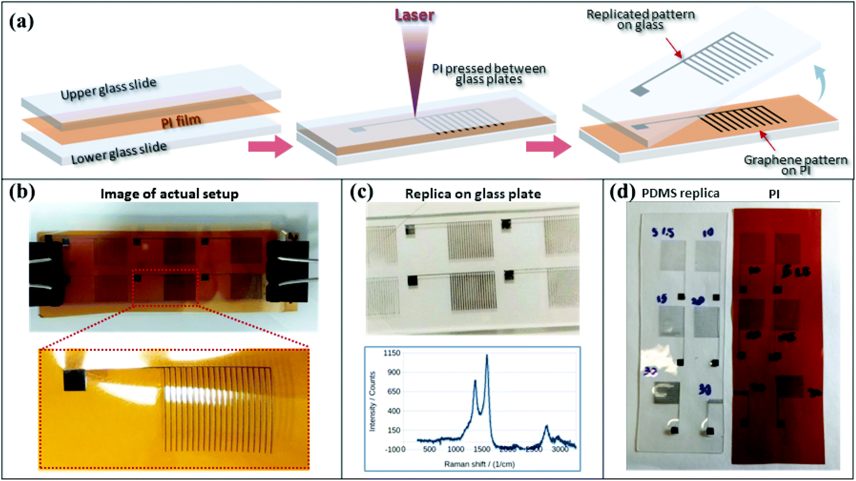 | ||
| Fig. 1 (a) Illustration of the local arrangement for simultaneous LIG and LIBT of graphene patterns; (b) photograph of the setup after writing interdigitated capacitor test patterns, with the paper clips used for keeping the layers of the “sandwich” in contact. The lower image shows an individual LIG electrode written with good resolution (lines ∼25 μm thick); (c) an example of LIG electrode patterns transferred to a glass slide, with the presence of graphene confirmed by the graph exhibiting the characteristic Raman peaks from graphene; and (d) LIG patterns written in PI and the corresponding replication in a PDMS sheet. | ||
The reasons for the high adhesion of LIG to the glass and PDMS substrates have not yet been positively determined, although there are indications of glass melting at the surface in contact with the PI. For the PDMS, the picture is further complicated by the fact that, under appropriate experimental conditions, a 355 nm UV laser is able to carbonize the material, even if its optical absorption is very low at this wavelength.12 The resulting carbon patterns in the PDMS are expected to accumulate contributions from both LIG transfer and PDMS carbonization. The electrical resistivity of the patterns transferred to glass varies in a wide range, depending on the processing conditions. Until now, the sample with the best properties (on glass) exhibited a resistivity of 68 μΩ m−1, with the corresponding twin patterns in the PI displaying a value of 32 μΩ m−1.
Alternative ways to decorate the laser-induced graphene patterns have already been tested with very positive results. Gold films were deposited (by sputtering) on selected regions of the PI sheets prior to laser processing of electrodes for biological sensors. Fig. 2a shows a picture of one sensor, as well as SEM images of the resulting microstructure. Uniformly distributed gold droplets (in the 5 μm–10 μm range) embedded in a matrix of graphene sheets can be noticed in the image. The inset picture, showing a higher magnification, indicates that the confined environment during polymer graphitization forced the graphene sheets to assume a new, more compact configuration, different from the normal (unrestrained) “rosebud-like” morphology of LIG. Alternatively, the top glass in the sandwich can be coated with thick or thin films for simultaneous synthesis, doping/decoration and transfer. As an example of the application of this method, niobium films were sputtered on the top glass slide for direct laser fabrication of flexible hybrid MSCs. Fig. 2b shows a set of MSCs ready for testing, and a TEM high resolution image showing the presence of Nb2O5 grains (∼3 nm) among the graphene sheets.
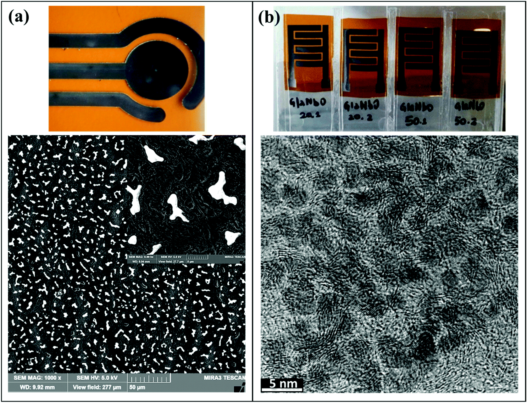 | ||
| Fig. 2 (a) Biological electrochemical sensor incorporating gold particles in the active circular region, with the corresponding SEM images showing gold droplets uniformly dispersed in the graphene matrix. The morphology of LIG in a confined environment seems to consist of more densely packed graphene sheets and (b) flexible graphene/Nb2O5 hybrid MSCs and the corresponding high resolution TEM image showing the nanometric scale oxide grains mixed with the graphene sheets. | ||
The electrochemical performances of the laser fabricated MSCs were evaluated using a two-electrode setup (in 1 M KOH), which is a commonly used electrolyte for practical applications in energy related devices. Fig. 3(a and b) show the results of cyclic voltammetry (CV) and galvanostatic charge/discharge (GCD) tests performed on PI-based MSCs, while Fig. 3(c and d) present the corresponding results for PI/Nb2O5 MSCs. The CV curves for PI/Nb2O5 MSCs have larger enclosed areas, as well as more symmetrical shapes when compared to the PI-based MSCs. Fig. 3e shows the areal capacitance versus scan rate curves for the laser-processed PI and the niobium-containing devices. Once again, the electrochemical charge storage performance of the MSCs was significantly improved by Nb2O5 incorporation. Fig. 3f shows the capacitance retention of a PI/Nb2O5 MSC device during repetitive CV cycles. The device exhibited outstanding cycling performance at a scan rate of 75 mV s−1. The capacitance retention decreased slightly up to 300 cycles, and after that it remained as high as ∼99% over 5000 cycles. The inset in Fig. 3f shows the shapes of typical CV curves without any significant deterioration, indicating a long cycle life.
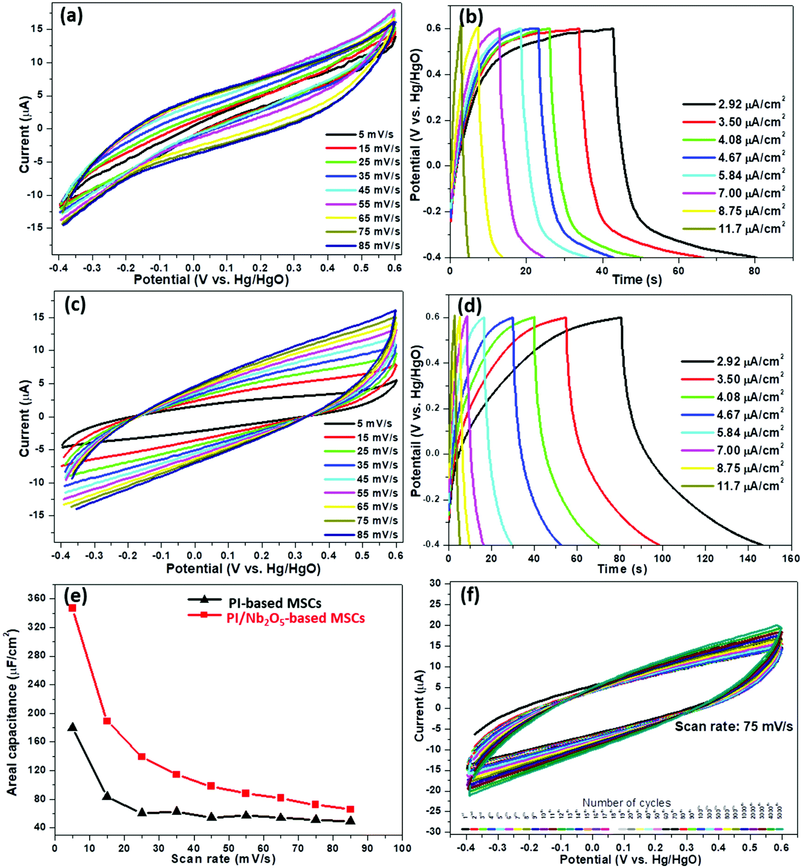 | ||
| Fig. 3 Electrochemical analysis of laser fabricated MSC devices. PI-based MSCs: (a) CV curves and (b) galvanostatic charge/discharge curves. PI/Nb2O5-based MSCs: (c) CV curves and (d) galvanostatic charge/discharge curves. Comparison of specific capacitances of PI and PI/Nb2O5-based MSCs: (e) specific capacitance vs. the scan rate. (f) Capacitance retention of niobium-containing MSCs for 5000 charge/discharge cycles. Inset: CV curves measured at regular intervals during the repetitive cycling test. | ||
Forward transfer of the graphene patterns to the underlying glass has also been successfully accomplished, using higher fluences and thinner PI sheets. The method is very straightforward, opening the possibility for simultaneous synthesis, doping/decoration and transfer of graphene patterns to arbitrary substrates at room temperature and pressure. The extreme local conditions during the confined induction of graphitization can probably help chemical reactions, doping and the intercalation of compounds in the multilayer graphene sheets.
Most researchers use CO2 laser cutters/engravers for photothermal LIG processing. This is probably the main reason for the technique to remain undiscovered until now, since the long infrared wavelengths cannot cross soda-lime-silica (or borosilicate) glass slides. In our experiments we used a frequency tripled NdYVO4 laser (Spectra Physics Pulseo 355-20), but the method could most probably be performed with other near UV, visible or near infrared lasers. The range of experimental conditions for successful LIG transfer to the glass and PDMS substrates was relatively wide (laser powers between 0.5 W and 9 W, pulse repetition rates 500 Hz–50 kHz, and laser spot sizes between 10 μm and 500 μm).
Conclusions
At this early stage in the research, there are still some outstanding practical problems that need to be solved (or, at least, circumvented). The more troublesome is the generation of liquid by-products during the carbonization process. Due to the confined environment, the liquid may gradually accumulate, interfering with the cooling rate of the treated material and the optical path of the laser (due to bubble formation). Depending on the processing conditions, the thickness of the PI layer and the design and dimensions of the laser-treated device, the writing/transfer processes might not be affected, with very good final results. On the other hand, under extremely unfavourable conditions, the written device may be riddled with defective regions due to the irregular attachment of the graphene flakes upon separation of the sandwich.The methodology for laser processing reported in this communication ultimately allows the growth/deposition of graphene patterns on a wide variety of substrates. Besides being simple, convenient and inexpensive, the approach is very flexible, providing several ways to simultaneously perform multiple modifications to the material. By using an experimental arrangement which can be described as “contact LIFT” (or “contact LIBT”, for backward transfer of the synthesized graphene), other parameters related to the confined nature of the synthesis environment are open to study and exploitation.
Conflicts of interest
The authors declare no conflict of interest.Acknowledgements
This research work was financially supported by the Science and Engineering Research Board (SERB), Department of Science & Technology (DST), New Delhi, India (SB/S2/RJN-159/2017) and the Japan Society for the Promotion of Science (JSPS), Japan (JSPS KAKENHI Grant No.18F18063).References
- A. K. Geim and K. S. Novoselov, Nat. Mater., 2007, 6, 183–191 CrossRef CAS PubMed
.
- K. S. Novoselov, V. I. Fal'ko, L. Colombo, P. R. Gellert, M. G. Schwab and K. Kim, Nature, 2012, 490, 192–200 CrossRef CAS PubMed
- M. Chen, R. C. Haddon, R. Yan and E. Bekyarova, Mater. Horiz., 2017, 4, 1054–1063 RSC
- H. C. Lee, W.-W. Liu, S.-P. Chai, A. R. Mohamed, A. Aziz, C.-S. Khe, N. M. S. Hidayah and U. Hashim, RSC Adv., 2017, 7, 15644–15693 RSC
- Y. Gao, J. Chen, G. Chen, C. Fan and X. Liu, Small Methods, 2021, 5, 2100771 CrossRef CAS PubMed
- R. Kumar, A. Pérez del Pino, S. Sahoo, R. K. Singh, W. K. Tan, A. Matsuda and E. Joanni, Prog. Energy Combust. Sci., 2022, 91, 100981 CrossRef
- R. Kumar, R. K. Singh, D. P. Singh, E. Joanni, R. M. Yadav and S. A. Moshkalev, Coord. Chem. Rev., 2017, 342, 34–79 CrossRef CAS
- J. Lin, Z. Peng, Y. Liu, F. Ruiz-Zepeda, R. Ye, E. L. G. Samuel, M. J. Yacaman, B. I. Yakobson and J. M. Tour, Nat. Commun., 2014, 5, 5714 CrossRef CAS PubMed
- R. Ye, D. K. James and J. M. Tour, Acc. Chem. Res., 2018, 51, 1609–1620 CrossRef CAS PubMed
- R. Ye, D. K. James and J. M. Tour, Adv. Mater., 2019, 31, 1803621 CrossRef PubMed
- E. C. P. Smits, A. Walter, D. M. d. Leeuw and K. Asadi, Appl. Phys. Lett., 2017, 111, 173101 CrossRef
- Y. Zhu, H. Cai, H. Ding, N. Pan and X. Wang, ACS Appl. Mater. Interfaces, 2019, 11, 6195–6200 CrossRef CAS PubMed
| This journal is © The Royal Society of Chemistry 2022 |