DOI:
10.1039/D2NR01635D
(Paper)
Nanoscale, 2022,
14, 7561-7568
Phase transition and nanomechanical properties of refractory high-entropy alloy thin films: effects of co-sputtering Mo and W on a TiZrHfNbTa system†
Received
25th March 2022
, Accepted 6th April 2022
First published on 7th April 2022
Abstract
Refractory high-entropy alloys (RHEAs) that consist of multiple principal refractory elements have attracted significant attention due to their many interesting and useful properties for structural applications. However, so far, a vast majority of reports on RHEAs focused on a few well-known compositions such as NbMoTaW, NbMoTaWV, and TiZrHfNbTa. The discovery of new RHEAs with enhanced mechanical properties has been highly desirable. Here we produce two new RHEA thin films – TiZrHfNbTaMo and TiZrHfNbTaW, by co-sputtering Mo or W on a previously studied TiZrHfNbTa RHEA system. The TiZrHfNbTaMo and TiZrHfNbTaW thin films exhibit an amorphous state, while the TiZrHfNbTa one shows a nanocrystalline structure. Using the nanoindentation method, we show that the addition of Mo or W in the TiZrHfNbTa during the co-sputtering process increases the hardness while resulting in comparable elastic moduli. Through the strain rate sensitivity tests of the thin films, we obtain their activation volumes and discuss their deformation mechanisms in the nanoindentation tests.
 Yu Zou | Yu Zou is an assistant professor and Dean's Spark Professor in the Department of Materials Science & Engineering at the University of Toronto (U of T). He received his doctorate, master's, and bachelor's degrees from ETH Zurich, McGill University, and Beihang University, respectively, all in Materials Science and Engineering. He was also a JSPS visiting scholar at Kyoto University. He did his postdoctoral research in the Department of Mechanical Engineering at Massachusetts Institute of Technology before he joined the faculty at U of T in 2018. At U of T, he leads the Laboratory for Extreme Mechanics and Additive Manufacturing (LEMAM), and his research interests include nanocrystalline alloys, nanomechanical testing, metal additive manufacturing, and machine learning for alloy design and advanced manufacturing. He has received the Minerals, Metals and Materials Society (TMS) 2022 Early Career Faculty Fellow Award, 2021 Young Leaders Professional Development Award, 2022 Ontario Early Researcher Award, and 2020 Journal of Materials Research (JMR) Early Career Scholars Prize. He is currently serving as the Chair of the Materials Technical Section in the Metallurgy and Materials Society of CIM (MetSoc) in Canada. |
Introduction
Since the concept of high-entropy alloys (HEAs) was introduced about 18 years ago, many interesting structures and properties have been discovered for critical engineering applications.1–7 Refractory high-entropy alloys (RHEAs) are typically composed of four or more multiple principal elements from IV, V, and VI groups;8–11 many RHEAs show excellent thermal stability and mechanical properties such as high strength and hardness at elevated temperatures.12–17 Compared with bulk-state and coarse-grain RHEAs,9 a few nanocrystalline RHEAs exhibit a promising combination of high strength, stability, and ductility.11,18 Modifying the RHEA composition provides an opportunity to obtain further enhanced mechanical properties for structural applications. For example, the well-studied body-centered cubic (bcc) NbMoTaW and NbMoTaWV systems suffer from low-temperature brittleness, but bcc TiZrHfNbTa shows excellent ductility at room temperature.19,20 Moreover, based on the direct current (DC) magnetron co-sputtering technique, our previous studies have successfully fabricated nanocrystalline TiZrHfNbTa thin films and determined the relationship between the composition ratio (TiZrHf to NbTa) and mechanical properties.21 However, despite their enhanced mechanical performance at room temperature, the strength of the TiZrHfNbTa system decreases rapidly with increasing temperature, hindering its high-temperature applications.20 Therefore, it is critical to discover new and useful RHEA systems in a larger compositional space.
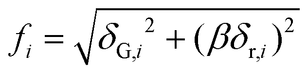
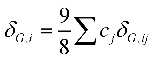
Solid solution strengthening (SSS) is one of the major strengthening mechanisms in HEAs: the strength increment is attributed to the mismatch of both shear moduli δG,i and atomic radii δr,i of various solute elements, which can be estimated by:17,19
where the average shear modulus of HEAs
Gmix is calculated based on the rule of mixtures,
20 the material-dependent dimensionless parameter
A equals 0.04,
19 and the interaction force parameter of element
i fi is related to the shear modulus
G and atomic size
r:
17| |  | (2) |
where
β depends on the type of the mobile dislocation, generally ranging 2–4 for screw dislocations and higher than 16 for edge dislocations.
19 For the single-phase bcc HEAs, the corresponding mismatches of shear modulus
δG,i and atomic size
δr,i can be determined by the following equations, respectively:
19,22| |  | (3) |
| |  | (4) |
where
δG,i = 2(
Gi –
Gj)/((
Gi +
Gj)) and
δr,i = 2(
ri –
rj)/((
ri +
rj)). Accordingly, the corresponding Δ
σss for the NbMoTaW is about 1620 MPa (ref.
23) while that for TiZrHfNbTa is about 938 MPa.
20 The lower strength in TiZrHfNbTa could be attributed to the lower shear moduli of all their components. Introducing an element with a higher shear modulus into the TiZrHfNbTa could provide a new opportunity to increase the strength. For example, by adding Mo (
G = 125 GPa (ref.
24)), the corresponding TiZrHfNbTaMo system
20 exhibits a significant SSS effect (Δ
σss = 1669 MPa) at room temperature and enhanced strengths in a wide temperature range,
i.e., improved plasticity at room temperature and strength at high temperatures. Similarly, adding W (
G = 160 GPa (ref.
24)) to the TiZrHfNbTa system also shows a potential to enhance Δ
σss (about 1750 MPa based on
eqn (1)–(4)). Hence, both TiZrHfNbTaMo and TiZrHfNbTaW systems are promising RHEA candidates with improved mechanical properties. However, so far, both RHEAs have been rarely studied, particularly for nanocrystalline RHEAs.
In this work, we fabricate TiZrHfNbTa, TiZrHfNbTaMo, and TiZrHfNbTaW RHEA thin films using DC magnetron co-sputtering and study their mechanical properties through the nanoindentation method. We also employ strain rate sensitivity tests to evaluate the strain-rate sensitivity and determine the corresponding activation volumes of the three RHEAs. Our study offers a new opportunity to modify the structure and improve the mechanical properties of RHEAs.
Experimental
By the DC magnetron co-sputtering method, we deposited TiZrHfNbTa, TiZrHfNbTaMo, and TiZrHfNbTaW HEA thin films on (100) silicon substrates at room temperature using equiatomic TiZrHf and NbTa targets, as well as Mo and W targets (99.9%, targets from MaTeck GmbH), as shown in Fig. S1.† The chamber base pressure was kept below 10−6 mbar, and the target–substrate distance and the power of the magnetron were adjusted to ensure equal arriving ratios of all the elements. The substrate was fixed with rotation (30 rpm) to obtain a homogeneous composition distribution of each element. Simultaneously, the ion beam-assisted deposition (IBAD) technique was applied to decrease the grain size using a broad ion beam source (KRI KDC 40, a beam energy of 1.2 keV, a current of 5 mA, and an incidence angle of 35°). The morphologies and composition of the films were characterized using a Hitachi SU5000 and SU7000 FESEM; the structure was identified by X-ray diffraction (Bruker D8 Discover, Cu-Kα1).
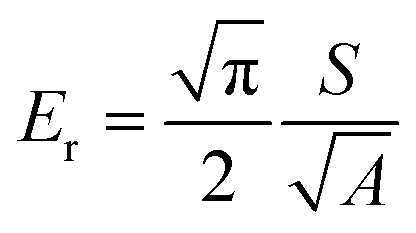
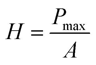
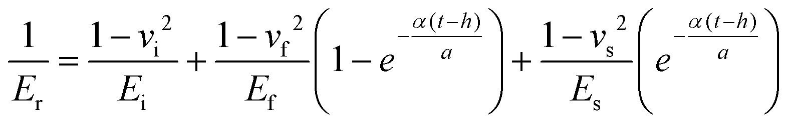
The nanoindentation tests were carried out using a KLA iMicro nanoindenter with a diamond Berkovich tip (Synton-MDP, Switzerland). During the measurement, the tip penetrates the sample to a depth h, and the reduced elastic modulus Er and nanohardness H were calculated using equations:25,26
| |  | (5) |
| |  | (6) |
where
S is the stiffness of the contact,
i.e., the slope of the unloading curve,
A the projected area of the indenter at the contact depth
h, equal to 24.5
h2 for a Berkovich tip, and
Pmax the load at the maximum point of the load–displacement curve. The hardness and elastic modulus at various depths and strain rates were measured using the advanced dynamic
E and
H and constant displacement rate indentation methods, both of which apply a continuous stiffness measurement with an oscillation frequency of 110 Hz and a data acquisition rate of 500 Hz. The corresponding displacement rates in strain rate sensitivity tests were 5, 10, 20, and 40 nm s
−1. The elastic modulus of the test specimen
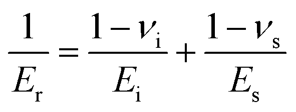
Es can then be calculated based on the following relationship from contact mechanics:
| |  | (7) |
where
ν is Poisson's ratio and the subscript i indicates a property of the indenter material (
Ei = 1140 GPa and
νi = 0.07 for a diamond tip). To eliminate the substrate effect, the modified King's model for Berkovich indenter
27 can be applied to calculate the elastic modulus of the film (
Ef):
| |  | (8) |
where
Es and
vs are the elastic modulus (169 GPa) and Poisson's ratio (0.28) of the silicon substrate,
28a is the square root of the projected contact area,
t is the thickness of the film,
h is the displacement, and
α is a numerically determined scaling parameter depending on the function of
a/
t27 (the corresponding values of different films are listed in
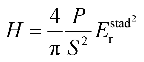
Table 1). The corresponding nanohardness can be determined as:
21| |  | (9) |
where
P/
S2 is the load/stiffness
2 value and
Estadr is the calculated standard reduced modulus ignoring the substrate effect,
i.e.,
a/
t → 0.
Table 1 The measured thickness of TiZrHfNbTa, TiZrHfNbTaMo, and TiZrHfNbTaW, and the corresponding calculated scaling parameter α
| Sample |
Thickness (nm) |
α
|
| TiZrHfNbTa |
585 |
1.866 |
| TiZrHfNbTaMo |
688 |
1.755 |
| TiZrHfNbTaW |
655 |
1.788 |
The atomic-scale nanostructures were constructed using Atomsk29 based on the measured grain size (Table 1). The corresponding schematics of the element, grain or cluster, and strain distributions were obtained using OVITO.30
Results and discussion
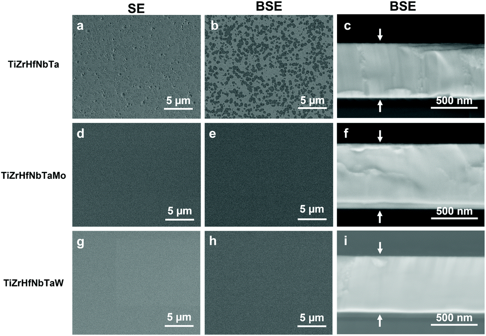
Fig. 1 shows the surface and cross-sectional morphologies of the as-deposited TiZrHfNbTa, TiZrHfNbTaMo, and TiZrHfNbTaW thin films. The dense cross-sections demonstrate the successful fabrication of nanoscale thin films. Compared with the samples with Mo or W additions, TiZrHfNbTa exhibits a relatively rough surface with small dimples distributed uniformly. This morphology could be attributed to the oxidation of TiZrHfNbTa.21Table 1 lists the measured thickness of TiZrHfNbTa, TiZrHfNbTaMo, and TiZrHfNbTaW, which are 585, 688, and 655 nm, respectively.
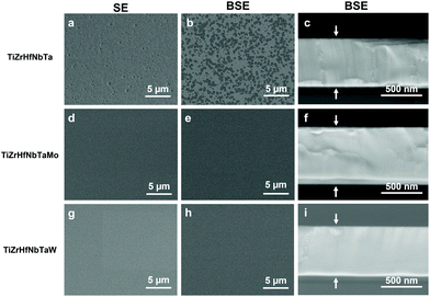 |
| | Fig. 1 Secondary electron (SE) and backscattered electron (BSE) images of the top view and cross-section of the as-deposited (a–c) TiZrHfNbTa, (d–f) TiZrHfNbTaMo, and (g–i) TiZrHfNbTaW thin films. | |
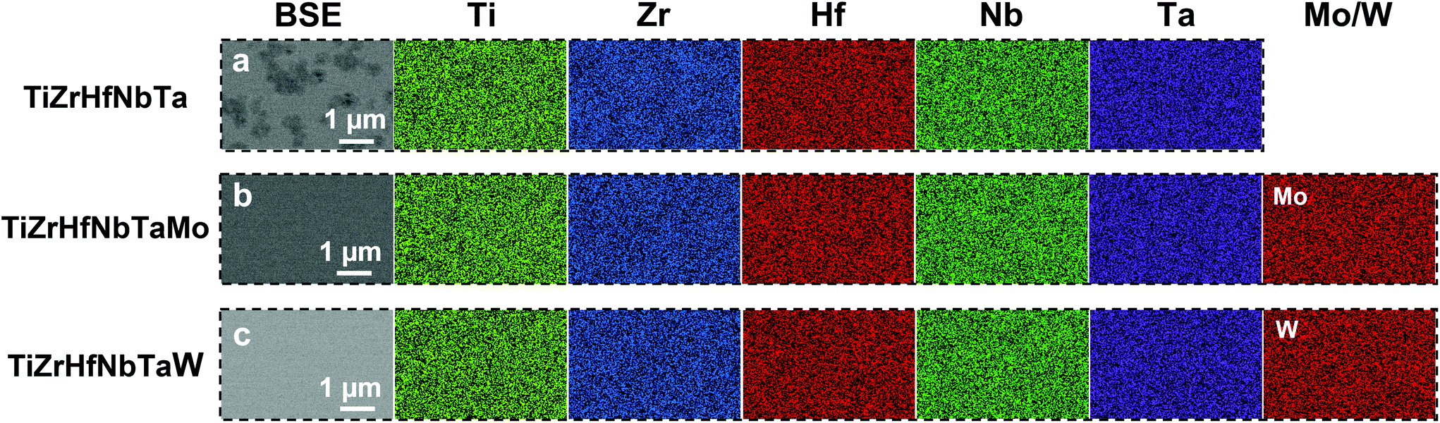
As shown in the EDS results (Fig. 2), all the elements are homogeneously distributed without obvious segregation. The oxygen concentration in TiZrHfNbTa is higher than those of TiZrHfNbTaMo and TiZrHfNbTaW (Table 2), which is probably due to the smallest thickness of TiZrHfNbTa film. Fig. S2† presents the element distribution of the sample cross-sections. The oxide layers on the surface are thin (<100 nm), and the oxygen (O) signal can barely be detected by the EDS detector. In contrast, there is an obvious oxide layer between the HEA film and the silicon substrate, attributed to the silicon oxide on the raw silicon wafer. Hence, more O signals from silicon oxide can penetrate the thinnest HEA film (TiZrHfNbTa), leading to the highest O concentration in the top-view EDS characterization. Based on the cross-section mapping, all metallic elements are uniformly distributed along the depth direction, except Ta and W whose signals are overlapped by the strong signal of Si due to their close ionization energies.
 |
| | Fig. 2 EDS mapping results of (a) TiZrHfNbTa, (b) TiZrHfNbTaMo, and (c) TiZrHfNbTaW thin films. All three samples exhibit a uniform compositional distribution. | |
Table 2 The atomic ratios of all the elements and corresponding configuration entropy of TiZrHfNbTa, TiZrHfNbTaMo, and TiZrHfNbTaW samples. The oxygen concentration on TiZrHfNbTa is higher than on the samples with Mo or W additions
| Sample |
Atomic ratio (at%) |
Configurational entropy |
| Ti |
Zr |
Hf |
Nb |
Ta |
Mo |
W |
O |
| TiZrHfNbTa |
19.6 |
15.7 |
17.3 |
19.3 |
17.4 |
— |
— |
10.6 |
1.61R |
| TiZrHfNbTaMo |
17.0 |
14.1 |
15.3 |
16.6 |
15.3 |
16.9 |
— |
4.8 |
1.79R |
| TiZrHfNbTaW |
15.4 |
12.5 |
15.9 |
18.3 |
16.7 |
— |
17.1 |
4.0 |
1.78R |
Fig. 3 shows the XRD patterns of TiZrHfNbTa, TiZrHfNbTaMo, and TiZrHfNbTaW thin films. Compared with the TiZrHfNbTa that exhibits bcc structure, the samples with Mo or W addition show broadened (110) peaks. Fig. S3† presents the Bigaussian-fitted peaks of all the samples after normalization. Based on the peak position and width, the corresponding grain sizes are calculated using the Scherrer equation (Table 3). Although there is no discrete point, a grain size less than 3 nm can be regarded as a transition point from a nanocrystalline structure to an amorphous structure.31–33 Thus, the co-sputtered samples with Mo or W addition possess amorphous structures rather than a crystalline structure. According to previous research on magnetron co-sputtering,34–36 a highly mixing alloy tends to form a glass-like structure, i.e., the higher configurational entropy S the higher tendency to form an amorphous structure. This relationship between entropy (S) and amorphous structure also agrees with the glass-forming ability of HEAs37,38 and corresponds well to the results of nanocrystalline TiZrHfNbTa with a lower S and amorphous TiZrHfNbTaMo and TiZrHfNbTaW with larger S values (Table 2).
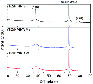 |
| | Fig. 3 The XRD patterns of the TiZrHfNbTa, TiZrHfNbTaMo, and TiZrHfNbTaW samples. All three samples exhibit bcc structure while the peaks of TiZrHfNbTaMo and TiZrHfNbTaW are significantly broadened, indicating amorphous structures. | |
Table 3 The (110) peak positions, corresponding lattice constants, full width at half maximum (FWHM), and the calculated grain sizes of the TiZrHfNbTa, TiZrHfNbTaMo, and TiZrHfNbTaW samples
| Sample |
2θ(110) (°) |
Lattice constant (Å) |
FWHM (°) |
Grain size (nm) |
|
| TiZrHfNbTa |
37.18 |
3.417 |
0.29 |
29.0 |
| |
| TiZrHfNbTaMo |
37.40 |
3.398 |
4.74 |
1.8 |
Amorphous |
| TiZrHfNbTaW |
37.46 |
3.393 |
4.86 |
1.7 |
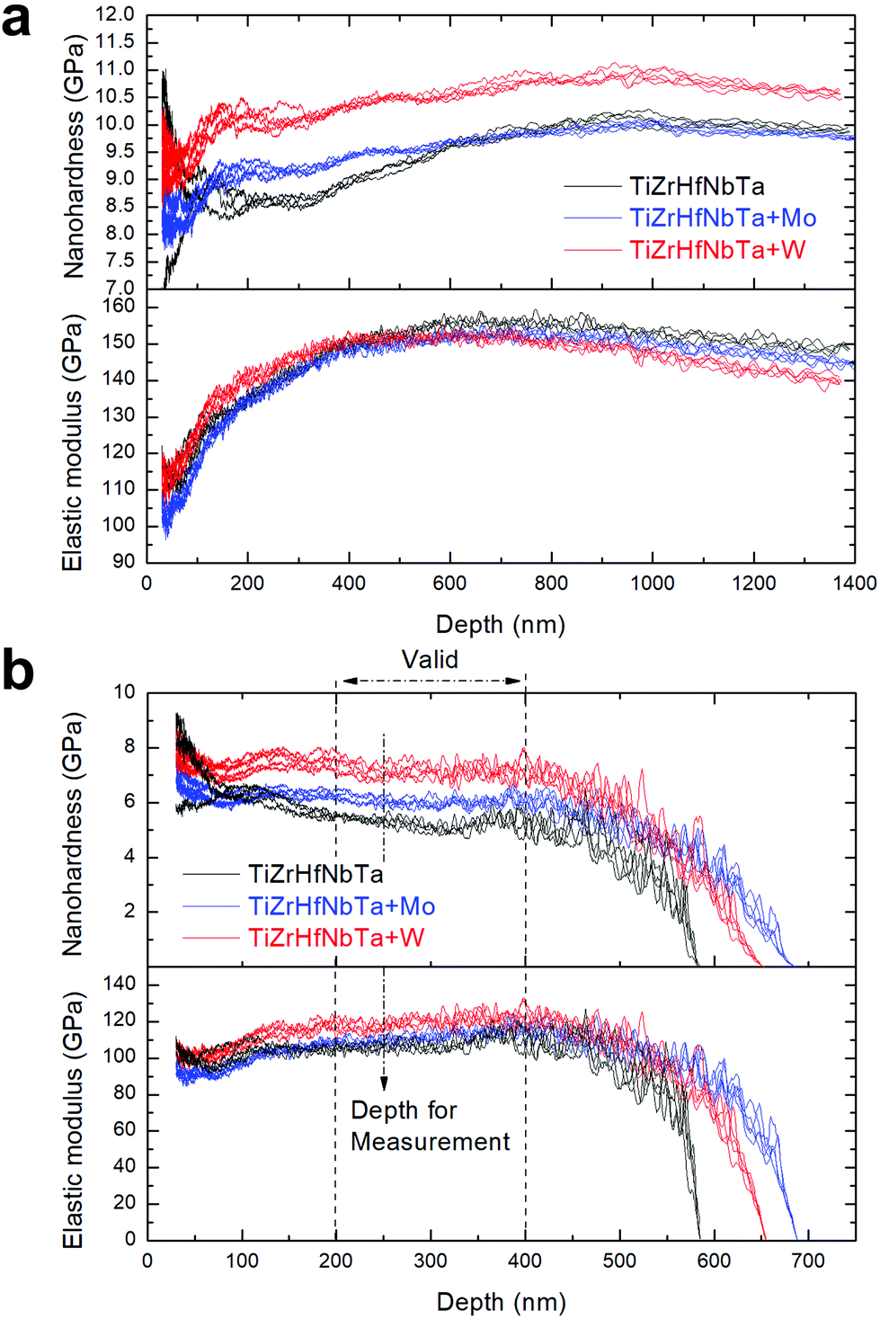
Fig. 4a shows the measured E and H at depths ranging from 10 to 1400 nm. The TiZrHfNbTaW exhibits the highest hardness, while the elastic moduli are similar for all. The obvious variation occurs at low depths (<200 nm), which could be attributed to the roughness of the thin film and changes in the indenter geometry;39 the most significant variation appears below 100 nm, corresponding well to the thin oxide layer on the sample surface (Fig. S2†). Meanwhile, TiZrHfNbTa exhibits a larger variance of hardness in the low depth range than TiZrHfNbTaMo and TiZrHfNbTaW, corresponding to a rougher surface with small dimples (Fig. 1a and b). In response, reliable data should be obtained at a larger depth. Since the film is thin in thickness (<700 nm), the measured E and H at high depths (>400 nm) were significantly affected by the silicon substrate. Fig. 4b presents the calculated values eliminating the substrate effect based on the modified King's model,27 whose valid region is about 70% of the total thickness. Accordingly, the data measured at 200–400 nm are more stable and reliable, and therefore the E and H at a depth of 250 nm are used to minimize both the effects from surface and substrate for evaluating the mechanical properties of all the samples.
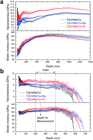 |
| | Fig. 4 (a) Nanohardness and elastic modulus as functions of the depth in the as-deposited HEA thin films. (b) The corrected nanohardness and elastic modulus based on the modified King's model.27 A depth of 250 nm is selected for further measurement. | |
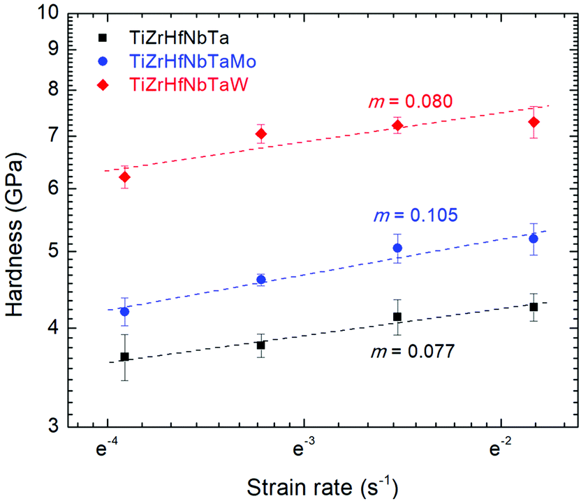
To elucidate the dominant deformation mechanisms of the HEA samples, nanoindentation was performed at different displacement rates ḣ. From the results, it was observed that the tested hardness H increases as ḣ increases. The corresponding strain rate sensitivity (SRS) m can be determined using the equation:
| |  | (10) |
where the strain rate

can be calculated based on

(the depth
h is 250 nm).
Fig. 5 plots
H versus
on a logarithmic scale, where the slopes of the lines are the corresponding values of
m. The activation volume
Va, which is a mechanistic indicator during plastic deformation, can be determined by the following equation:
40| |  | (11) |
where
k is the Boltzmann constant,
T is the test temperature, and
C is a deformation-dependent constant and is 3.
41,42 At a relatively low strain rate (0.02 s
−1,
i.e., 5 nm s
−1), both TiZrHfNbTaMo and TiZrHfNbTaW exhibit a much smaller variance than TiZrHfNbTa, indicating that the systems with Mo or W additions may be inclined to a more consistent deformation mechanism over a wider range of strain rates.
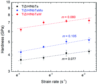 |
| | Fig. 5 The hardness as a function of the strain rate on a logarithmic scale. The slope corresponds to the strain rate sensitivity of TiZrHfNbTa, TiZrHfNbTaMo, and TiZrHfNbTaW. | |
On the one hand, based on previous nanoindentation studies of HEAs with similar compositions (Table 4),41–44 the calculated Va values of TiZrHfNbTa (2.1 b3) identify the deformation mechanism as dislocation nucleation in a few atomic volumes. On the other hand, a few other studies indicate that these low activation volumes are attributed to the cooperative migration of several atoms41,42,44,45 or thermally activated diffusion processes at grain boundaries.46,47 However, due to the slow self-diffusion rates of refractory elements at the room temperature48 and lower diffusivity in equiatomic HEAs than in pure metals,49 atom migration is unlikely to occur even in a pressure gradient under the nanoindenter tip. Different from dislocation mechanisms in the nanocrystalline TiZrHfNbTa, shear transformation zones (STZ) related mechanisms are considered the deformation mechanism in the amorphous TiZrHfNbTaMo and TiZrHfNbTaW.50 Diffusion processes may govern the plastic deformation of the amorphous TiZrHfNbTaMo and TiZrHfNbTaW,51 leading to more consistent SRS in a wide range of strain rates.
Table 4 The measured activation volumes Va and corresponding deformation mechanisms in this work and references. b is the Burgers vector of a/2 [111]
| HEA |
Method |
V
a (b3 or Å3) |
Possible mechanisms |
| TiZrNbTa43,44 |
Nanoindentation |
1–3 b3 |
Dislocation nucleation or migration of multiple atoms |
| TiZrNbTaMo43,44 |
| |
| TiZrHfNb41,42 |
Nanoindentation |
3–5 b3 |
|
| |
| TiZrHfNbTa52,53 |
Stress relaxation |
20–80 b3 |
Peierls–Nabarro52 or Kink-pair42 |
| |
| TiZrHfNbTa |
Nanoindentation |
2.1 b3 (52.2 Å3) |
Dislocation nucleation |
| TiZrHfNbTaMo |
33.6 Å3 |
Diffusion-related mechanism51 |
| TiZrHfNbTaW |
38.6 Å3 |
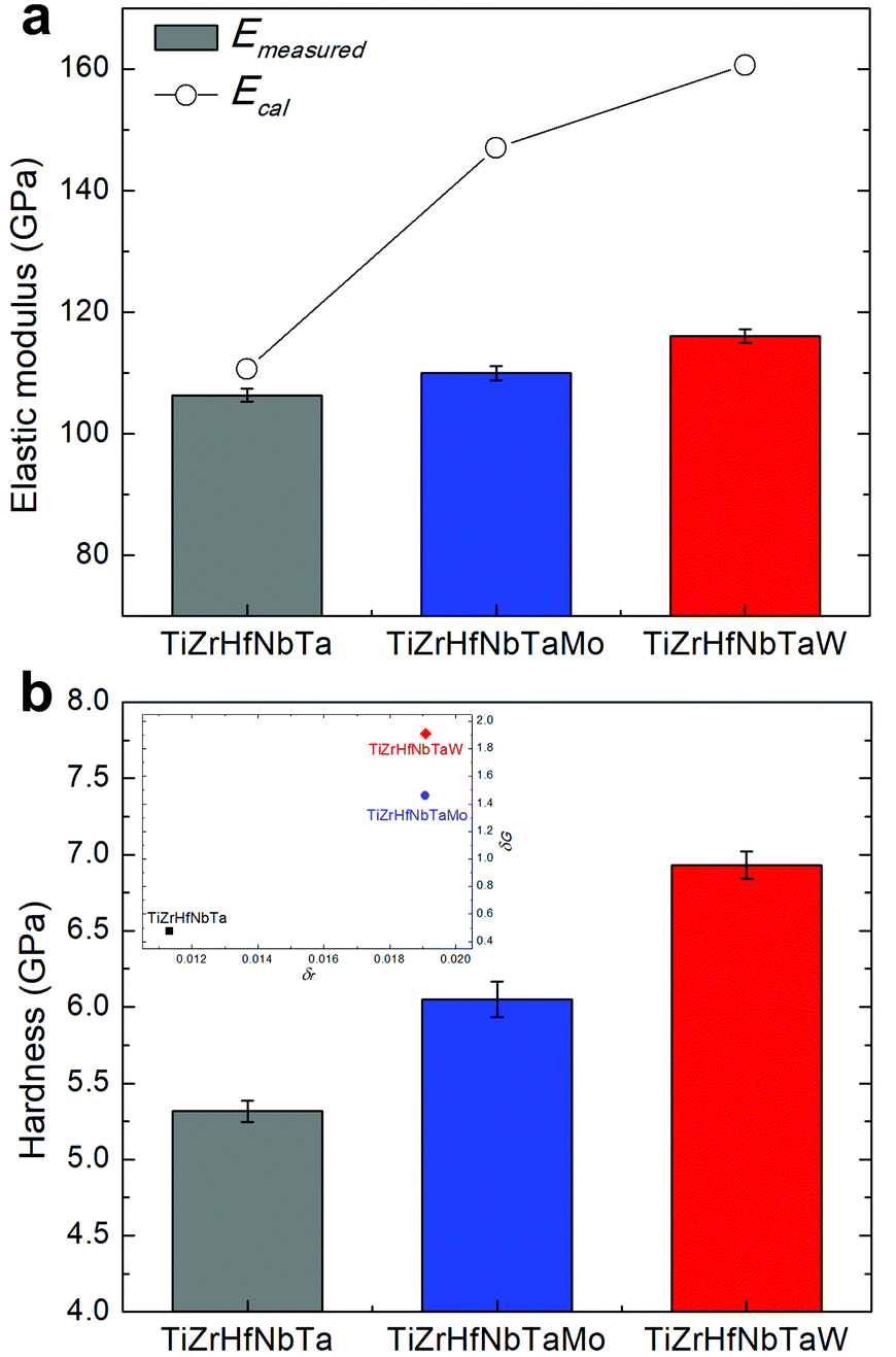
In contrast to the calculated values based on the rule of mixtures ( ), the values of indentation-measured elastic moduli Emeasured are comparable for the three compositions with only slight increment after Mo or W addition (Fig. 6a). Due to the absence of ordering of internal atomic shifts,54 the increasing volume fraction of triple junction,31,32 and substantial interface with excess free volume,55 the elastic modulus of amorphous materials is generally lower than that of the nanocrystalline state.56,57 Thus, the amorphous state in TiZrHfNbTaMo and TiZrHfNbTaW leads to lower elastic moduli, compensating the increment from Mo or W addition and resulting in similar modulus values of all the compositions.
 |
| | Fig. 6 The nanoindentation measured (a) elastic moduli and (b) hardness of TiZrHfNbTa, TiZrHfNbTaMo, and TiZrHfNbTaW. The open circles in (a) indicate the calculated values based on the rule of mixtures. The inserted figure in (b) presents the calculated mismatches of shear modulus δG and atomic size δr. | |
The measured hardness Hmeasured of the TiZrHfNbTaMo and TiZrHfNbTaW is higher than that of the TiZrHfNbTa (Fig. 6b). Based on the conventional SSS mechanism, both δG and δr in the samples with Mo or W addition are larger than those of the TiZrHfNbTa, implying a higher strengthening effect and leading to larger hardness values. However, it should be noted that the SSS effect in the amorphous structure is different from the bcc solid solution phase.58,59 On the one hand, there is no dislocation in the amorphous structure, and thus, the plastic deformation through shear banding is more difficult than that based on dislocation mechanisms. On the other hand, the strengthening mechanism might also be regarded as a mixed solution of nanocrystallite precipitations distributed in the amorphous matrix.60–62Fig. 7a and b illustrate the schematics of nanocrystalline and amorphous structures, respectively. Unlike the nanocrystalline one, randomly scattered precipitates may exist in the amorphous structure (Fig. S4†). After introducing a ½ 〈111〉 screw dislocation, which is typically governing the plastic deformation mechanism in TiZrHfNbTa,52 or a comparable defect in the amorphous one, nanocrystalline and amorphous materials exhibit distinct strain fields (Fig. 7c–f and Fig. S5†) relatively uniform and obviously scattered, respectively. Small nanocrystallites may act as strengthening media in the amorphous structures. Due to the significant differences between Mo/W from other elements, especially in elastic modulus, it could be assumed that the Mo- or W-rich nanocrystallites can provide improved local stress during the plastic deformation, serving as the reinforcement in the amorphous HEA matrix and leading to the enhanced hardness. The hardness difference between TiZrHfNbTaMo and TiZrHfNbTaW is probably attributed to the different elastic moduli of Mo (329 GPa) and W (411 GPa). A nanocrystallite composed of components with a higher modulus could lead to a stronger strengthening effect in the amorphous matrix.
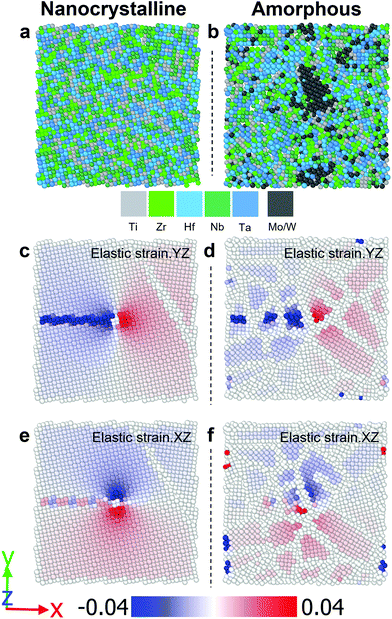 |
| | Fig. 7 The schematics of (a) nanocrystalline and (b) amorphous materials after introducing a ½ 〈111〉 screw dislocation at the center and the corresponding elastic strain fields at (c and d) YZ and (e and f) XZ planes. | |
Conclusions
In this study, we have fabricated TiZrHfNbTa, TiZrHfNbTaMo, and TiZrHfNbTaW RHEA thin films using the DC magnetron co-sputtering technique, identified their structures, and tested their elastic moduli and hardness using the nanoindentation method. The following results have been obtained:
1. TiZrHfNbTaMo and TiZrHfNbTaW thin films exhibit amorphous structures, while TiZrHfNbTa shows a nanocrystalline structure. Adding Mo or W element to the TiZrHfNbTa system leads to the crystalline-to-amorphous transition in the DC magnetron co-sputtered RHEAs. All the elements are uniformly distributed on the three RHEAs, forming solid solutions.
2. TiZrHfNbTa, TiZrHfNbTaMo, and TiZrHfNbTaW shows average elastic moduli of 106.3, 110.0, and 116.1 GPa, respectively, and average nanohardness of 5.32, 6.05, and 6.93 GPa, respectively. Mo- and W-rich nanocrystallites in the amorphous HEA matrix lead to the improved strength of TiZrHfNbTaMo and TiZrHfNbTaW; however, the amorphous states compensate for the elastic modulus increment from Mo and W additions, leading to comparable elastic modulus values to that of the nanocrystalline TiZrHfNbTa.
3. Through the nanoindentation SRS testing, we have obtained the average SRS values of TiZrHfNbTa, TiZrHfNbTaMo, and TiZrHfNbTaW are 0.077, 0.105, and 0.080, prospectively, and their average activation volumes are 2.1 b3 (52.2 Å3), 33.6 Å3, and 38.6 Å3, respectively.
4. Both Mo and W additions can facilitate the formation of the amorphous structure, leading to enhanced hardness and reduced elastic modulus.
Author contributions
Changjun Cheng: investigation, formal analysis, visualization, data curation, writing – original draft. Xiaofu Zhang: resources. Michel Haché: investigation. Yu Zou: Supervision, writing – review and editing.
Conflicts of interest
There are no conflicts to declare.
Acknowledgements
The authors thank Dr Yanan Liu (Department of Earth Sciences, University of Toronto) and Sal Boccia (Department of Materials Science and Engineering, University of Toronto) for the experimental support. C. C., M. H., and Y. Z. acknowledge the financial support from the Discovery Grants Program (Grant No. RGPIN-2018-05731) of the Natural Sciences and Engineering Research Council of Canada (NSERC), New Frontiers in Research Fund – Exploration (NFRFE-2019-00603), and Dean's Spark Assistant Professorship in the Faculty of Applied Science & Engineering at the University of Toronto. M. J. R. H. acknowledges the financial support from Vanier Canada Graduate Scholarship (NSERC), Ontario Graduate Scholarship, Queen Elizabeth II/Eleanor and Burnett Thall Graduate Scholarship, and the Canada Foundation for Innovation (CFI)-John R. Evans Leaders Fund (JELF) Project# 38044.
References
- J.-W. Yeh, S.-K. Chen, S.-J. Lin, J.-Y. Gan, T.-S. Chin, T.-T. Shun, C.-H. Tsau and S.-Y. Chang, Adv. Eng. Mater., 2004, 6, 299–303 CrossRef CAS.
- B. Cantor, I. T. H. Chang, P. Knight and A. J. B. Vincent, Mater. Sci. Eng., A, 2004, 375–377, 213–218 CrossRef.
- Y. Zhang, T. T. Zuo, Z. Tang, M. C. Gao, K. A. Dahmen, P. K. Liaw and Z. P. Lu, Prog. Mater. Sci., 2014, 61, 1–93 CrossRef CAS.
- Y. F. Ye, Q. Wang, J. Lu, C. T. Liu and Y. Yang, Mater. Today, 2016, 19, 349–362 CrossRef CAS.
- D. B. Miracle and O. N. Senkov, Acta Mater., 2017, 122, 448–511 CrossRef CAS.
- M. C. Gao, D. B. Miracle, D. Maurice, X. Yan, Y. Zhang and J. A. Hawk, J. Mater. Res., 2018, 33, 3138–3155 CrossRef CAS.
- M. J. R. Haché, C. Cheng and Y. Zou, J. Mater. Res., 2020, 35, 1051–1075 CrossRef.
- O. N. Senkov, G. B. Wilks, D. B. Miracle, C. P. Chuang and P. K. Liaw, Intermetallics, 2010, 18, 1758–1765 CrossRef CAS.
- O. N. Senkov, G. B. Wilks, J. M. Scott and D. B. Miracle, Intermetallics, 2011, 19, 698–706 CrossRef CAS.
- S. Sheikh, S. Shafeie, Q. Hu, J. Ahlström, C. Persson, J. Veselý, J. Zýka, U. Klement and S. Guo, J. Appl. Phys., 2016, 120, 164902 CrossRef.
- X. Feng, J. Zhang, Z. Xia, W. Fu, K. Wu, G. Liu and J. Sun, Mater. Lett., 2018, 210, 84–87 CrossRef CAS.
- O. N. Senkov, D. B. Miracle, K. J. Chaput and J.-P. Couzinie, J. Mater. Res., 2018, 33, 3092–3128 CrossRef CAS.
- O. N. Senkov, J. M. Scott, S. V. Senkova, F. Meisenkothen, D. B. Miracle and C. F. Woodward, J. Mater. Sci., 2012, 47, 4062–4074 CrossRef CAS.
- M. C. Gao, C. S. Carney, Ö. N. Doğan, P. D. Jablonksi, J. A. Hawk and D. E. Alman, JOM, 2015, 67, 2653–2669 CrossRef CAS.
- C.-C. Juan, M.-H. Tsai, C.-W. Tsai, C.-M. Lin, W.-R. Wang, C.-C. Yang, S.-K. Chen, S.-J. Lin and J.-W. Yeh, Intermetallics, 2015, 62, 76–83 CrossRef CAS.
- O. N. Senkov, S. V. Senkova and C. Woodward, Acta Mater., 2014, 68, 214–228 CrossRef CAS.
- H. W. Yao, J. W. Qiao, J. A. Hawk, H. F. Zhou, M. W. Chen and M. C. Gao, J. Alloys Compd., 2017, 696, 1139–1150 CrossRef CAS.
- Y. Zou, J. M. Wheeler, H. Ma, P. Okle and R. Spolenak, Nano Lett., 2017, 17, 1569–1574 CrossRef CAS PubMed.
- O. N. Senkov, J. M. Scott, S. V. Senkova, D. B. Miracle and C. F. Woodward, J. Alloys Compd., 2011, 509, 6043–6048 CrossRef CAS.
- K.-K. Tseng, C.-C. Juan, S. Tso, H.-C. Chen, C.-W. Tsai and J.-W. Yeh, Entropy, 2019, 21, 15 CrossRef CAS PubMed.
- C. Cheng, X. Zhang, M. J. R. Haché and Y. Zou, Nano Res., 2021, 1–7 Search PubMed.
- L. A. Gypen and A. Deruyttere, J. Mater. Sci., 1977, 12, 1028–1033 CrossRef CAS.
- X.-G. Li, C. Chen, H. Zheng, Y. Zuo and S. P. Ong, npj Comput. Mater., 2020, 6, 70 CrossRef CAS.
- M. W. Guinan and D. J. Steinberg, J. Phys. Chem. Solids, 1974, 35, 1501–1512 CrossRef CAS.
- W. C. Oliver and G. M. Pharr, J. Mater. Res., 2004, 19, 3 CrossRef CAS.
- W. C. Oliver and G. M. Pharr, J. Mater. Res., 1992, 7, 1564–1583 CrossRef CAS.
- R. Saha and W. D. Nix, Acta Mater., 2002, 50, 23–38 CrossRef CAS.
- M. A. Hopcroft, W. D. Nix and T. W. Kenny, J. Microelectromech. Syst., 2010, 19, 229–238 CAS.
- P. Hirel, Comput. Phys. Commun., 2015, 197, 212–219 CrossRef CAS.
- A. Stukowski, Modell. Simul. Mater. Sci. Eng., 2009, 18, 015012 CrossRef.
- Y. Zhou, U. Erb and K. T. Aust, Philos. Mag., 2007, 87, 5749–5761 CrossRef CAS.
- Y. Zhou, U. Erb, K. T. Aust and G. Palumbo, Scr. Mater., 2003, 48, 825–830 CrossRef CAS.
- G. Palumbo, U. Erb and K. T. Aust, Scr. Metall. Mater., 1990, 24, 2347–2350 CrossRef CAS.
- D. Horwat, M. Dehmas, E. Aubry, J. Zollinger, S. Migot and J. F. Pierson, Intermetallics, 2009, 17, 421–426 CrossRef CAS.
- P. Y. Park, E. Akiyama, H. Habazaki, A. Kawashima, K. Asami and K. Hashimoto, Corros. Sci., 1995, 37, 307–320 CrossRef CAS.
- Z. Z. Tang, J. H. Hsieh, S. Y. Zhang, C. Li and Y. Q. Fu, Surf. Coat. Technol., 2005, 198, 110–113 CrossRef CAS.
- S. Guo, Q. Hu, C. Ng and C. T. Liu, Intermetallics, 2013, 41, 96–103 CrossRef CAS.
- S. Guo and C. T. Liu, Prog. Nat. Sci.: Mater. Int., 2011, 21, 433–446 CrossRef.
- Y.-F. Jia, Y.-Y. Cui, F.-Z. Xuan and F. Yang, RSC Adv., 2017, 7, 35655–35665 RSC.
- V. Maier-Kiener and K. Durst, JOM, 2017, 69, 2246–2255 CrossRef PubMed.
- Y. X. Ye, Z. P. Lu and T. G. Nieh, Scr. Mater., 2017, 130, 64–68 CrossRef CAS.
- Y. X. Ye, B. Ouyang, C. Z. Liu, G. J. Duscher and T. G. Nieh, Acta Mater., 2020, 199, 413–424 CrossRef CAS.
- S.-P. Wang, E. Ma and J. Xu, Intermetallics, 2018, 103, 78–87 CrossRef CAS.
- S.-P. Wang and J. Xu, J. Mater. Sci. Technol., 2019, 35, 812–816 CrossRef.
- D. Wu, J. S. C. Jang and T. G. Nieh, Intermetallics, 2016, 68, 118–127 CrossRef CAS.
- H. Höppel, J. May, P. Eisenlohr and M. Göken, Z. Metallkd., 2005, 96, 566–571 CrossRef.
- V. Maier, K. Durst, J. Mueller, B. Backes, H. W. Höppel and M. Göken, J. Mater. Res., 2011, 26, 1421–1430 CrossRef CAS.
- J. K. Mason, A. C. Lund and C. A. Schuh, Phys. Rev. B: Condens. Matter Mater. Phys., 2006, 73, 054102 CrossRef.
- S. Mridha, M. Sadeghilaridjani and S. Mukherjee, Metals, 2019, 9(2), 263 CrossRef CAS.
- I.-C. Choi, Y. Zhao, Y.-J. Kim, B.-G. Yoo, J.-Y. Suh, U. Ramamurty and J.-i. Jang, Acta Mater., 2012, 60, 6862–6868 CrossRef CAS.
- L. Krämer, V. Maier-Kiener, Y. Champion, B. Sarac and R. Pippan, Mater. Des., 2018, 155, 116–124 CrossRef.
- J. P. Couzinié, L. Lilensten, Y. Champion, G. Dirras, L. Perrière and I. Guillot, Mater. Sci. Eng., A, 2015, 645, 255–263 CrossRef.
- M. Feuerbacher, M. Heidelmann and C. Thomas, Philos. Mag., 2015, 95, 1221–1232 CrossRef CAS.
-
A. M. Glezer and N. Shurygina, Amorphous–Nanocrystalline Alloys, Taylor & Francis, CRC Press, Boca Raton, 2018 Search PubMed.
- Y. Zhou, S. Van Petegem, D. Segers, U. Erb, K. T. Aust and G. Palumbo, Mater. Sci. Eng., A, 2009, 512, 39–44 CrossRef.
- V. Kulikovsky, V. Vorlíček, P. Boháč, M. Stranyánek, R. Čtvrtlík, A. Kurdyumov and L. Jastrabik, Surf. Coat. Technol., 2008, 202, 1738–1745 CrossRef CAS.
- F. C. Li, T. Liu, J. Y. Zhang, S. Shuang, Q. Wang, A. D. Wang, J. G. Wang and Y. Yang, Mater. Today Adv., 2019, 4, 100027 CrossRef.
- D. S. Gianola, Z. Lee, C. Ophus, E. J. Luber, D. Mitlin, U. Dahmen, K. J. Hemker and V. R. Radmilović, Acta Mater., 2013, 61, 1432–1443 CrossRef CAS.
- D. Q. Ma, W. T. Jiao, Y. F. Zhang, B. A. Wang, J. Li, X. Y. Zhang, M. Z. Ma and R. P. Liu, J. Alloys Compd., 2015, 624, 9–16 CrossRef CAS.
- H. S. Kim, Scr. Mater., 2003, 48, 43–49 CrossRef CAS.
- J.-C. Lee, Y.-C. Kim, J.-P. Ahn, H.-S. Kim, S.-H. Lee and B.-J. Lee, Acta Mater., 2004, 52, 1525–1533 CrossRef CAS.
- F. B. Wu, S. K. Tien, W. Y. Chen and J. G. Duh, Surf. Coat. Technol., 2004, 177–178, 312–316 CrossRef CAS.
Footnote |
| † Electronic supplementary information (ESI) available: Schematic of magnetron co-sputtering, cross-sectional element distribution, normalized XRD peaks for grain size measurement, and schematics of deformation mechanisms of nanocrystalline and amorphous materials. See DOI: https://doi.org/10.1039/d2nr01635d |
|
| This journal is © The Royal Society of Chemistry 2022 |
Click here to see how this site uses Cookies. View our privacy policy here. 
 a,
Xiaofu
Zhang
a,
Xiaofu
Zhang


 can be calculated based on
  (the depth h is 250 nm). Fig. 5 plots H versus
 on a logarithmic scale, where the slopes of the lines are the corresponding values of m. The activation volume Va, which is a mechanistic indicator during plastic deformation, can be determined by the following equation:40
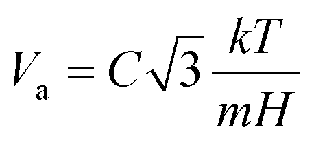
 ), the values of indentation-measured elastic moduli Emeasured are comparable for the three compositions with only slight increment after Mo or W addition (Fig. 6a). Due to the absence of ordering of internal atomic shifts,54 the increasing volume fraction of triple junction,31,32 and substantial interface with excess free volume,55 the elastic modulus of amorphous materials is generally lower than that of the nanocrystalline state.56,57 Thus, the amorphous state in TiZrHfNbTaMo and TiZrHfNbTaW leads to lower elastic moduli, compensating the increment from Mo or W addition and resulting in similar modulus values of all the compositions.