
Doped 2D SnS materials derived from liquid metal-solution for tunable optoelectronic devices†
Xiangyang
Guo‡
 a,
Yichao
Wang‡
ab,
Aaron
Elbourne
a,
Aishani
Mazumder
a,
Chung Kim
Nguyen
a,
Vaishnavi
Krishnamurthi
a,
Jerry
Yu
a,
Peter C.
Sherrell
c,
Torben
Daeneke
a,
Sumeet
Walia
a,
Yongxiang
Li
*a and
Ali
Zavabeti
*ac
a,
Yichao
Wang‡
ab,
Aaron
Elbourne
a,
Aishani
Mazumder
a,
Chung Kim
Nguyen
a,
Vaishnavi
Krishnamurthi
a,
Jerry
Yu
a,
Peter C.
Sherrell
c,
Torben
Daeneke
a,
Sumeet
Walia
a,
Yongxiang
Li
*a and
Ali
Zavabeti
*ac
aSchool of Engineering, RMIT University, Melbourne, VIC 3000, Australia. E-mail: yongxiang.li@rmit.edu.au
bSchool of Life and Environmental Sciences, Deakin University, Geelong, Victoria 3216, Australia
cDepartment of Chemical Engineering, The University of Melbourne, Parkville, Victoria 3010, Australia. E-mail: ali.zavabeti@unimelb.edu.au
First published on 21st April 2022
Abstract
Gas–liquid reaction phenomena on liquid-metal solvents can be used to form intriguing 2D materials with large lateral dimensions, where the free energies of formation determine the final product. A vast selection of elements can be incorporated into the liquid metal-based nanostructures, offering a versatile platform for fabricating novel optoelectronic devices. While conventional doping techniques of semiconductors present several challenges for 2D materials. Liquid metals provide a facile route for obtaining doped 2D semiconductors. In this work, we successfully demonstrate that the doping of 2D SnS can be realized in a glove box containing a diluted H2S gas. Low melting point elements such as Bi and In are alloyed with base liquid Sn in varying concentrations, resulting in the doping of 2D SnS layers incorporating Bi and In sulphides. Optoelectronic properties for photodetectors and piezoelectronics can be fine-tuned through the controlled introduction of selective migration doping. The structural modification of 2D SnS results in a 22.6% enhancement of the d11 piezoelectric coefficient. In addition, photodetector response times have increased by several orders of magnitude. Doping methods using liquid metals have significantly changed the photodiode and piezoelectric device performances, providing a powerful approach to tune optoelectronic device outputs.
1. Introduction
Inspired by the intriguing properties of two-dimensional (2D) materials, significant leaps in the synthesis and engineering of nanomaterials have been made.1,2 Several classes of 2D materials have been extensively studied; however, post-transition metal chalcogenides (PTMCs) have remained underexplored. Group IV mono-chalcogenide compounds, including SnS, SnSe, GeS, and GeSe, are typical PTMDs, showcasing promising semiconducting materials for high-performance optoelectronics,3,4 energy,5,6 thermoelectric,7 and nanogenerator technology.8 It has been previously reported that their bandgap offers optimal absorption in the solar spectrum and the piezoresponse is more than an order of magnitude in comparison to the conventionally used state-of-the-art materials.9 Despite the tremendous potential of PTMCs, exploiting PTMCs in practical device applications remain challenging due to the difficulty in synthesizing large area (100 μm) pinhole-free 2D layers. SnS, a representative PTMC group IV monochalcogenide has been widely employed in nanoelectronics, optoelectronics, visible-light photocatalysis, piezoelectric nanogenerator, mechanical, ferroelectric memory, and various other applications.10–12 Synthesis of 2D SnS has been established through the liquid metal route, and their applications in piezoelectricity and photodetection have been comprehensively studied.4,8 In particular, computational studies via density functional theory (DFT) have established newly formed boundary conditions for 2D SnS with a theoretical piezo-coefficient as between d11 ≈ 144 pm V−1 (relaxed-ion) and d11 ≈ 22 pm V−1 (clamped-ion).8,13 These results indicate a further potential to experimentally enhance the optoelectronic properties of 2D SnS to such potentially achievable values.13,14Several engineering routes to tune optoelectronics properties of 2D materials exist, including atomic substitutions, external charge transfer, insertion layer, electrostatic doping, Janus structure formations, defect engineering, zero-valent intercalation, floating gate modulation, and promoting the development of multi-functional devices.15–20 Doping of semiconductors is one the most established modification method for building tailored modern electronic components and devices.21,22 SnS doping has been reported using different techniques and metals such as Bi,23 Pb,24,25 Cu,26 In,27 Sb,28 Nd,29 Al,30 Fe,31 Ce,32 and Ag,33 which significantly altered their structure and composition to produce desirable optoelectronic properties. However, a controllable, facile and universal doping method has not been developed for 2D SnS.
In this work, liquid metal solutions are introduced as a reaction medium for the controlled synthesis of doped 2D SnS. Low melting point metals, including Bi and In, were mixed with Sn as a base liquid metal and exposed to H2S as a reactant gas. Uniquely, a self-limiting layer of doped 2D SnS was formed on the surface of liquid metal alloy. The 2D layers can be transferred to a desired substrate by touching the substrate to the droplet with ease. The transferred Bi2S3 and In2S3 doped 2D SnS feature uniform, pinhole-free nanosheets with hundreds of micrometers lateral dimensions. Adjusting the liquid metal alloy concentration ratios allowed for compositional doping to produce SnxInyS and SnxBiyS stoichiometries, with subsequently varied optoelectronic properties. SnxInyS with 6.4 at% SnxInyS has significantly enhanced the d11 piezo coefficient by ∼22.6% compared to previous studies, with the piezoelectric d11 coefficient reaching a value as high as ∼37.5 pm V−1.8 In contrast, the SnxBiyS sheets showed no observable piezoelectric effect. However, the SnxBiyS showed a remarkable improvement in photodetection at 0.1 at% Bi2S3 doping, where a substantial increase in fall times by several orders of magnitude was observed. Thus, this material can be used explicitly in neuromorphic applications such as artificial optoelectronic synapses and nociceptors.
2. Results and discussion
The synthesis and exfoliation of 2D SnS was performed by a liquid metal protocol that was well developed (ESI Fig. S1†).4,8 The schematic shown in Fig. 1a represents the doping strategy to produce 2D SnS using a liquid metal alloy of Sn with Bi or In metals. The weight ratios of the alloyed metals were adjusted according to the added metal reactivity, ensuring the dominating crystal structure is that of SnS. Due to the higher reactivity of In than Sn,34 less than 0.9 wt% In![[thin space (1/6-em)]](https://www.rsc.org/images/entities/char_2009.gif) :Sn ratios were investigated. In contrast, Bi is less reactive than Sn; hence, alloy concentrations of more than 25 wt% Bi:Sn ratios were explored. Various weight ratios of alloyed metals were prepared, firstly for In:Sn of 0.1, 0.3, 0.6 and 0.9 wt% and secondly, Bi:Sn ratios of 25, 50, 75 and 90 wt%. Metal chunks were transferred to a glove box purged with N2, melted at ∼300 °C, and mixed with a glass rod. The alloy is separated into smaller pellets to be used during synthesis. Before starting the experiment, the glovebox was purged with N2 with a flow rate of 500 sccm for 2 h, and then the gas flow controller was changed to 50 ppm H2S (in Argon). The prepared alloy pellet was placed on a glass slide and heated to 350 °C by a ceramic heating plate. The formed 2D SnS layers adhere weakly to the liquid metal surface, and a van der Waals touch transfer can isolate 2D layers onto the desired substrate with ease.4
:Sn ratios were investigated. In contrast, Bi is less reactive than Sn; hence, alloy concentrations of more than 25 wt% Bi:Sn ratios were explored. Various weight ratios of alloyed metals were prepared, firstly for In:Sn of 0.1, 0.3, 0.6 and 0.9 wt% and secondly, Bi:Sn ratios of 25, 50, 75 and 90 wt%. Metal chunks were transferred to a glove box purged with N2, melted at ∼300 °C, and mixed with a glass rod. The alloy is separated into smaller pellets to be used during synthesis. Before starting the experiment, the glovebox was purged with N2 with a flow rate of 500 sccm for 2 h, and then the gas flow controller was changed to 50 ppm H2S (in Argon). The prepared alloy pellet was placed on a glass slide and heated to 350 °C by a ceramic heating plate. The formed 2D SnS layers adhere weakly to the liquid metal surface, and a van der Waals touch transfer can isolate 2D layers onto the desired substrate with ease.4
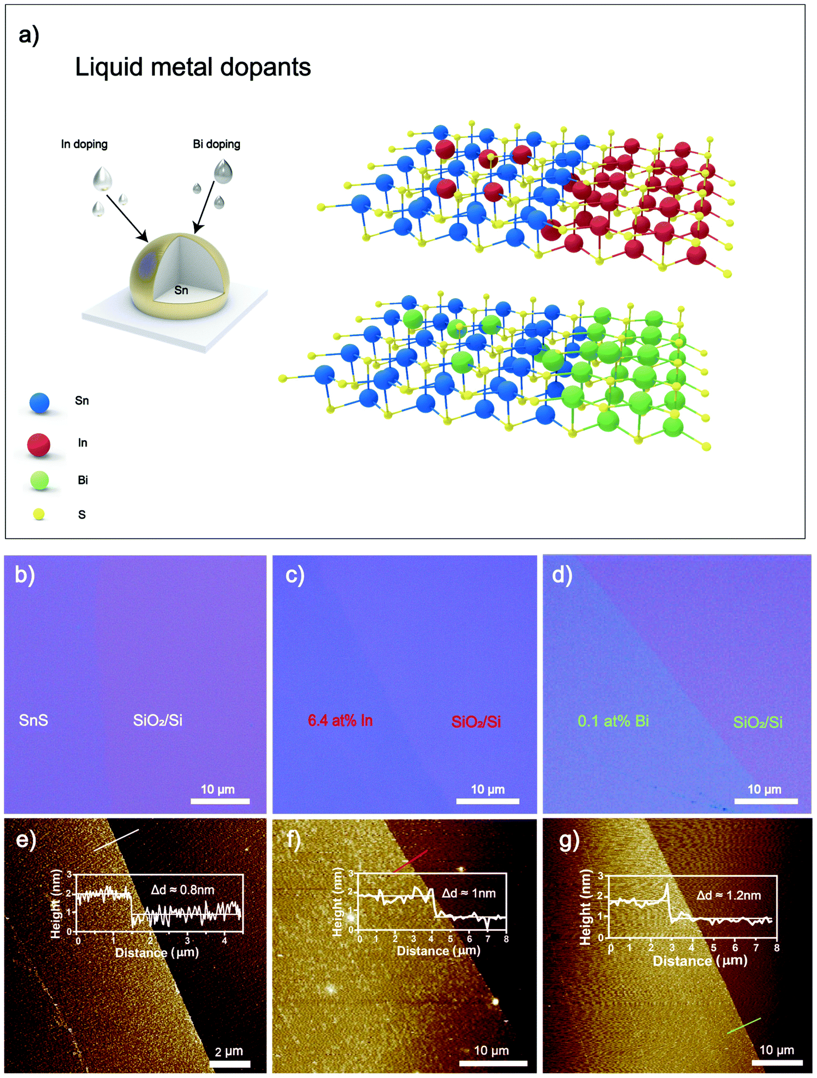 | ||
| Fig. 1 (a) The schematic diagram illustrates the transfer of the 2D SnS nanosheet to the SiO2/Si substrate by the mixed alloy (wt%) through the van der Waals touch printing method. (b–d) Optical images of undoped, 6.4 at% In and 0.1% Bi doped 2D SnS, respectively. The color contrast between the nanosheet and SiO2/Si substrates can be clearly observed. (e–g) AFM topography and height profile illustrates the film thickness corresponding to b–d. The height profiles along the white (e), red (f) and green (g) lines overlaid on the images. | ||
Large area (i.e., hundreds of micrometers), doped 2D SnS nanosheets were then obtained by van der Waals transfer to the substrate. Optical images in Fig. 1b–d elucidate the smooth and uniform transferred 2D sheets of the pristine, In and Bi-doped SnS onto the SiO2/Si substrates, respectively. Atomic force microscopy (AFM) is used to characterize the thickness of the transferred 2D nanosheets. The thickness of pristine 2D SnS nanosheets is measured as 0.8 nm (Fig. 1e). In doped 2D sheets were measured to be 1.0 nm thick (Fig. 1f), and Bi doped 2D sheets were measured at 1.2 nm thick (Fig. 1g), correlating to the greater atom size of In and Bi respectively.
X-ray photoelectron spectroscopy (XPS) is used to analyze the atomic composition of doped 2D SnS (Fig. 2a–d, ESI Fig. S2 and S3†). The XPS results in Fig. 2b show the binding energies of Bi cations and the Bi 4f7/2 peak is located at 158.5 eV and Bi 4f5/2 peak is located at 163.7 eV.35 The In-doped sample in Fig. 2d shows the In 3d5/2 peak situated at 444.8 eV and the In 3d3/2 peak which is situated at 452.4 eV.36 No metallic state of the Bi and In was observed in the printed 2D SnS, suggesting the existence of these atoms in the crystal structure as the cations. The Sn 3d5/2 peak of Sn in 2D SnS is located at 486.5 eV and Sn 3d3/2 peak is located at 494.9 eV, representing the oxidation state of SnS.4,8 The Bi:Sn alloy concentration was incrementally changed from 25, 50, 75 to 90 wt%, where the 90% Bi:Sn alloy had the highest Bi-doping concentration of 0.6 at% in the 2D nanosheets. In comparison, as the In:Sn alloy concentration ratio increased, from 0.1, 0.3, 0.6, to 0.9 wt%, the In-doping significantly increased to 17 at% 2D nanosheets from the In:Sn alloy of 0.9 wt%. The detailed XPS analysis results are presented in the ESI Fig. S2 and S3.†
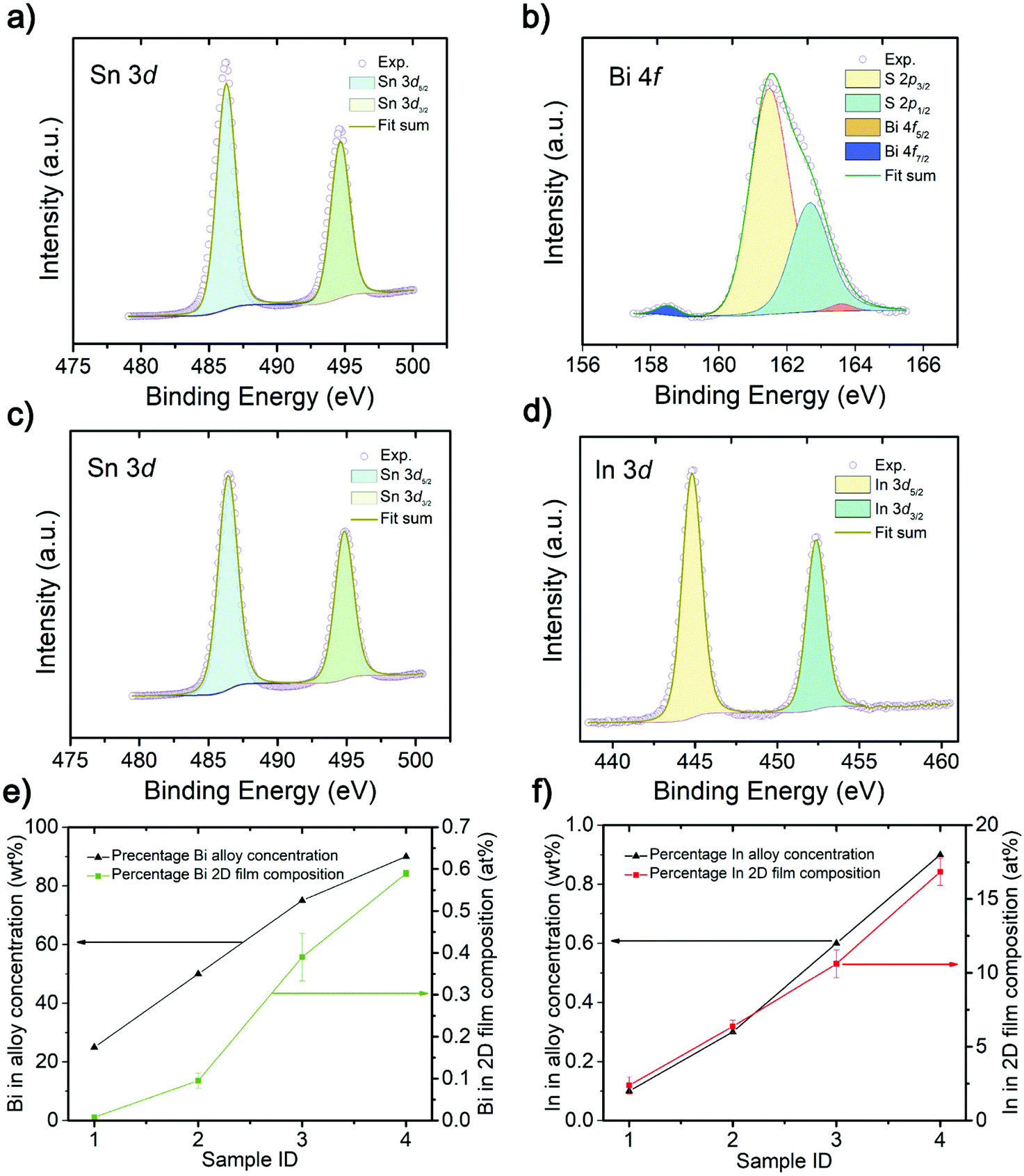 | ||
| Fig. 2 (a) The Sn XPS spectra of 0.1 at% Bi doped in SnS nanosheet (Sn 3d5/2 and Sn 3d3/2). (b) The Bi XPS spectra of 0.1 at% Bi doped in SnS nanosheet (Bi 4f7/2 and Bi 4f5/2). (c) The Sn XPS spectra of 6.4 at% In doped in SnS nanosheet (Sn 3d5/2 and Sn 3d3/2) (d) The In3+ XPS spectra of 6.4 at% In doped in SnS nanosheet (In 3d5/2 and In 3d5/2). (e) Quantitative measurement of 2D doped Bi3+ (0, 0.1, 0.4 and 0.6 at%) obtained from alloys mixed with different weight ratios of 25, 50, 75 and 90 wt% from left to right. The error bars represent the standard errors of the doping ratios of four different measurements. (f) Quantitative measurement of the 2D doping of In3+ (2.4, 6.4, 11 and 17 at%) obtained from alloys mixed with different weight ratios of 0.1, 0.3, 0.6 and 0.9 wt%. The error bars represent the standard errors of the doping ratios of four different measurements. | ||
High-resolution transmission electron microscopy (HRTEM) was used to analyze crystal structure and atomic spacings (Fig. 3). 2D samples were printed directly on holey carbon grids. Doping had resulted in the generation of grain boundaries of In2S3 and Bi2S3 as shown in Fig. 3e and f. Interestingly, the boundaries are connected through an interface between 2D SnS and In2S3 and Bi2S3 grains that are void from breakages and damage, confirming a smooth 2D formation observed from optical and AFM measurements as seen in Fig. 1. The sulphide crystal structure for In2S3 and Bi2S3 are consistent with previously reported liquid metal obtained 2D sulphides.37,38
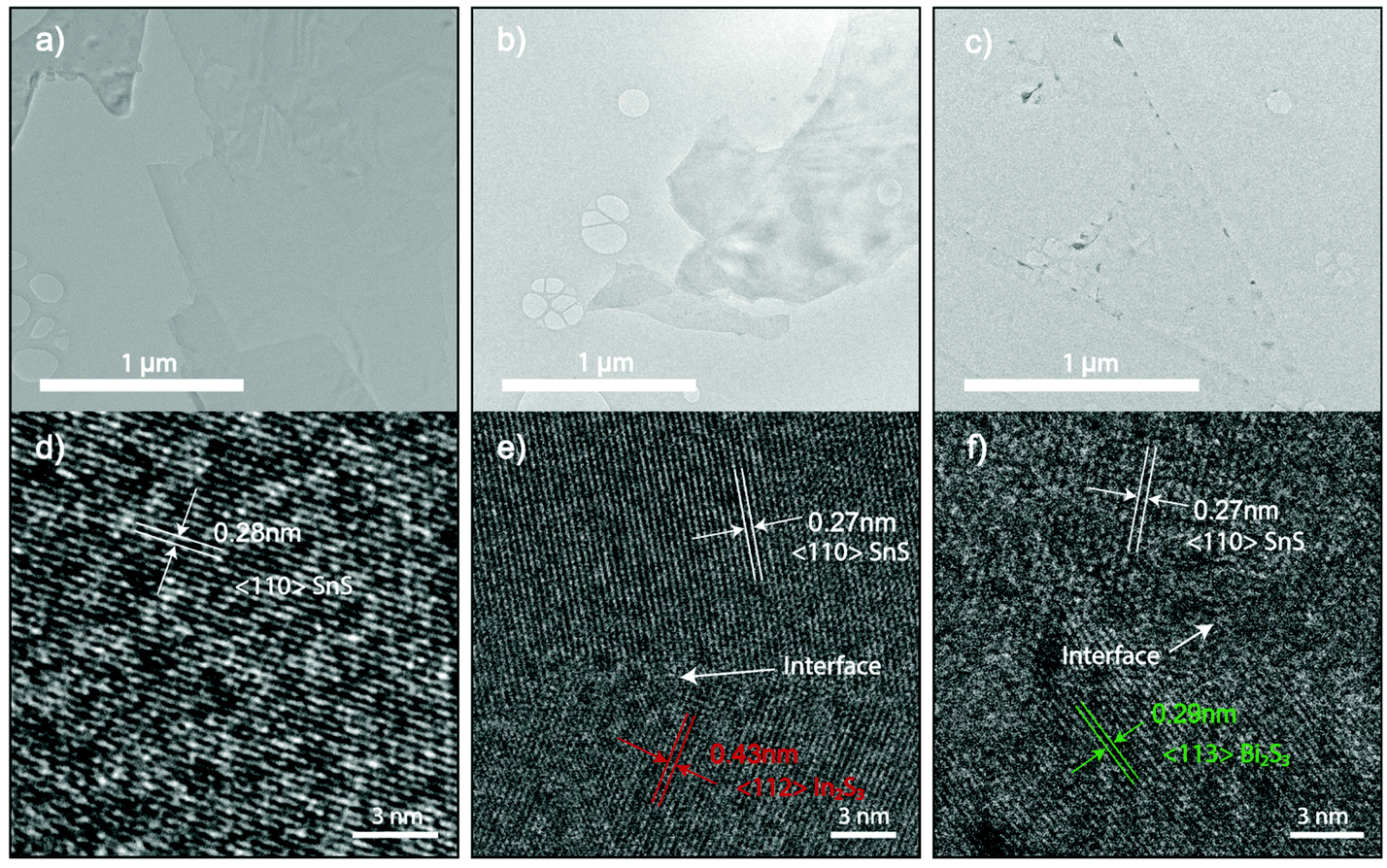 | ||
| Fig. 3 (a–c) The bright-field TEM image of undoped 2D SnS and 6.4 at% In and 0.1% Bi doped 2D SnS, respectively. (d–e) HRTEM images of the corresponding TEM images in a–c showing the formation of In2S3 and Bi2S3 grains. The sulfide doping formation is in agreement with the oxide counterpart.22 | ||
The optoelectronic properties of pristine 2D SnS has been demonstrated, showing ultrafast photodetection responses of 22 μs.4 The photoresponse measurement of Bi-doped 2D SnS was performed at room temperature by irradiating monochromatic light on a device with a 100 μm active area (Fig. 4a and b). Fig. 4c shows the variation of the photocurrent DIph (DIph = Illumination − Idark) with different wavelengths when the illumination power density is 2 mW cm−2 under a 0.5 V applied bias. The DIph value is the highest at 365 nm. It can be observed that light with a wavelength of 365 nm has the strongest effect on the generation of photoexcited carriers. With an increase of wavelength, the energy of light decreases, so the generation of photoexcited carriers also decreases at 1050 nm. Fig. 4d shows the rise and fall times under the irradiation of the wavelength that produces the most photoactive carriers. For the 365 nm wavelength irradiation, the rise time is about 1.9 s. This rise time is significantly longer than that of the previous experiment by Krishnamurthi et al. (ESI Fig. S4†),4 where the rise time of the 2D SnS film is ∼22 μs.
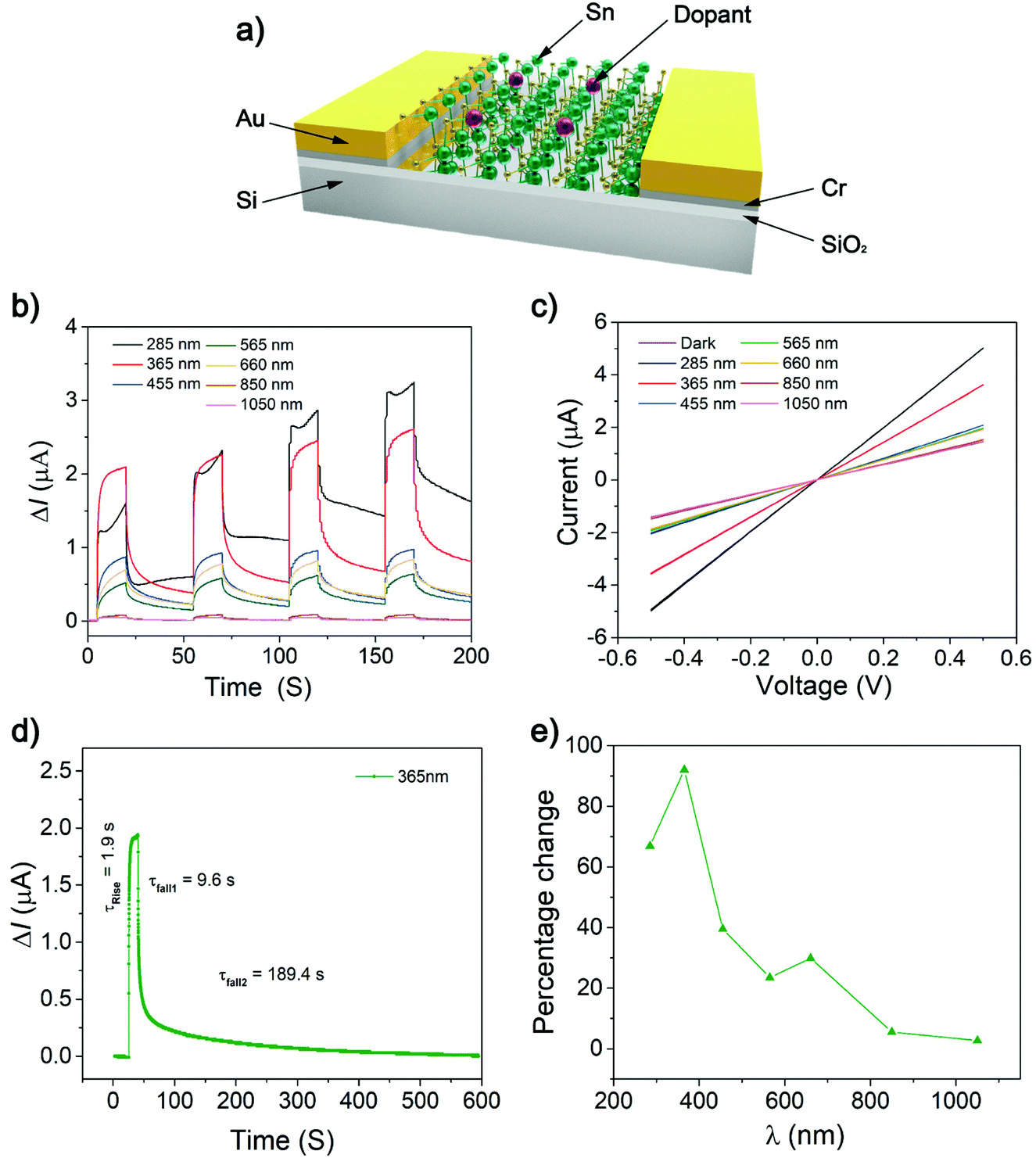 | ||
| Fig. 4 (a) Schematic diagram of the optoelectronic performance device. (b) Photocurrent at different wavelengths for a single layer of 0.1 at% Bi doping SnS. (c) Photocurrent (DIph) of different monochromatic lights with different wavelengths in the static voltage bias from −0.5 V to +0.5 V, including dark conditions. (d) The response time of 0.1 at% Bi-doped 2d SnS nanosheet at a wavelength of 285 nm and a frequency of 500 Hz measured between 10% and 90% of the step height. (e) The photocurrent changes by ratio obtained at different wavelengths at Pinc = 2 mW cm−2 and Vds = 0.5 V for a single layer of 0.1 at% Bi-doped in SnS nanosheet. | ||
Similarly, the fall time of this experiment is 9.6–189.4 s, which is much longer than the fall time of the undoped 2D SnS film of 51 μs.4 The experimental results reveal a slow rise and decay which can be associated with grain boundary generation. Fig. 4e mainly shows DIph relative to the baseline under the excitation of different wavelengths of light. It can be clearly observed that the 365 nm wavelength light changes the photocurrent DIph the most, which is close to 92%. With the wavelength increasing, the change amplitude of the photocurrent DIph decreases correspondingly. The rate of decrease at 565 nm and 660 nm consequently maintains a change of 25% and finally drops to about 5% at 1050 nm wavelength light. The results of such photodetectors are substantially different from Krishnamurthi et al.4 The photocurrent generation has longer fall times from non-doped of 22 μs (ref. 4) to Bi-doped of 189.4 s (Fig. 4d and ESI Fig. S4a†). The long exciton lifetime is due to crystal grain formations leading to increased exciton trappings, augmenting the relaxation pathways. This phenomenon has been reported in doped tin sulfide compounds using Na,39 In,40 Sb28 and Al.41
Group IV monochalcogenides (MX, M – Sn or Ge, X – Se or S), namely SnSe, SnS, GeSe and GeS, has recently become an emerging area for piezoelectric research featuring stable non-centrosymmetric crystals.42 Secondly, their puckered C2v symmetry is more flexible (softer) in the armchair direction, further enhancing the piezoelectric effect.43 2D SnS nanosheets have been simulated by first-principles density functional theory (DFT) to calculate the piezoelectric coefficients. The d11 coefficient has been calculated to be two orders of magnitude larger than those of other 2D materials and bulk materials.14Fig. 5a shows the morphology of the synthesized 2D SnS with a thickness of ∼1 nm. Fig. 5b, c and ESI Fig. S5† show the results of the lateral piezoelectric effect and phase of the In-doped 2D SnS. For benchmarking, the comparison of In-doped and pristine 2D SnS and periodically polarized lithium niobate (PPLN) reference sample with the lateral piezoelectric response are shown in Fig. 5d. The results of these three samples show that with the increase of the driving voltage, the piezoelectric response illustrates a linear increase. The slope of the linear fitting line can be used to calculate the effective piezoelectric coefficient. The doped and pristine 2D SnS and the reference PPLN sample have relative slopes of 1:0.6:0.16, respectively. Since the lateral direction of PPLN deff = 5.92 pm V−1 (ESI Fig. S6†), the In-doped single-layer SnS can be calculated, the effective piezoelectric coefficient is 37.5 pm V−1. Khan et al. found the piezoelectric response of pristine 2D SnS as is 26 pm V−1.8 Compared with pristine (ESI Fig. S7†), the piezoelectric response of In-doped 2D SnS is remarkably increased by ∼22.6%. However, in contrast, Bi doping has quenched the piezoresponse of the material (ESI Fig. S5 and S8†). This quenched response demonstrates clearly that there is negligible substrate effect and no artifacts from contact electrification in the PFM data.44 It is thought that the large atom size of Bi should increase asymmetry in the SnS crystal structure, so further studies and theoretical interpretation are needed to understand why there is zero piezoelectric response.
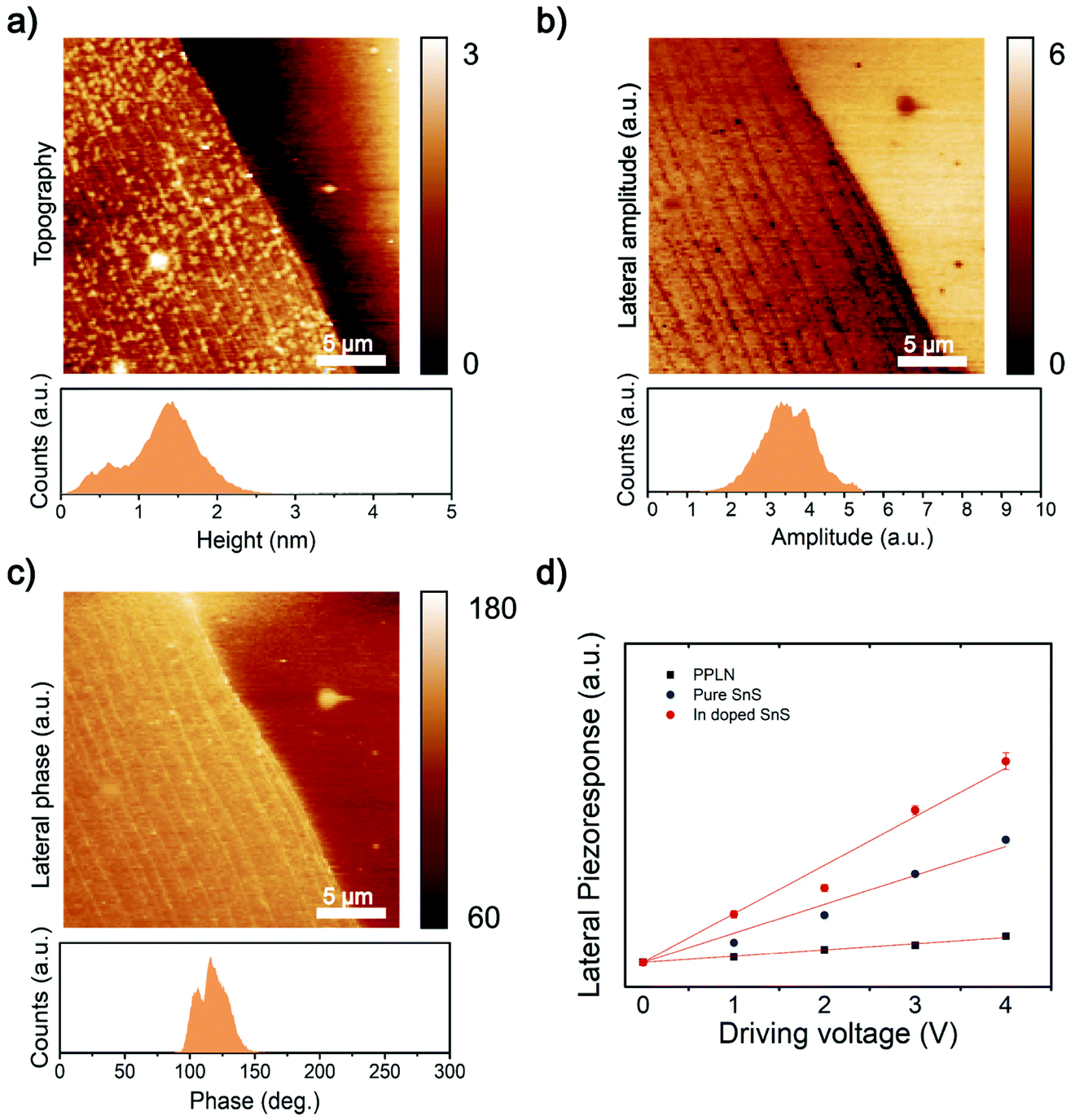 | ||
| Fig. 5 2D SnS with 6.4 at% In doping lateral piezoelectric response. (a) The AFM morphology and the 2D layer. (b) 6.4 at% In alloy concentration single layer Lateral amplitude, histogram with the attached picture. (c) 6.4 at% In doped in SnS lateral phase, the inset is a histogram. (d) The lateral piezoelectric response of 6.4 at% In doped in SnS single layer nano-film, pristine and PPLN to different driving voltages. Error bars indicate the standard deviation of the measurement. | ||
3. Conclusions
Engineering 2D materials is a promising pathway to fully exploit their potential. Liquid metals offer a novel platform for obtaining unique 2D materials and enable the manipulation of 2D compositions. In this work, liquid metal methods are used to dope 2D SnS based on the selective migration mechanism.22 We selected Bi and In due to the potential formation of substitutional alloy and the low melting point of the base metals. For comparing Gibbs free energy (ΔGf) of reaction for the formation of In2S3, SnS and Bi2S3 the normalized energy based on the unit-mole of the reactant was calculated. The normalized energies were −165, −98.3 and −56.24 (kJ mol−1) respectively.45 The more negative ΔGf represents the higher reactivity. Therefore the metal dopants have been selected accordingly so that the 2D sheets are dominated by SnS.The liquid metal doping of In in 2D SnS has shown a substantial 22.6% increase in piezoelectric coefficient achieved at 6.4 at% In:Sn. This is due to the doping effect on augmenting the polarization. In addition, broadband photodetection performance of doped SnS was analyzed. The high-energy photon wavelength of 365 nm excites the maximum number of electrons located in the valence band to the high-energy conduction band allowing the practical analysis of the response times. The response time is affected by carrier transition time during the recombination, in which several defects and consequently spacially isolated potential barriers prolong the recombination equilibrium. The response time was increased by several orders rendering a significant carrier lifetime compared with the pristine 2D SnS, which can aid in realising applications for neuromorphics. These results suggest a vast opportunity for tuning and engineering 2D nanosheets for optoelectronics performances using the liquid metal approach.
4. Experimental
4.1. Materials
Tin (Sn, 99.8%), bismuth (Bi, 99.98%) and indium (In, 99.99%) were purchased from Roto Metals. All other reagents and solvents were obtained from Sigma-Aldrich and used according to the received standards.4.2. Liquid metal alloy preparation
One-step touch printing uses van der Waals force to exfoliate the doped 2D SnS film. Firstly, the pre-alloy is obtained by configuring different weight ratios of Bi/Sn and In/Sn. The weight ratios of Bi/Sn of the alloy are 25 wt%, 50 wt%, 75 wt% and 90%, and the weight ratios of In/Sn of the alloy are 0.1%, 0.3%, 0.6% and 0.9%, respectively. After these alloys are weighed by a digital scale, they are transferred to a glove box filled with N2. The O2 concentration in the glove box is strictly controlled. These mixed metals are placed in a glass bottle. Through the heating plate in the glove box, these metals were heated over 300 °C and thoroughly mixed, and then the bottle is removed from the heating plate and cooled naturally to a solid, ready for the next reaction in the H2S environment.The touch printing of doping 2D SnS nanosheet is carried out in a small glove box. In order to exhaust all O2 gas in the chamber, N2 with a flow rate of 500 sccm is pumped into the chamber for more than two hours and then switched to 50 ppm of H2S gas, which is pumped into the chamber at a flow rate of 500 sccm for an hour, so that the small glove box is filled with H2S gas. The pre-mixed alloy is placed on a glass slide, and the glass slide is heated to 350 °C, at this time, the solid metal has melted into a shiny metal ball, but the surface of the silver-white metal ball will gradually turn yellow-brown in the H2S atmosphere, which means that the SnS layer has been formed. At this time, the pre-heated SiO2/Si substrate is ready for printing.
4.3. 2D characterization
The optical image is obtained by using Leica DM2500 optical microscope to observe the In and Bi doped SnS nanosheets on 300 nm SiO2/Si substrates, and the surface morphology image is measured by a Bruker Dimension Icon atomic force microscope (AFM) in ScanAsyst-air mode, and Gwyddion 2.55 software is used to analyze the thickness distribution and surface morphology of 2D nanosheets. The crystal phase analysis is carried out by using JEOL JEM-2100F microscope operating at 200 kV acceleration voltage to obtain low/high-resolution TEM imaging and selected area electron diffraction images. The 2D nanosheets are transferred to the substrate by touch printing with holey Au–Carbon grids (ProScitech, Australia). The analysis of elemental composition is performed using Thermo Scientific K-alpha XPS spectrometer with 1486.7 eV (Al Kα) X-ray source. The CasaXPS software is used for data analyses.4.4. Piezoresponse force microscopy
The characteristics of piezoelectric properties are measured using MFP-Infinity (Oxford Instrument, Asylum Research, Santa Barbara, CA, USA) equipment in the lateral piezoresponse force microscopy (LPFM) mode. The sample chip is interfaced on the magnetic metal piece with double-sided tape, and put the sample with the magnetic metal piece on the metal base together. In order to ensure the accuracy of the piezoelectric results, we pre-measured Asylum Research periodically polarized lithium niobate (AR-PPLN) standard samples to calculate the piezoelectric coefficient deff of the PPLN, so it can be calibrated with the known coefficient pristine and In-doped SnS.4.5. Device fabrication and measurement
The 2D SnS nanosheet is transferred to a 300 nm SiO2/conductive silicon substrate, and then coated with AZ-5214E photoresist. The designed interdigital electrode is patterned by a maskless aligner – Heildberg MLA150, and the AZ-726 MIF Developer is used to flush the pattern scanned by the laser. The PVD75 Kurt J. Lesker electron beam evaporator is used to deposit Cr/Au (10/100 nm) electrodes on the 2D nanosheet. For photoelectric measurement, a commercial monochromatic light emitting diode (Thorlabs, Inc.) is used as the excitation source with a wavelength range of 280–1050 nm. All measurements are carried under dark ambient environment. Illumination power is calibrated by UV-enhanced photodetectors (Newport Corporation). The laser is irradiated on the nanosheet from top to bottom, and the power intensity is fixed at 2 mW cm−2 for varies wavelengths ranging between 280 nm to 1050 nm.Author contributions
X. G., Y. W., J. Y., Y. L. and A. Z. conceptualized the project; X. G., Y. W., and A. E. performed piezoelectric measurements; X. G., A. M. performed photodetection characterizations; C. K. N. conducted UV-Vis measurements, X. G. and V. K. performed materials synthesis and device fabrication; X. G., Y. W. and Y. L. performed materials characterizations; and validation; All other authors have contributed to writing, review & editing; Y. L. and A. Z. performed supervision.Conflicts of interest
There are no conflicts to declare.Acknowledgements
We acknowledge the scientific and technical assistance from RMIT Microscopy & Microanalysis Facility (RMMF) and Micro-Nano Research Facility (MNRF) at RMIT University. The project was funded by the Australian Research Council (ARC) Discovery Project (DP180102752).PCS acknowledges support through the Elizabeth & Vernon Puzey Foundation.
S. W. and Y. L. acknowledge support from the Australian Research Council (DP220100020).
References
- R. Mas-Balleste, C. Gomez-Navarro, J. Gomez-Herrero and F. Zamora, Nanoscale, 2011, 3, 20–30 RSC.
- K. Khan, A. K. Tareen, M. Aslam, R. Wang, Y. Zhang, A. Mahmood, Z. Ouyang, H. Zhang and Z. Guo, J. Mater. Chem. C, 2020, 8, 387–440 RSC.
- B. Mukherjee, Y. Cai, H. R. Tan, Y. P. Feng, E. S. Tok and C. H. Sow, ACS Appl. Mater. Interfaces, 2013, 5, 9594–9604 CrossRef CAS PubMed.
- V. Krishnamurthi, H. Khan, T. Ahmed, A. Zavabeti, S. A. Tawfik, S. K. Jain, M. J. S. Spencer, S. Balendhran, K. B. Crozier, Z. Li, L. Fu, M. Mohiuddin, M. X. Low, B. Shabbir, A. Boes, A. Mitchell, C. F. McConville, Y. Li, K. Kalantar-Zadeh, N. Mahmood and S. Walia, Adv. Mater., 2020, 32, e2004247 CrossRef PubMed.
- J. Lu, C. Nan, L. Li, Q. Peng and Y. Li, Nano Res., 2012, 6, 55–64 CrossRef.
- C. Zhang, H. Yin, M. Han, Z. Dai, H. Pang, Y. Zheng, Y.-Q. Lan, J. Bao and J. Zhu, ACS Nano, 2014, 8, 3761–3770 CrossRef CAS PubMed.
- L. D. Zhao, S. H. Lo, Y. Zhang, H. Sun, G. Tan, C. Uher, C. Wolverton, V. P. Dravid and M. G. Kanatzidis, Nature, 2014, 508, 373–377 CrossRef CAS PubMed.
- H. Khan, N. Mahmood, A. Zavabeti, A. Elbourne, M. A. Rahman, B. Y. Zhang, V. Krishnamurthi, P. Atkin, M. B. Ghasemian, J. Yang, G. Zheng, A. R. Ravindran, S. Walia, L. Wang, S. P. Russo, T. Daeneke, Y. Li and K. Kalantar-Zadeh, Nat. Commun., 2020, 11, 3449 CrossRef CAS PubMed.
- Y. Guo, S. Zhou, Y. Bai and J. Zhao, ACS Appl. Mater. Interfaces, 2017, 9, 12013–12020 CrossRef CAS PubMed.
- H. Wang and X. Qian, 2D Mater., 2017, 4(1), 015042 CrossRef.
- J. R. Brent, D. J. Lewis, T. Lorenz, E. A. Lewis, N. Savjani, S. J. Haigh, G. Seifert, B. Derby and P. O'Brien, J. Am. Chem. Soc., 2015, 137, 12689–12696 CrossRef CAS PubMed.
- C. Xin, J. Zheng, Y. Su, S. Li, B. Zhang, Y. Feng and F. Pan, J. Phys. Chem. C, 2016, 120, 22663–22669 CrossRef CAS.
- L. C. Gomes, A. Carvalho and A. H. Castro Neto, Phys. Rev. B: Condens. Matter Mater. Phys., 2015, 92(21), 214103 CrossRef.
- R. Fei, W. Li, J. Li and L. Yang, Appl. Phys. Lett., 2015, 10(17), 173104 CrossRef.
- P. Luo, F. Zhuge, Q. Zhang, Y. Chen, L. Lv, Y. Huang, H. Li and T. Zhai, Nanoscale Horiz., 2019, 4, 26–51 RSC.
- Z. Hu, Z. Wu, C. Han, J. He, Z. Ni and W. Chen, Chem. Soc. Rev., 2018, 47, 3100–3128 RSC.
- W. Liao, S. Zhao, F. Li, C. Wang, Y. Ge, H. Wang, S. Wang and H. Zhang, Nanoscale Horiz., 2020, 5, 787–807 RSC.
- W. Shin, S. Hong, Y. Jeong, G. Jung, J. Park, D. Kim, C. Lee, B. G. Park and J. H. Lee, Nanoscale, 2021, 13, 9009–9017 RSC.
- V. Van On, D. K. Nguyen, J. Guerrero-Sanchez and D. M. Hoat, New J. Chem., 2021, 45, 20776–20786 RSC.
- Z. Wang, H. Kannan, T. Su, J. Swaminathan, S. N. Shirodkar, F. C. Robles Hernandez, H. C. Benavides, R. Vajtai, B. I. Yakobson, A. Meiyazhagan and P. M. Ajayan, Nanoscale Adv., 2021, 3, 1747–1757 RSC.
- Y. Gong, H. Yuan, C. L. Wu, P. Tang, S. Z. Yang, A. Yang, G. Li, B. Liu, J. van de Groep, M. L. Brongersma, M. F. Chisholm, S. C. Zhang, W. Zhou and Y. Cui, Nat. Nanotechnol., 2018, 13, 294–299 CrossRef CAS PubMed.
- M. B. Ghasemian, A. Zavabeti, M. Mousavi, B. J. Murdoch, A. J. Christofferson, N. Meftahi, J. Tang, J. Han, R. Jalili, F. M. Allioux, M. Mayyas, Z. Chen, A. Elbourne, C. F. McConville, S. P. Russo, S. Ringer and K. Kalantar-Zadeh, Adv. Mater., 2021, 33, e2104793 CrossRef PubMed.
- A. Dussan, F. Mesa and G. Gordillo, J. Mater. Sci., 2010, 45, 2403–2407 CrossRef CAS.
- K. Norton, J. Kunstmann, L. Ping, A. Rakowski, C. Wang, A. J. Marsden, G. Murtaza, N. Zeng, S. G. McAdams, S. J. McAdams, M. A. Bissett, S. J. Haigh, B. Derby, G. Seifert, J. C. Ke and D. J. Lewis, Chem. Sci., 2019, 10, 1035–1045 RSC.
- F. Y. Ran, Z. Xiao, Y. Toda, H. Hiramatsu, H. Hosono and T. Kamiya, Sci. Rep., 2015, 5, 10428 CrossRef PubMed.
- M. Patel and A. Ray, RSC Adv., 2014, 4, 39343–39350 RSC.
- H. Kafashan, Mater. Res. Express, 2018, 5(4), 046417 CrossRef.
- M. Seal, N. Singh, E. W. McFarland and J. Baltrusaitis, J. Phys. Chem. C, 2015, 119, 6471–6480 CAS.
- S. Sebastian, I. Kulandaisamy, A. M. S. Arulanantham, S. Valanarasu, A. Kathalingam, M. Shkir and S. AlFaify, Rare Met., 2022, 41, 1661–1670 Search PubMed.
- S. Zhang, S. Cheng, H. Jia and H. Zhou, Adv. Mater. Res., 2011, 418–420, 712–716 Search PubMed.
- S. Sebastian, I. Kulandaisamy, S. Valanarasu, N. Soundaram, K. Paulraj, D. Vikraman and H.-S. Kim, J. Mater. Sci.: Mater. Electron., 2019, 30, 8024–8034 CrossRef CAS.
- Z. Wang, L. Huang, C. Zhang, M. Chuai, X. Zhang and M. Zhang, J. Alloys Compd., 2019, 799, 425–432 CrossRef CAS.
- S. Sebastian, S. Vinoth, K. H. Prasad, M. S. Revathy, S. Gobalakrishnan, P. K. Praseetha, V. Ganesh and S. AlFaify, Appl. Phys. A, 2020, 126(10), 1–12 CrossRef.
- A. Zavabeti, J. Z. Ou, B. J. Carey, N. Syed, R. Orrell-Trigg, E. L. H. Mayes, C. Xu, O. Kavehei, A. P. O'Mullane, R. B. Kaner, K. Kalantar-zadeh and T. Daeneke, Science, 2017, 358, 332–335 CrossRef CAS PubMed.
- T. J. Whittles, L. A. Burton, J. M. Skelton, A. Walsh, T. D. Veal and V. R. Dhanak, Chem. Mater., 2016, 28, 3718–3726 CrossRef CAS.
- L. A. H. Jones, W. M. Linhart, N. Fleck, J. E. N. Swallow, P. A. E. Murgatroyd, H. Shiel, T. J. Featherstone, M. J. Smiles, P. K. Thakur, T.-L. Lee, L. J. Hardwick, J. Alaria, F. Jäckel, R. Kudrawiec, L. A. Burton, A. Walsh, J. M. Skelton, T. D. Veal and V. R. Dhanak, Phys. Rev. Mater., 2020, 4(7), 074602 CrossRef CAS.
- A. Jannat, Q. Yao, A. Zavabeti, N. Syed, B. Y. Zhang, T. Ahmed, S. Kuriakose, M. Mohiuddin, N. Pillai, F. Haque, G. Ren, D. M. Zhu, N. Cheng, Y. Du, S. A. Tawfik, M. J. S. Spencer, B. J. Murdoch, L. Wang, C. F. McConville, S. Walia, T. Daeneke, L. Zhu and J. Z. Ou, Mater. Horiz., 2020, 7, 827–834 RSC.
- K. A. Messalea, A. Zavabeti, M. Mohiuddin, N. Syed, A. Jannat, P. Atkin, T. Ahmed, S. Walia, C. F. McConville, K. Kalantar-Zadeh, N. Mahmood, K. Khoshmanesh and T. Daeneke, Adv. Mater. Interfaces, 2020, 7(22), 2001131 CrossRef CAS.
- B. Ouyang, W. He, L. Wu, L.-D. Zhao and Y. Yang, Nano Energy, 2021, 88, 106268 CrossRef CAS.
- C. Fan, Z. Liu, S. Yuan, X. Meng, X. An, Y. Jing, C. Sun, Y. Zhang, Z. Zhang, M. Wang, H. Zheng and E. Li, ACS Appl. Mater. Interfaces, 2021, 13, 35889–35896 CrossRef CAS PubMed.
- X. Meng, C. Fan, X. An, S. Yuan, Y. Jing, Z. Liu, C. Sun, Y. Zhang, Z. Zhang, M. Wang, H. Zheng and E. Li, CrystEngComm, 2021, 23, 4694–4699 RSC.
- P. C. Sherrell, M. Fronzi, N. A. Shepelin, A. Corletto, D. A. Winkler, M. Ford, J. G. Shapter and A. V. Ellis, Chem. Soc. Rev., 2022, 51, 650–671 RSC.
- L. Li, Z. Chen, Y. Hu, X. Wang, T. Zhang, W. Chen and Q. Wang, J. Am. Chem. Soc., 2013, 135, 1213–1216 CrossRef CAS PubMed.
- A. Sutka, P. C. Sherrell, N. A. Shepelin, L. Lapcinskis, K. Malnieks and A. V. Ellis, Adv. Mater., 2020, 32, e2002979 CrossRef PubMed.
- W. M. Haynes, Crc Handbook of Chemistry and Physics, CRC Press LLC, Milton, United Kingdom, 2016 Search PubMed.
Footnotes |
| † Electronic supplementary information (ESI) available: It contains information about process, materials characterization, photodetection an piezoelectric measurements. See DOI: https://doi.org/10.1039/d2nr01135b |
| ‡ These authors contributed equally. |
| This journal is © The Royal Society of Chemistry 2022 |