
 Open Access Article
 This Open Access Article is licensed under a Creative Commons Attribution-Non Commercial 3.0 Unported Licence
Halide perovskite single crystals: growth, characterization, and stability for optoelectronic applications
Yunae
Cho
 a,
Hye Ri
Jung
b and
William
Jo
*ab
a,
Hye Ri
Jung
b and
William
Jo
*ab
aNew and Renewable Energy Research Centre, Ewha Womans University, Seoul, Republic of Korea. E-mail: wmjo@ewha.ac.kr
bDepartment of Physics, Ewha Womans University, Seoul, Republic of Korea
First published on 7th June 2022
Abstract
Recently, metal halide perovskite materials have received significant attention as promising candidates for optoelectronic applications with tremendous achievements, owing to their outstanding optoelectronic properties and facile solution-processed fabrication. However, the existence of a large number of grain boundaries in perovskite polycrystalline thin films causes ion migration, surface defects, and instability, which are detrimental to device applications. Compared with their polycrystalline counterparts, perovskite single crystals have been explored to realize stable and excellent properties such as a long diffusion length and low trap density. The development of growth techniques and physicochemical characterizations led to the widespread implementation of perovskite single-crystal structures in optoelectronic applications. In this review, recent progress in the growth techniques of perovskite single crystals, including advanced crystallization methods, is summarized. Additionally, their optoelectronic characterizations are elucidated along with a detailed analysis of their optical properties, carrier transport mechanisms, defect densities, surface morphologies, and stability issues. Furthermore, the promising applications of perovskite single crystals in solar cells, photodetectors, light-emitting diodes, lasers, and flexible devices are discussed. The development of suitable growth and characterization techniques contributes to the fundamental investigation of these materials and aids in the construction of highly efficient optoelectronic devices based on halide perovskite single crystals.
1. Introduction
Metal halide perovskite materials have recently garnered significant attention owing to their attractive optical, electronic, and optoelectronic properties such as high absorption coefficients,1,2 direct bandgaps, long carrier lifetime,3–5 high mobility,6 low costs,7 and facile deposition techniques.8 In general, the perovskites are represented by the structure—ABX3 (A = CH3NH3+, H2NCHNH2+, Cs+; B = Pb2+, Sn2+; X = Cl−, Br−, I−), as shown in Fig. 1a.9 In the past decade, the photovoltaic properties of metal halide perovskites have been studied extensively, and a remarkable efficiency of 25.8% (certified 25.7%) has been reportedly achieved using such materials.10,11 However, the chemical and structural instability of the perovskites remains a major obstacle that hinders their widespread application in various fields.12 To evaluate the stability of the perovskites, a tolerance factor (t) has been proposed as: t = (RA + RX)/√2(RM + RX), where RA, RM, and RX represent the ionic radii of the ions occupying the A, M, and X sites, respectively.13 The knowledge of the tolerance factor of a perovskite helps us to investigate its unusual and novel properties. In general, the t factor ranges from 0.7 to 1.0 for halogen-based perovskites, as shown in Fig. 1b.14 For most cubic perovskites with perfectly packed structures, t varies from 0.9 to 1, although a slight variation in this range may be observed for distorted structures.15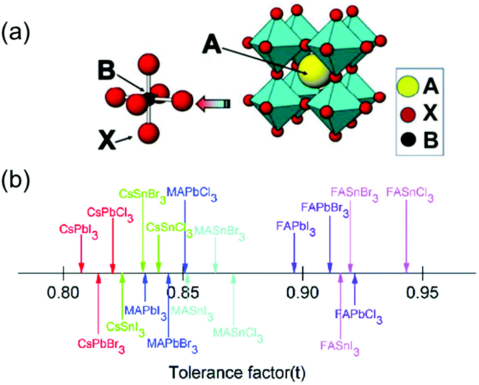 | ||
| Fig. 1 (a) Cubic crystal structure of an ABX3 perovskite with common substituents listed for the A, B, and X positions (A = MA+, FA+, Cs+etc.; B = Pb2+, Sn2+, etc.; X = Cl−, Br−, or I−). Reproduced with permission.9 Copyright 2018, MDPI. (b) Tolerance factors (t) of a series of metal halide perovskites. Reproduced with permission.14 Copyright 2018, RSC. | ||
Fig. 2 shows the relationship between the lattice constant and bandgap of polycrystalline and single-crystalline perovskites, along with the visible light range.16 The lattice matching of these materials indicates that they can be used to form heterojunctions for novel multi-structured applications like tandem devices.17 Further, understanding the relationship between the lattice constant and bandgap helps bandgap engineering and facilitates feasible applications in the visible light range because, based on such an understanding, various perovskite candidates for specific applications can be engineered easily, as shown in Fig. 2.18–24 Most reported perovskite devices based on polycrystalline thin films exhibit poor stability and high trap densities created by grain boundaries,12 which severely limit their performance. Reportedly, perovskite single crystals show superior properties such as longer carrier diffusion lengths, lower trap-state densities, and better stability, compared with their polycrystalline thin-film counterparts.5,25–34 These outstanding properties have promoted a wide range of applications of perovskite single crystals in solar cells,29,31,35–38 photodectors,32–34,39–42 light-emitting diodes (LEDs),43–45 lasers,46–48 and flexible electronic devices.49–52
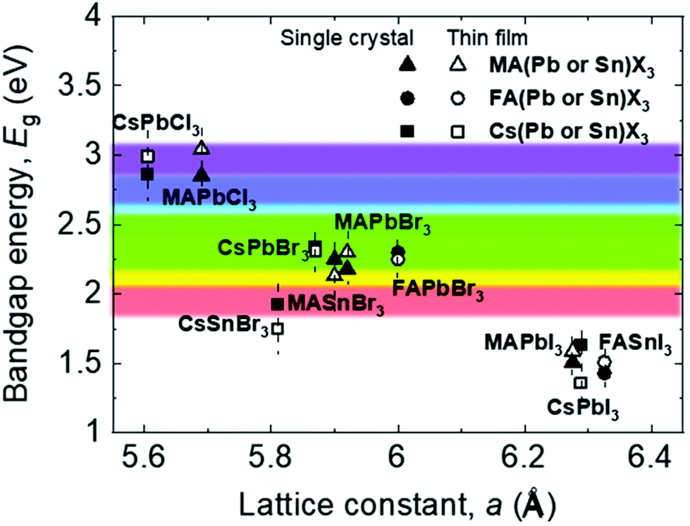 | ||
| Fig. 2 Relationship between the bandgap energy and lattice constant of perovskite single crystals and thin films. | ||
This review article has been presented with the aim to trace the technical development of metal halide perovskite single crystals and provide new ideas on their potential applications. First, we summarize the vast range of growth techniques that have been implemented for the fabrication of single-crystal perovskites with up-to-date quality control. Second, the fundamental physicochemical characteristics of metal halide perovskite single crystals have been intensively summarized, including their optical behaviors, charge carrier transport, and electronic properties. In addition, to overcome the stability issues of perovskite single crystals, better properties than those of polycrystalline films are introduced and further improvements are described.53–57 Promising applications of perovskite single crystals are highlighted as well. Finally, the scientific challenges and strategies for potential applications are discussed.
2. Growth techniques
In this section, the typical and promising growth techniques of perovskite single crystals are summarized. These methods can be divided into two categories, viz. conventional solution growth and promising growth with advanced quality control. In the following sections, these growth techniques for single crystals are classified according to the principle of synthesis, and additional controls for mixed compounds as well as those for fast- and thin-crystal growth are discussed.2.1. Conventional solution growth
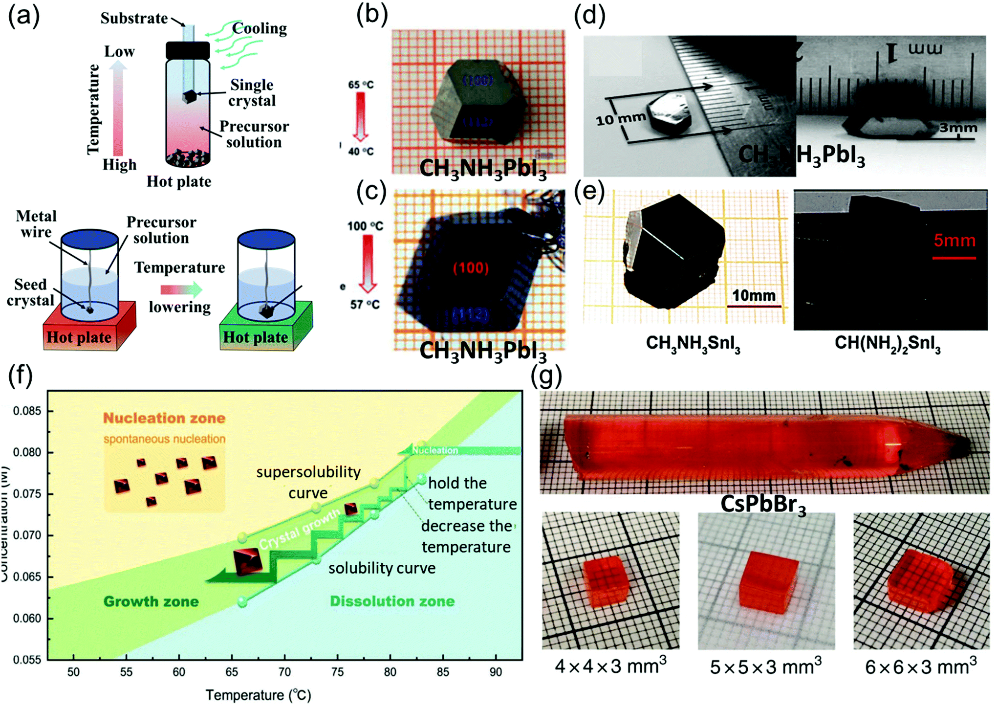 | ||
| Fig. 3 (a) Schematic illustration of the basic principle and single crystals prepared via low-temperature crystallization. (b) MAPbI3 single crystals prepared by low-temperature crystallization. Reproduced with permission.59 Copyright 2015, RSC. (c) Centimeter-sized MAPbI3 single crystals prepared by low-temperature crystallization. Reproduced with permission.60 Copyright 2015, Springer Nature. (d) MASnI3 single crystals. Reproduced with permission.5 Copyright 2015, AAAS. (e) FASnI3 single crystals. Reproduced with permission.61 Copyright 2019, Wiley-VCH. (f) Temperature-dependent solubility and supersolubility curves for the Cs2AgBiBr6 crystal growth; the nucleation, growth, and dissolution zones are divided by the two curves. Reproduced with permission.45 Copyright 2017, Wiley-VCH. (g) As-grown single-crystal ingot with a diameter of 11 mm, and the single crystal wafers with different sizes. Reproduced with permission.62 Copyright 2018, Springer Nature. | ||
In Poglitsch and Weber's method, MAPbI3 single crystals (size: 10 mm × 10 mm × 8 mm) were successfully grown at the bottom of the flask after several days, when the solution temperature was decreased from 65 to 40 °C as shown in Fig. 3b. These crystals were then washed and filtered with HI and acetone. When the temperature was below 40 °C, yellow needle-like crystals formed, different from the black MAPbI3 crystal.59
Lian et al.60 precisely controlled the temperature gradient to 1 °C h−1 while decreasing the solution temperature from 100 to 57 °C, leading to the formation of MAPbI3 single crystals (size: 12 mm × 12 mm × 7 mm) over 15 days. They used small seed crystals at the end of a platinum wire in the solution as depicted in Fig. 3c.
Dong et al.5 used many small MAPbI3 crystals as the seed crystals, which provided excess MA+, Pb2+, and I− ions to keep the solution saturated. Moreover, a silicon substrate was dipped in the precursor solution, leading to the nucleation of small crystals in several hours. The authors then placed only one large seed on the substrate to induce growth at a crystallization rate of approximate 2 mm day−1, and MAPbI3 single crystals with lateral thicknesses of 10 and 3.3 mm were produced as shown in Fig. 3d. By combining the advantages of the TSSG and BSSG methods, Dang et al.61 also obtained MASnI3 and CH(NH2)2SnI3 (FASnI3) single crystals, as depicted in Fig. 3e. Yin et al.45 employed the supersolubility and solubility curves of Cs2AgBiBr6 to indicate the growth process along with the nucleation, growth, and dissolution zones, as shown in Fig. 3f. He et al.62 reported the optimization of CsPbBr3 single-crystal ingots, each with a diameter of 11 mm and length over 6 cm, through the melt temperature, temperature gradient, and various cooling strategies as shown in Fig. 3e. In this method, initially, CsBr and PbBr2 were directly mixed in a stoichiometric ratio of 1![[thin space (1/6-em)]](https://www.rsc.org/images/entities/char_2009.gif) :1 at 580 °C, and the synthesis was performed in a conical silica tube. The silica tube was heated to a temperature of 590 °C for 10 h, and then maintained at this temperature for 12 h to prevent heterogeneous nucleation of the crystals, as overheating the melt (15–30 K) reduces the surplus nucleation centers. Moreover, the temperature gradient region (5–20 K cm−1) featuring a low dropping speed (0.5–2 mm h−1) employed in various cooling strategies helps in avoiding thermally induced cracks. Next, the prepared ingot was cooled down to 200 °C for 20 h, followed by cooling to room temperature at a rate of 2–5 K h−1, resulting in the growth of CsPbBr3 ingots.
:1 at 580 °C, and the synthesis was performed in a conical silica tube. The silica tube was heated to a temperature of 590 °C for 10 h, and then maintained at this temperature for 12 h to prevent heterogeneous nucleation of the crystals, as overheating the melt (15–30 K) reduces the surplus nucleation centers. Moreover, the temperature gradient region (5–20 K cm−1) featuring a low dropping speed (0.5–2 mm h−1) employed in various cooling strategies helps in avoiding thermally induced cracks. Next, the prepared ingot was cooled down to 200 °C for 20 h, followed by cooling to room temperature at a rate of 2–5 K h−1, resulting in the growth of CsPbBr3 ingots.
22,66,67 and MAPbCl323,39,66,68 single crystals, respectively. This method was initially used for preparing single-crystal perovskites of MAPbX3. However, for synthesizing mixed-halide perovskites, it is still challenging to use one solvent for both the precursor materials.
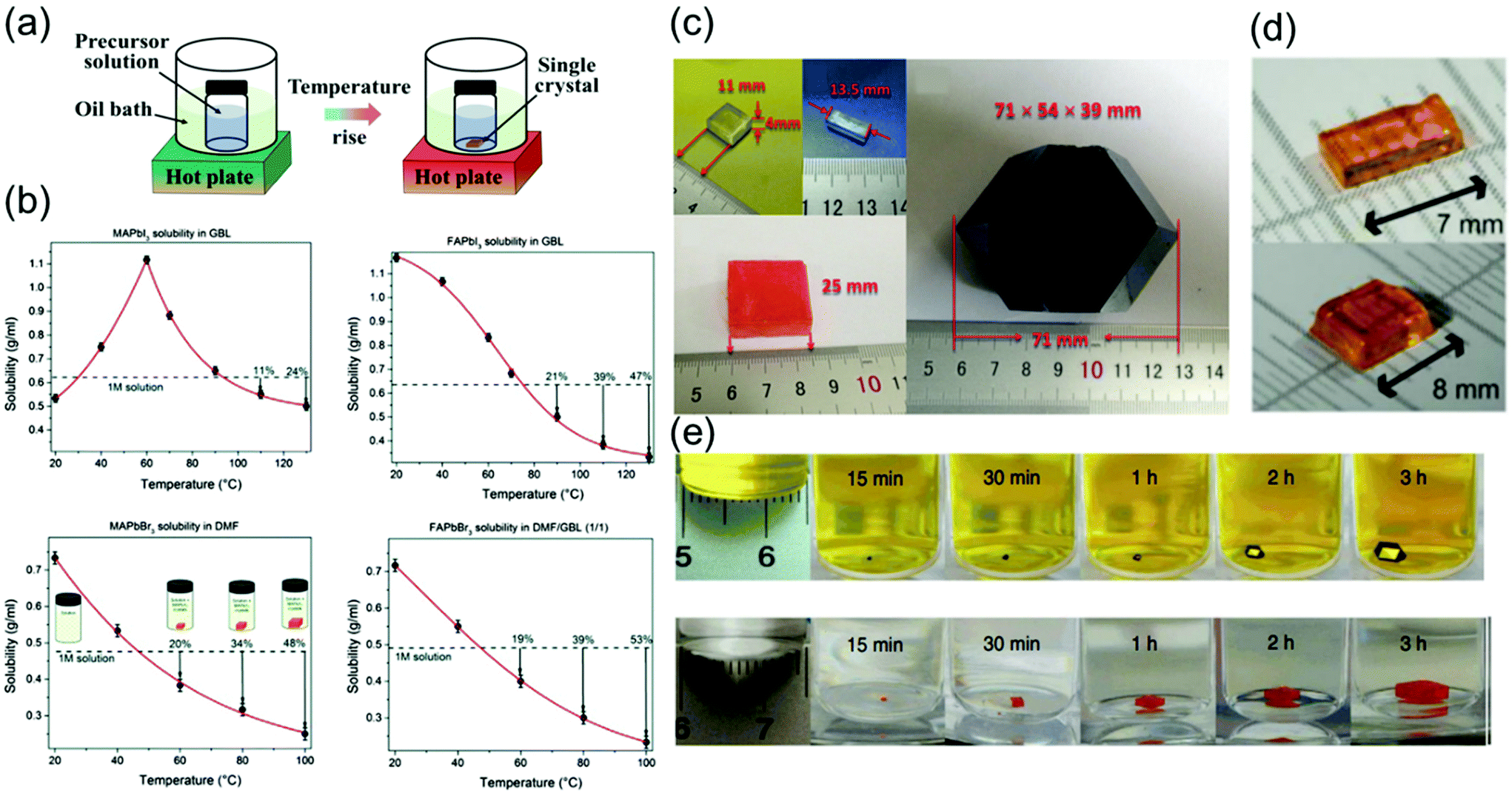 | ||
| Fig. 4 (a) Schematics of the ITC method. (b) Temperature-dependent solubility of MAPbI3 in GBL, FAPbI3 in GBL, and MAPbBr3 in DMF, showing yield at different temperatures, and FAPbBr3 in DMF:GBL (1:1, v/v). Reproduced with permission.63 Copyright 2015, RSC. (c) Images of the as-grown MAPbX3 crystals, X = Cl, Br, and I. Reproduced with permission.66 Copyright 2015, Wiley-VCH. (d) Photographs of the obtained CsPbBr3 single crystals. Reproduced with permission.30 Copyright 2016, ACS. (e) MAPbI3 and MAPbBr3 crystal growth at different time intervals. Reproduced with permission.22 Copyright 2015, Springer Nature. | ||
Saidaminov et al.63 grew single-crystal perovskites of MAPbX3 and FAPbX3 (where X = Br− and I−) using this method, as shown in Fig. 4b. The solubilities of these perovskites were assessed in different solvents at various temperatures to confirm their retrograde solubility behavior. DMF and GBL were found to be the appropriate solvents for promoting retrograde solubility in bromine and iodine-based perovskites, respectively. Fig. 4b shows the effect of temperature on the solubility of MAPbX3 and FAPbX3. The retrograde solubility behaviors of these perovskites in the aforementioned solvents are clearly confirmed by the obtained negative slopes.
As shown in Fig. 4c, in another study, large crystals of MAPbX3 (X = Cl, Br, and I) were obtained.66 The crystals of MAPbCl3 were transparent and cuboidal, and the MAPbBr3 crystals also had cuboidal shapes and orange color. However, the MAPbI3 crystals are commonly obtained as dodecahedrons and sometimes rhombohexagonal dodecahedrons.
As shown in Fig. 4d, Peng et al.30 showed that the orthorhombic-to-tetragonal phase transition, which reportedly occurs at 88 °C in thermodynamic equilibrium, is an important factor. Although a solubility gradient, such as the one shown in Fig. 1a, in principle allows the growth of single crystals, the particularly steep dependence for 1:2 CsBr:PbBr2 solutions in DMSO might also be a problem. Moreover, a faster oversaturation upon heating leads to the formation of multiple nuclei and/or polycrystals. These authors found that the solubility–temperature profile can be smoothened by the addition of cyclohexanol (CyOH) or a CyOH/DMF mixture. The single crystals grown using such solvent mixtures exhibited better reproducibility, and only 1–3 crystals per vessel were formed. These crystals nucleated at ∼90 °C and continued to grow up to a temperature of 110 °C without further nucleation.
The best quality single crystals were obtained at an overall growth rate of <0.2 mm h−1. Saidaminov et al.22 recorded the ITC-induced growth of MAPbI3 crystals on video in time-accelerated mode; several snapshots of the process are shown in Fig. 4e. Evidently, individual MAPbI3 crystals grew at a rate of ∼3 mm3 h−1 in the first hour. This rate significantly increased to ∼9 mm3 h−1 in the second hour and to ∼20 mm3 h−1 in the following hour. Notably, the observed growth rate of ∼20 mm3 h−1 is an order of magnitude greater than the previously reported highest growth rate.
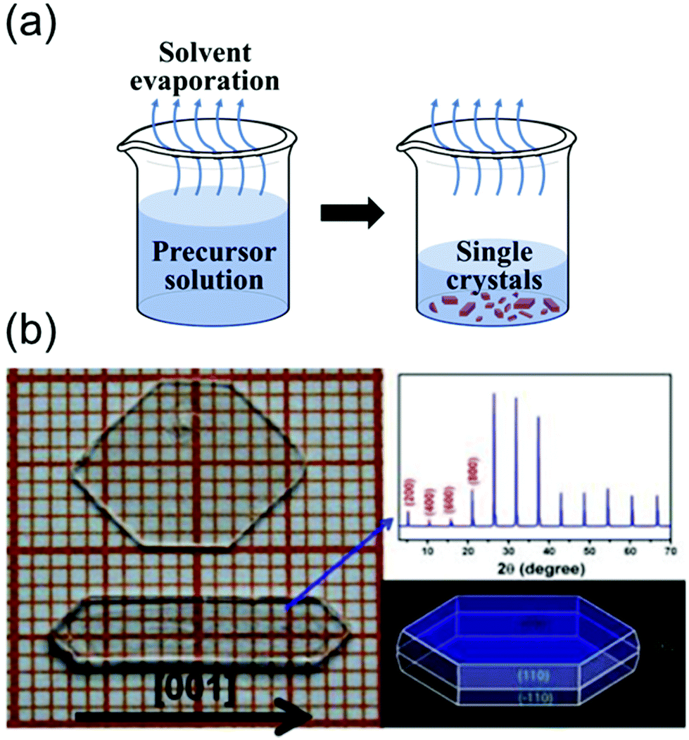 | ||
| Fig. 5 (a) Schematics of the solvent evaporation crystallization method. (b) Image of two large single crystals of BA2PbCl4, and the simulated morphology obtained using Material Studio. Photographs indicating the size of the MAPbCl3 single crystal as well as the (100) crystallographic plane. The single crystals were prepared at different temperatures. Reproduced with permission.69 Copyright 2015, Springer Nature. | ||
As shown in Fig. 5b, Liao et al.69 synthesized BA2PbX4 crystals (where BA is benzylammonium) and investigated their crystal structures and properties. They dissolved dichlorides of BA and Pb in a concentrated HCl solution in the stoichiometric molar ratio to form small crystals of BA2PbX4. However, a slowly evaporating DMF solution at 90 °C yielded transparent bulk crystals (size: 5 mm × 10 mm × 2 mm). Fig. 5(b) shows the photograph, X-ray diffraction (XRD) patterns, and morphology of the grown single-crystal perovskites. The XRD patterns indicated that the single crystal elongated along the [001] direction. These results indicate that the solvent evaporation method is extremely effective for growing pure single-crystal perovskites from solvents with low boiling points up to 100 °C.
:1 (0.2 M PbBr2), and MAI and PbI2 were dissolved in GBL at a molar ratio of 3:1 (0.5 M PbI2) as the precursors. First, a small bottle containing the precursors was placed into a larger container containing the antisolvent, and the entire vessel was then sealed. The DCM vapors slowly diffused into the solution as DCM mixes well both DMF and GBL, as shown in Fig. 6a. Because this method is not affected by temperature fluctuations, phase transition due to temperature changes does not occur, leading to the formation of crystals with a highly ordered lattice arrangement and smoother surfaces than those formed by the ITC method. In another reported study, inorganic CsPbBr3 single-crystal perovskites were formed using the antisolvent vapor-assisted crystallization method with additional titration of MeCN or MeOH as shown in Fig. 6b.70
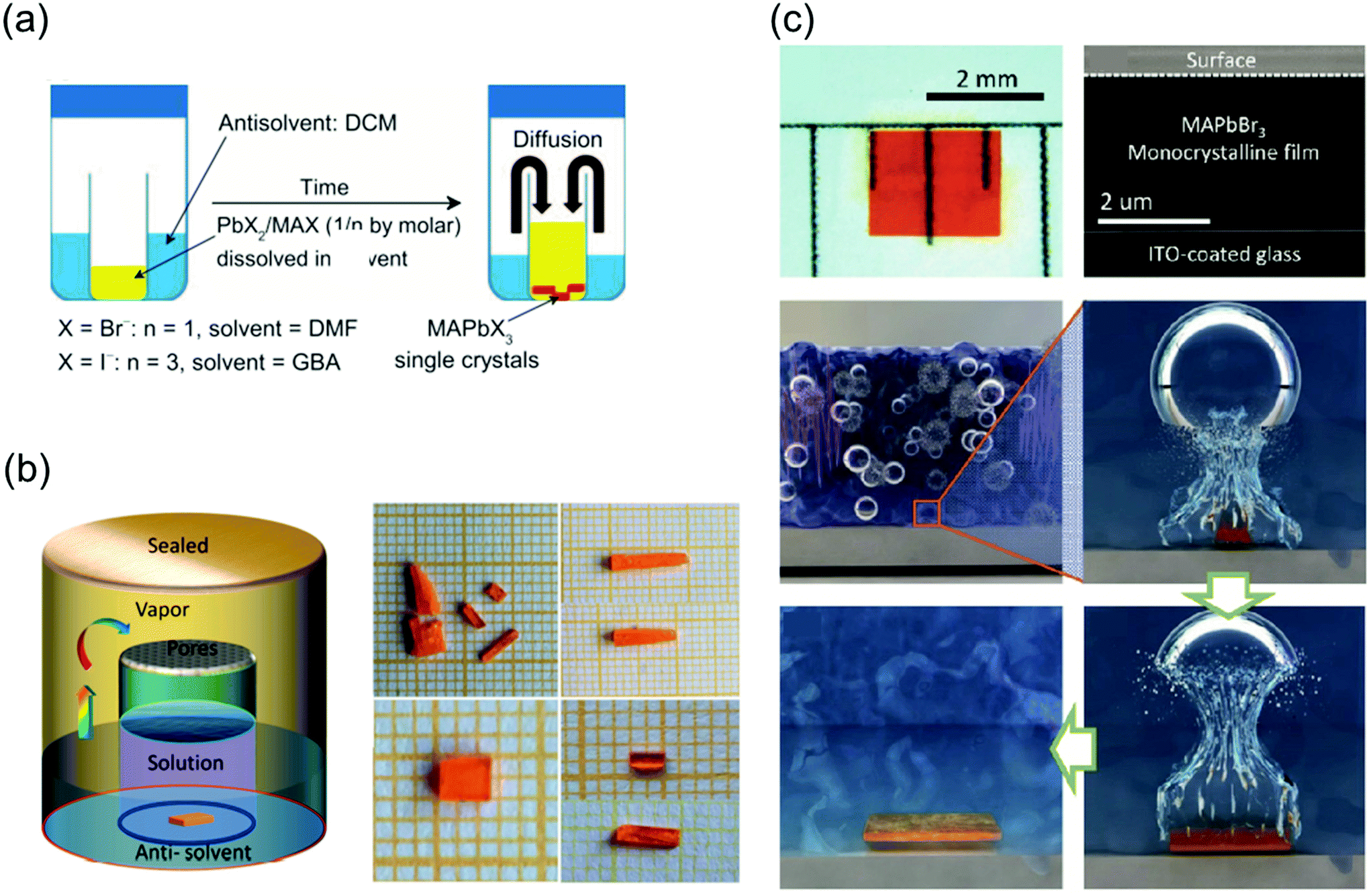 | ||
| Fig. 6 (a) Schematic diagram of the antisolvent vapor-assisted crystallization method. Reproduced with permission.28 Copyright 2015, AAAS. (b) Schematic representation of the single-crystal growth process via the antisolvent method, and photos showing the CsPbBr3 crystals grown at room temperature (polycrystalline, upper images) and 40 °C (single crystal, lower images), respectively. Reproduced with permission.70 Copyright 2017, ACS. (c) Cavitation-triggered asymmetrical crystallization method for directly growing micrometer-thickness single crystals on ITO substrates. Reproduced with permission.30 Copyright 2016, Wiley-VCH. | ||
One major limitation of the single crystals synthesized by the traditional ITC and antisolvent vapor-assisted crystallization methods is that it is difficult to deposit the single crystals onto substrates such as indium tin oxide (ITO) or fluorine-doped tin oxide (FTO) owing to the high nucleation energy barrier of smooth surfaces. Therefore, Peng et al.30 proposed a cavitation-triggered asymmetrical crystallization method, illustrated in Fig. 6c, which is essentially an improved antisolvent vapor-assisted crystallization. In this method, a 1 s long ultrasonic pulse, which plays an important role in the cavitation process, is introduced into the low-saturation precursor solution while the antisolvent vapors diffuse into it. The circulating sound waves constantly generate and collapse cavities. Thus, utilizing the transient high energy that is produced during the cavitation process to overcome the nucleation barrier, single crystals were directly grown on substrates such as silicon wafers, ITO-coated glass, FTO-coated glass, and silicon wafers coated with sputtered metals. By controlling the growth time and precursor concentration, the thickness of the resulting MAPbBr3 crystals can be adjusted from 1 to 50 μm. This method opens a new pathway to grow ultrathin perovskite single crystals directly on substrates, instead of evaporating electrodes on independent single crystals. Consequently, this method can be widely implemented to grow typical vertical structures on substrates for optoelectronic devices.
2.2. Advanced quality control
The recent advances in crystallization have contributed significantly toward enhancing our understanding of the crystallization mechanism and provided novel pathways to control the quality of single crystals grown via various crystallization techniques. Furthermore, the availability of diverse materials, tailoring of crystal shapes, and fast processing technology play key roles in the crystal growth. In this section, we focus on some of the key research trends in optimization control.To date, several perovskite single crystals have been synthesized through the polymer-controlled route. Fig. 7a shows images of the mixed-halide and mixed-organic cation perovskite single crystals (MAPbIxBr3−x, MAPbBrxCl3−x, MAyFA1−yPbBr3, and MAyFA1−yPbI3).79 The Br-based single crystals exhibit good transparency and have potential applications in optical devices. For such crystals, the growth process begins with perovskite powders, which are synthesized using a water bath method and are subsequently dissolved in organic solvents to obtain the precursor solutions, followed by a polymer-assisted growth of single crystals. Ng et al.80 successfully synthesized crystals, such as FAPbBr3−xClx-based perovskites, with total synthesis times of 20 h and >48 h and showed degradation of the surface with increasing synthesis time. Using DMF–GBL (1:1, v/v) as a solvent, perovskites of FAPb1−xSnxBr3 were successfully prepared by substituting an equal molar ratio of PbBr2 for SnBr2 under an inert atmosphere to prevent Sn oxidation.
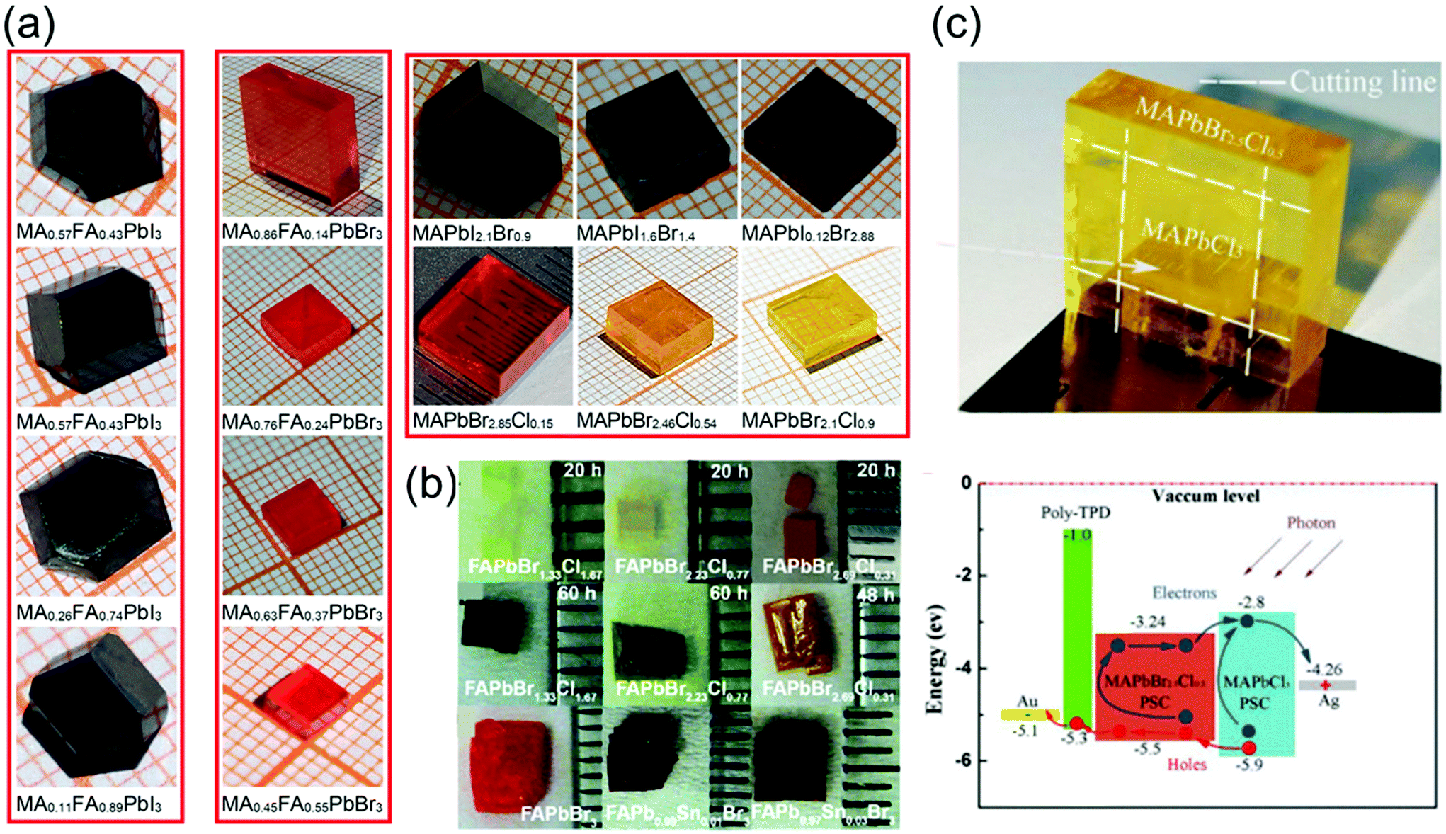 | ||
| Fig. 7 (a) Series of mixed-halide MAPbIxBr3−x and MAPbBrxCl3−x single crystals (0 ≤ x ≤ 3), and the mixed-organic cation MAyFA1−yPbX3 (X = I, Br) single crystals (0 ≤ y ≤ 1). Reproduced with permission.79 Copyright 2021, Springer Nature. (b) Photographs of the FAPbBr3−xClx-based perovskites (upper) with a total synthesis time of 20 h and (middle) >48 h, photographs of the FAPb1−xSnxBr3-based perovskites (lower). Reproduced with permission.80 Copyright 2020, RSC. (c) Optical image of the yellow-colored MAPbBr2.5Cl0.5 enfolding the transparent MAPbCl3 perovskite single crystals after epitaxial growth, and the energy level diagram of the PIN photodiode with epitaxial hole blocking layer (HBL). Reproduced with permission.81 Copyright 2020, Frontiers Media SA. | ||
Pan et al.81 used liquid-phase epitaxy to prepare MAPbCl3–MAPbBr2.5Cl0.5 heterojunction interfaces, in which the MAPbBr2.5Cl0.5 perovskite single crystal acts as the active layer, and the MAPbCl3 perovskite single crystal acts as the hole-blocking layer. Pristine MAPbCl3 perovskite single crystals, considered as n-type semiconductors, were grown using the temperature-changing crystallization methods, wherein the precursor solution was heated from 45 to 60 °C for 80 h. First, one unit of bulk MAPbCl3 perovskite single crystals was synthesized using the low-cost solution processes. Then, it was placed into the precursor solution of MAPbBr2.5Cl0.5 to induce the liquid-phase epitaxial growth, in which the solution was heated from 50 to 65 °C for 100 h. The MAPbBr2.5Cl0.5 perovskite single crystals slowly grew on the top and side of the MAPbCl3 crystals in the precursor solution. Finally, the heterojunction perovskite single crystals were extracted from the solution with MAPbBr2.5Cl0.5 enfolding the MAPbCl3 perovskite single crystals as shown in Fig. 7c. To fabricate a PIN photodiode, a p-type poly-temperature programmed decomposition (TPD)-produced thin film was deposited on the surface of the MAPbBr2.5Cl0.5 perovskite single crystals. Subsequently, Au and Ag thin films were deposited on the poly-TPD layer and the surface of the MAPbCl3 perovskite single crystals sequentially via thermal evaporation in a vacuum. The Au and Ag thin films act as the anode and cathode, respectively. The schematic energy level diagram of the fabricated PIN photodiode is shown in Fig. 7c.
The solution-assisted growth of perovskite single crystals results in complete dissolution without residual molecules and allows control of the growth temperature, which is necessary for determining the quality of the synthesized single crystals. Fig. 8a shows the inverse solubility of the MAPbBr3 precursor in DMF solvent. As mentioned before, the MAPbBr3 single crystals can be formed using the ITC method because of inverse solubility, which is demonstrated by the experimental values of solubility in the temperature range from 100 to 20 °C (gray curve) in Fig. 8a.63 As an advanced ITC technique, Cho et al.82 performed low-temperature dissolution below 0 °C based on the measurement of low-temperature inverse solubility for the first time, as shown in Fig. 8a. They evaluated each single crystal, with different dissolution temperatures of 20, 0, and −40 °C, kept in different baths under air, ice, and dry ice, and found that the resulting MAPbBr3 single crystals that dissolved at −40 °C showed the largest sizes and the best electrical properties. The results were explained using the MAPbBr3–DMF complex, which completely dissolved at low temperatures. Notably, the long time required to dissolve the precursor was shortened through the low-temperature dissolution process. Fig. 8a also illustrates the heating rate of crystallization in three different regions as well as the growing process at each temperature. By controlling the heating rate, both the quality and size of the crystals could be controlled, resulting in the formation of large-sized high-quality single crystals within only 6 h. Initially, the heating rate was 0.5 °C min−1 between 20 and 60 °C, gradually decreasing to 0.33 °C min−1 between 60 and 100 °C, and finally decreased to 0.25 °C min−1 at temperatures >100 °C. The increase in the crystal size was prominently due to the increase in the temperature. In addition, although the heating temperature was controlled from 20 to 110 °C according to the three different dissolution conditions, the temperature at which the seed crystal formed was different (indicated by the point and arrow in the figure). At the lower dissolution temperature, the single-crystal seed formed at a lower temperature, which was the starting point of the single-crystal growth.
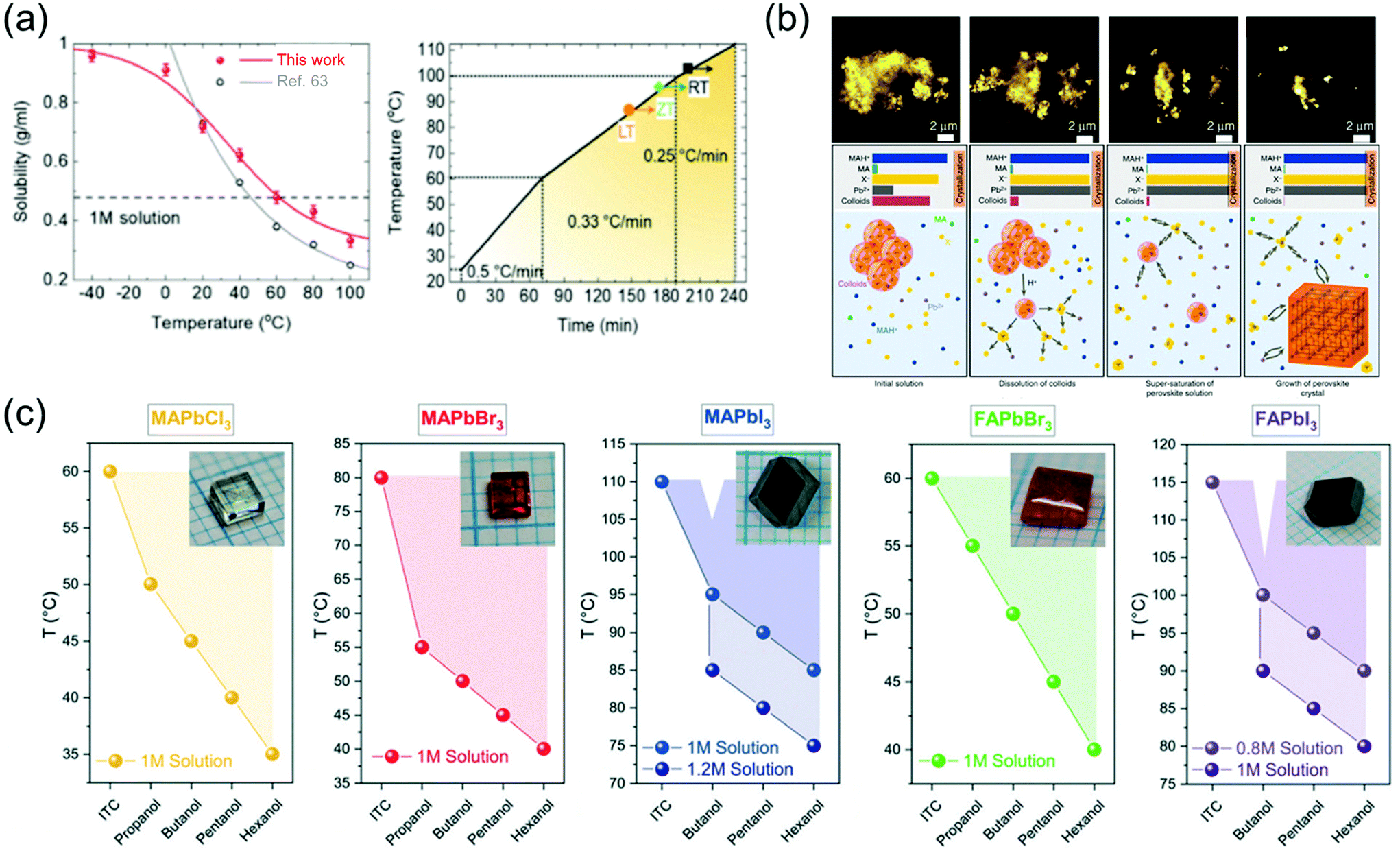 | ||
| Fig. 8 (a) Temperature-dependent solubility of MAPbBr3 in DMF compared with that reported in ref. 63 and the heating rate of crystallization for a high-speed process. Reproduced with permission.82 Copyright 2021, RSC. (b) Schematic representation of the crystallization mechanism, including the formation process. Reproduced with permission.85 Copyright 2020, Wiley-VCH. (c) Dependence of the OLTP crystallization temperatures on the applied alcohols, and the molar concentrations of the solutions used for growing crystals in 3–5 h. Reproduced with permission.84 Copyright 2021, RSC. | ||
Nayak et al.83 presented compelling evidence that the observed rapid crystallization of metal halide perovskite crystals results from the dissolution of colloids, which occurs because of a change in the solvent strength and acidity of the solution. The dissolved colloids increase the concentration of free ions in the solution, leading to supersaturation and the onset of crystallization. They added formic acid (FAH) to DMF and γ-hydroxybutyric acid to GBL, and reportedly, the crystallization began within 5 min. Interferometric scattering microscopy results showed a time sequence of the iodide salts dissolving in GBL after the addition of FAH, and the mechanism of crystallization is summarized in Fig. 8b. The schematic shows several key points of the inverse temperature growth mechanism, including the initial solution, dissolution of colloids, supersaturation of the perovskite solution, and growth of the perovskite crystal. In the initial state of the solution, most of the Pb2+ and halide ions were contained in the colloids, resulting in the depletion of all the components added to the solution. The following cases occur when the temperature is increased: first, the colloid decomposes and releases a large amount of Pb2+ and halide ions, inducing crystallization due to the increase in the solution concentration; second, protonation of MA increases the concentration of MAH+ in the solution; third, the role of the solvent becomes weaker because of the lower concentration of MA. Therefore, perovskite single crystals rapidly grow because of the acid-induced dissolution of colloids.
To grow large-sized perovskite single crystals in the shortest possible time with the lowest possible energy consumption, Höcker et al.84 developed a crystallization process—a combination of reactive crystallization and ITC, namely RITC—based on primary alcohols, which significantly affect the growth temperature of the crystals and reduce the solubility. In addition, the less polar hexanol allows crystal growth at lower temperatures than does the polar propanol. Fig. 8c shows the RITC single crystals successfully grown using the reagent hexanol. In contrast to ITC, the admixture of additives used in RITC enables crystal pulling at lower temperatures, as shown in Fig. 8c. The colored dots in the figure represent the lowest possible growth temperature when the respective alcohol is added. For RITC, approximately 100 μl of one of the primary alcohols was added to each precursor solution at room temperature. The growth temperatures were reduced by up to 40 °C using the reagent hexanol for the above-mentioned molar concentrations; for TMAPbCl3, TMAPbBr3, TMAPbI3, TFAPbBr3, and TFAPbI3, the growth temperatures were 35, 40, 85, 40, and 90 °C, respectively. Although the MAPbCl3, MAPbBr3, and FAPbBr3 precursor solutions were already saturated, the molar concentration was further increased for the iodine-containing solutions. In this case, MAPbI3 (c = 1.2 mol l−1) and FAPbI3 (c = 1 mol l−1) crystals started to grow even at 75 and 80 °C, respectively, which represent a temperature difference of 35 °C with respect to that observed in ITC. Due to the colder growth conditions, the precursor solutions could also be used for growth periods longer than 5 h to grow large-sized perovskite crystals. Another benefit of RITC is that the organo-Pb trihalide perovskite (OLTP) crystal growth is no longer limited to one temperature value. The colored areas in Fig. 8c illustrate the crystal growth range from the lowest temperatures used in RITC up to the temperatures used in ITC. For MAPbBr3, the largest growth ranges from 40 to 80 °C was observed.
To grow a single-crystal perovskite MAPbI3 wafer, Liu et al.86 employed an ultrathin geometry-defined dynamic-flow reaction system, which was placed in a flat container with two thin glass slides separated by two spacers with predefined separation to confine the crystal growth within the slit channel. The geometry is illustrated in Fig. 9a. They reported a thinness- and shape-controlled growth method to grow perovskite single crystals. With a pump to supply fresh solution, the thickness of the perovskite single crystals was controlled by changing the thickness of the spacers from 150 to 1440 μm as shown in Fig. 9a. As depicted in Fig. 9b, two clean and flat substrates were clipped together and then immersed vertically in the perovskite precursor solution, and the capillary pressure forced the solution onto the entire substrate surface. The thickness of the solution-coated film depended on the distance between the substrates, which was easily tuned from nano- to micrometers by changing the clipping force. To control the solvent evaporation rate, the bottom precursor solution was heated. Following TSSG,5 the bottom solution maintained at the saturation state, whereas the top solution film was supersaturated because of the cooler conditions, leading to the crystallization of the perovskite in the clipped solution film. Simultaneously, a temperature gradient caused sufficient convection from the bottom to the top, supplying material for the continuous growth of the perovskite single crystals. After a certain time, perovskite single-crystal thin films formed in the space confined between the clipped substrates. The thickness of the single-crystal thin films was well defined by the distance between the two substrates, which could be easily tuned by the clipping force. To control and scale the production process of the perovskite single-crystal films, Gu et al.49 fabricated perovskite seeds on a substrate using the inkjet printing method, which is a facile technology used to perform selective deposition of functional materials and their patterns, as shown in Fig. 9c. Accordingly, perovskite solution droplets were selectively deposited onto a substrate. As the droplets evaporated, patterned perovskite seeds, namely, the perovskite seed stamp, formed on the substrate, which was then covered with the saturated perovskite solution. By drying the solvent at room temperature, single-crystal films were grown uniformly and in situ on the seeds across the whole substrate. The covered stamp was then peeled off to print the perovskite single-crystal films directly on the substrate. The seeds exhibited a dominant effect on the single-crystal film formation, because they effectively inhibited random nucleation and triggered the growth of single-crystal films. Using this method, controlled preparation of millimeter-sized perovskite single-crystal films was performed in batches. Rao et al.89 reported a limited space filled with the flowing precursor solution containing 1.1 M PbBr2 and MABr dissolved in DMF to obtain thickness-controllable laminar MAPbBr3 single crystals. Fig. 9d shows photographs of the laminar MAPbBr3 single crystals deposited on TiO2-coated FTO glasses (size: 6 mm × 8 mm). Two FTO glasses were used as the growth substrates, in which a sandwiched polytetrafluoroethylene (PTFE) bounding box was added to construct the growth space. For the in situ growth of MAPbBr3 single crystals, FTO glass, TiO2-coated FTO glass, ITO glass, or other rigid plates can be used as the substrates. Furthermore, to decide the thickness of the laminar single crystals, the thickness of the PTFE thin membrane (such as 20, 35, and 50 μm) was controlled. The substrate was locally heated to a temperature of 90 °C, and the MAPbBr3 single crystals primarily grew on the hot region, as laminar crystals because of space limitation, via ITC of MAPbBr3 in DMF. Two holes were drilled into each substrate, and a peristaltic pump was employed to ensure that the precursor solution kept flowing, sustaining the growth of the single crystals for two days.
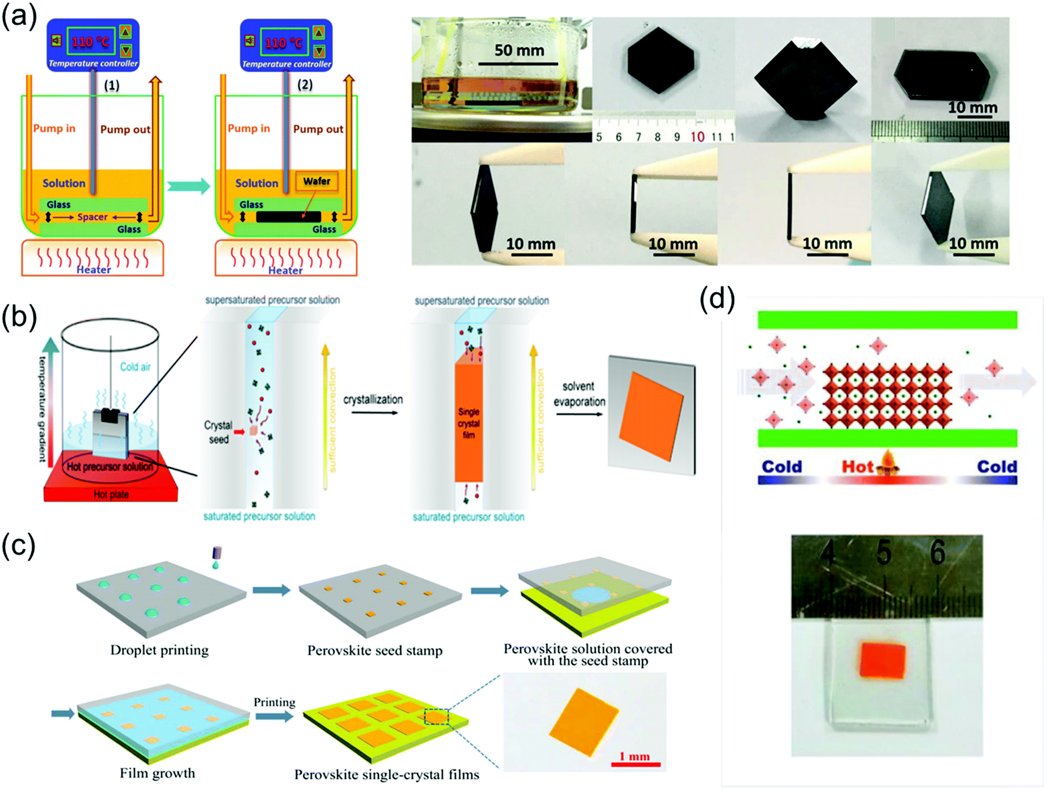 | ||
| Fig. 9 (a) Schematic illustration of the ultrathin MAPbI3 single-crystal wafer preparation and photograph of the single-crystal wafer growing in the microreactor system with different thicknesses and shapes. Reproduced with permission.86 Copyright 2016, Wiley-VCH. (b) Schematic illustration of a spatially confined solution-processed strategy for on-substrate growth of various hybrid perovskite single-crystal thin films. Reproduced with permission.87 Copyright 2016, RSC. (c) Schematic illustration of the scalable growth of single-crystal perovskite thin-film arrays prepared using the inkjet printing method. Reproduced with permission.88 Copyright 2018, AAAS. (d) Photograph of an MAPbBr3 laminar single crystal grown on FTO glass. Reproduced with permission.89 Copyright 2017, RSC. | ||
3. Characterization techniques for optoelectronic properties
Perovskite single crystals have garnered significant attention because of their superior optoelectronic properties compared with their polycrystalline counterparts. The intrinsic properties of perovskite single crystals also enable in-depth study of physical and chemical properties. Because the characterization of perovskite single crystals is essential to realize their high-performance application in various fields, it is necessary to master the relevant characterization techniques to investigate their optoelectronic properties.3.1. Optical absorption and luminescence properties
In optoelectronic devices, the bandgap of the semiconductor material determines its light absorption wavelength. Shi et al.28 synthesized MAPbX3 (X = Br− or I−) single crystals using the antisolvent vapor-assisted crystallization method and investigated their absorbance as depicted in Fig. 10a, which shows a clear band-edge cutoff with no excitonic signature, suggesting a minimal number of in-gap defect states. By extrapolating the linear region of the absorption edge to the energy-axis intercept, Shi et al. determined the optical bandgaps of MAPbBr3 and MAPbI3 single crystals to be 2.21 and 1.51 eV, respectively. Both the materials in their single-crystalline form exhibit a substantially narrower bandgap than do the corresponding films. Such a narrow bandgap can enhance photon harvesting and hence improve the photocurrent generation. Both MAPbBr3 and MAPbI3 exhibit a narrow photoluminescence (PL) peak near the band edge. A noticeable shoulder at ∼790 nm observed in the PL spectrum of MAPbI3 single crystals agrees with that of the thin films,8 in which the main PL peak, located at 820 nm, can be attributed to the intrinsic PL emission from the MAPbI3 crystal lattice.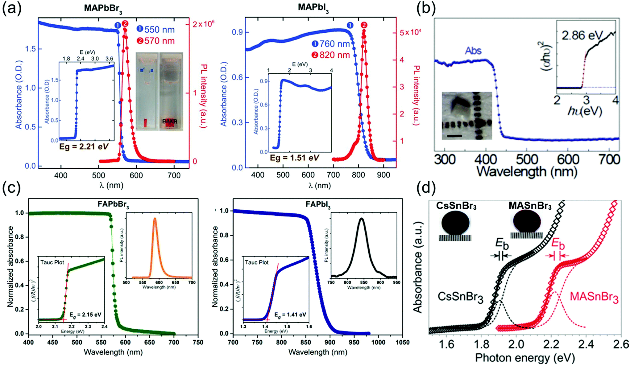 | ||
| Fig. 10 (a) Absorbance and PL spectra of MAPbBr3 and MAPbI3 single crystals. Insets: Absorbance versus photon energy and the determined bandgap (Eg). Reproduced with permission.28 Copyright 2015, AAAS. (b) Optical absorption of CsPbCl3 with a tetragonal perovskite structure. Inset: (αhν)2 ∼ hν Tauc plot. Inset: Optical microscopy curve of the CsPbCl3 single crystal showing the enlarged (002) and (200) peaks. Reproduced with permission.21 Copyright 2020, Optica Publishing Group. (c) Steady-state absorption of FAPbBr3 (left) and FAPbI3 (right) single crystals. PL spectra (right insets) and Tauc plots (left insets). Reproduced with permission.3 Copyright 2016, ACS. (d) Experimental and fitted absorption edges of CsSnBr3 (black) and MASnBr3 (red). The gap between the exciton peak and the band edge equals the exciton binding energy (Eb). Photograph of a CsSnBr3 disk (left), and an MASnBr3 disk (right) next to a millimeter ruler. Reproduced with permission.20 Copyright 2018, Wiley-VCH. | ||
Rao et al.21 reported the optical absorption spectrum of CsPbCl3 single crystals as shown in Fig. 10b. The absorption edge is located at 430 nm, and the direct optical bandgap was calculated to be 2.86 ± 0.3 eV by linear fitting of the (αhν)2 ∼ hν Tauc plot. The bandgap of CsPbCl3 agrees well with the reported value of 2.86 eV determined by density functional theory calculations and UV-Vis-IR absorption spectroscopy.92 The bandgap of tetragonal CsPbCl3 is lower than that of cubic CsPbCl3, with a reported value of 2.92 eV for polycrystals and ∼2.98 eV for microwire networks.93
Next, Zhumekenov et al.3 studied the optical properties of synthesized FAPbX3 (X = Br− and I−) crystals as shown in Fig. 10c. The absorption spectra were obtained by converting the reflectance data using the Kubelka–Munk equation:94f(R) = (1 − R)2/(2R), where R is the radius. Contrary to the perovskite polycrystalline films,95,96 the absorption profiles of the FAPbX3 single crystals appear flat with a clear band-edge cutoff with no excitonic signature, suggesting a minimal density of in-gap defect states. The optical bandgaps estimated from the corresponding Tauc plots are 2.15 and 1.41 eV for the FAPbBr3 and FAPbI3 crystals, respectively, which are in good agreement with those reported in other studies.63 The PL peaks of the FAPbBr3 and FAPbI3 single crystals are located at 587 and 843 nm, respectively. Notably, the PL peak of the FAPbX3 single crystals (located at 550 nm for FAPbBr3 and at approximately 810 nm for FAPbI3) is remarkably red-shifted compared with that of the polycrystalline films.97,98 This observed spectral shift is consistent with that reported in previous studies22,28,39 and is attributed to the highly ordered structure and low-density defects in the single crystals.8,28
Fig. 10d depicts the absorption spectra of the transparent submicron-thick films of CsSnBr3 and MASnBr3.20 Both the spectra consist of a steeply rising absorption edge, which turns to a gentle slope, obtained via high-energy absorption crystallography and absorption spectroscopy of both the tin-based perovskites, performed to identify their lattice parameters (a) and bandgap energies (Eg), respectively. Based on the experimental cell dimension, the Eg of CsSnBr3 was calculated using the quasiparticle self-consistent GW method (G is the Green's function, W is the screened Coulomb interaction),99 which is an elaborated theory appropriate for calculating the electronic band structure of semiconductors. Complexity in the structural representation of MASnBr3 was avoided by replacing its disordered MA+ with a static Cs+ while fixing the lattice parameter. An excellent agreement between the experimental and calculated Eg values of both CsSnBr3 and MASnBr3 established the validity of the computational method and model.
3.2. Carrier transport
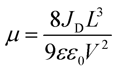
The charge-carrier transport in perovskite single crystals is generally revealed by the trap density, mobility, diffusion length, and lifetime. For developing optoelectronic devices, it is crucial to understand the effect of defects and carrier transport mechanism. The basic optoelectronic parameters of perovskite single crystals are summarized in this section.Liu et al.100 obtained the trap-state density (ntrap) in FAPbI3 from the dark current–voltage (I–V) curves for a hole-only device with the Au/FAPbI3/Au structure. The dark I–V curve exhibits three regions, as shown in Fig. 11a. When the applied voltage is lower than the kink-point voltage, the current increases linearly with the applied voltage, demonstrating an ohmic response between the Au electrode and the perovskite in the hole-only device. From this region (n = 1), the conductivities (σ) of FAPbI3 are estimated to be 1.8 × 10⁻⁸ Ω−1 cm−1. As the applied voltage exceeds the first kink-point voltage, the current exhibits a quick non-linear increase (n > 3), indicating that all the trap states are filled by the injected carriers. The applied voltage at the kink point is defined as the trap-filled limit voltage (VTFL), which is determined by the trap-state density as:101
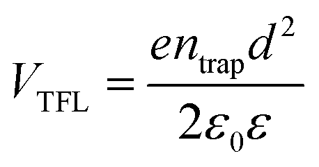 | (1) |
 | (2) |
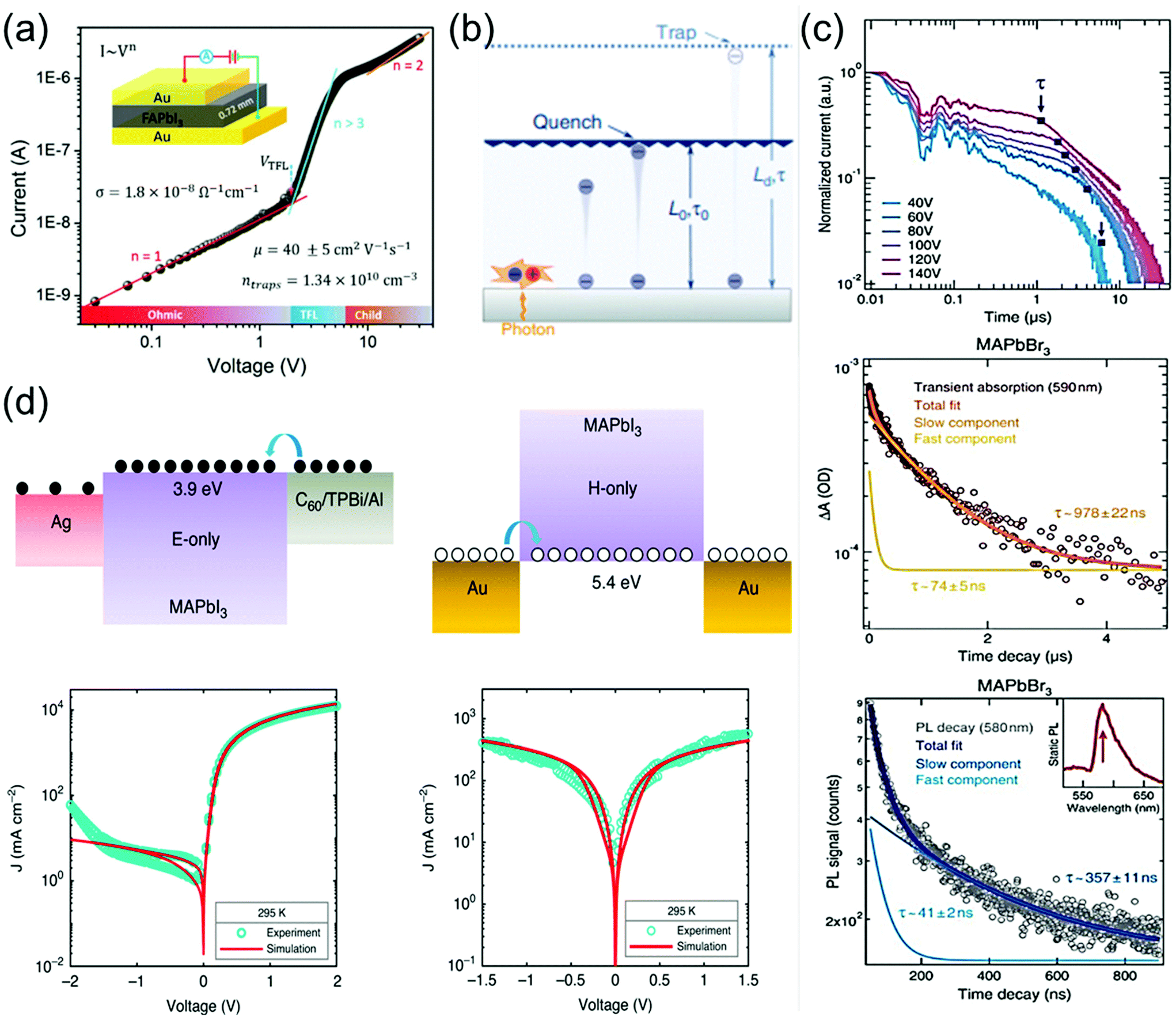 | ||
| Fig. 11 (a) Dark I–V response of a perovskite wafer exhibiting different regions, obtained from the log(I) versus log(V) plot. Reproduced with permission.100 Copyright 2016, Wiley-VCH. (b) Concept of diffusion-quenching models. A one-dimensional diffusion-quenching structure; carrier tunnelling process occurring at the interface between the active material and the carrier extraction layer. Reproduced with permission.108 Copyright 2019, Springer Nature. (c) Time-of-flight traces showing the transient current after photoexcitation at time t = 0 in a bi-logarithmic plot; the transit time t is identified at the corner of each trace and marked by blue squares. Transient absorption in MAPbBr3 crystals, evaluated at 590 nm, showing a fast component together with a slower decay. PL time decay trace of an MAPbBr3 crystal at 580 nm, with bi-exponential fits showing a fast and a slow transient. (d) Electron-only device, using a C60 (5 nm)/TPBi (5 nm)/Al electron-injection layer structure (left), schematic of the hole-only device, using bottom and top electrodes of Au (right). Reproduced with permission.107 Copyright 2020, Springer Nature. | ||
3.3. Defect analysis
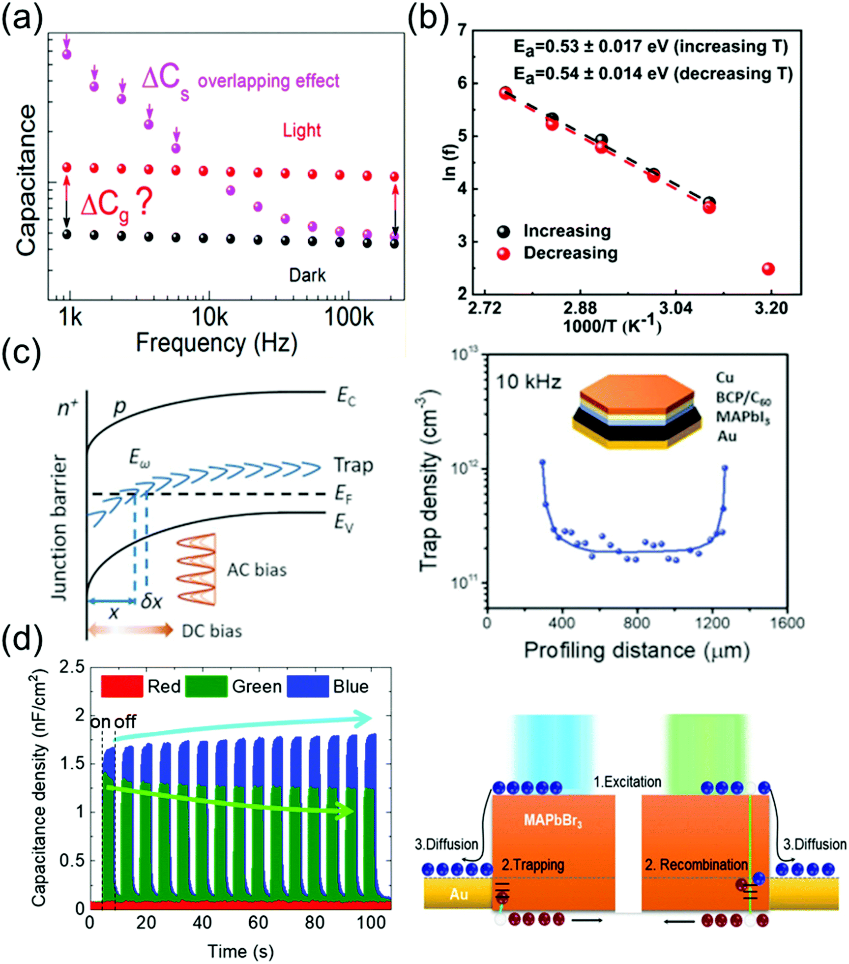
Ion migration, which is an intrinsic property of ionic perovskite materials, occurs in polycrystalline perovskite single crystals.109 However, the effects of defects in perovskite materials are unavoidable at the surface and grain boundaries, even though the single-crystal structure contains fewer grain boundaries and thus the ion migration channel can be eliminated. Thus, the influence of defects in perovskite single crystals should be investigated to prevent carrier recombination that causes electrical loss. Moreover, defects also cause instabilities in the crystals, including device degradation or hysteresis under ambient conditions and high temperatures. Defect analysis, including the distribution of trap states110–112 and activation energy of the defects,113 has been conducted not only for polycrystalline thin films114,115 but also for single-crystal structures. Moreover, to control the carrier concentration and mobility in devices, an in-depth knowledge of the carrier transport mechanism is essential.Almora et al.111 reported light-induced defects or dielectric changes in MAPbI3 perovskite single crystals. In Fig. 12a, the capacitance–frequency (C–F) curve shows the overlapping effect, resulting from the accumulated capacitance, under illumination. The overlapping can be broad and reveals the evolution of capacitance spectra with the irradiated light intensities. Evidently, no light-induced change in the dielectric properties of the perovskite material can be derived from these measurements. Therefore, the masking effect created by the overlapping between the accumulated capacitance (Cs) and the geometrical/chemical value was measured. The capacitance–voltage analysis at a given frequency that directly yields the capacitance value is influenced by the Cs overlapping effect. However, any light-induced dielectric change in the bulk cannot be inferred from these measurements.
 | ||
| Fig. 12 (a) C–F curve of an MAPbI3 single-crystal device under dark conditions and under illumination. Reproduced with permission.111 Copyright 2018, ACS. (b) Arrhenius plots of the inflection frequencies vs. 1000/T (ln(f0) vs. 1000/T) with the increasing and decreasing temperature of the MAPbI3 single crystal. Eact is the activation energy for the traps. Reproduced with permission.113 Copyright 2020, ACS. (c) DLCP technique. (left) Schematic of band bending of a p-type semiconductor with deep trap states in an n+–p junction. (right) The inset shows the device structure. Reproduced with permission.110 Copyright 2020, AAAS. (d) Time-dependent photocapacitance under red, green, and blue light illumination, and schematic of the carrier transport mechanism for MAPbBr3 under blue and green light illumination. Reproduced with permission.112 Copyright 2021, IOP Publishing. | ||
Kalam et al.113 presented the frequency-dependent capacitance plots at different temperatures. No significant difference was observed between the C–F curves obtained during the increasing and decreasing temperature cycles. As expected, the capacitance in the low-frequency region increases with the increasing temperature. From the obtained C–F plot, a change in the inflection frequencies (f0) in the range of 101–102 Hz was observed. Fig. 12b shows the plots of ln(f0) vs. inverse of temperature. From the slope of these curves, the activation energies were obtained as 0.53 ± 0.17 and 0.54 ± 0.14 eV during the heating and cooling of the MAPbI3 crystals, respectively. This small difference in the activation energy value was possibly due to the local lattice distortion during the tetragonal–cubic phase transition of the MAPbI3 single crystals. Reportedly, point defects due to ion migration are generated in MAPbI3 when the activation energy is in the range of 0.1–0.6 eV, which depends on the applied characterization method and material crystallinity. The obtained activation energy corresponds to ion migration, which further confirms our results that the associated capacitance in the low-frequency range (<103 Hz) originates from the mobile ions.
Ni et al.110 applied the deep-level capacitance profiling (DLCP) method to examine the spatial distribution of defects in the bandgap of perovskite single crystals. The DLCP method determines the carrier concentration with junction capacitance, including the free-carrier and trap concentration. If the spatial property of the semiconductor does not change drastically, then the differences in the profiling distance closely approximate the actual changes in the position, where the trap states influenced the capacitance, thus reflecting the change in the trap density in real space. In principle, high-resolution DLCP can be performed, because the depletion edge can be continuously tuned by the applied DC bias as shown in Fig. 12c. However, the profiling distances within the real devices are affected by the non-planar depletion interfaces caused by the surface roughness or heterogeneity of the materials, which can compromise the resolution of the profiling distance. Fig. 12c shows the DLCP measurements of an MAPbI3 single-crystal device with the Au/MAPbI3/C60/bathocuproine (BCP)/Cu structure, demonstrating the DLCP-assisted spatial profiling of trap densities in MAPbI3 single crystals. The trap density near the interface region was ∼10-fold greater than that inside the MAPbI3 single crystal. This difference indicates that the dangling bonds at the surface of the crystal form charge traps.
Cho et al.112 examined the photoresponse of MAPbBr3 single crystals, including the time-dependent photocapacitance of the single-crystal device under three incident light wavelengths (red, green, and blue light). The photocapacitance decreased with time under the green light, whereas under the blue light, the capacitance increased. In contrast, the device capacitance showed no photoresponse under the red light. The increase (overshooting) or decrease (saturation) of the photocapacitance in MAPbBr3 single crystals was analyzed based on the recombination and trapping of carriers at the defect states, respectively, as shown in Fig. 12d. According to these authors, the slow exponential decay of photocapacitance can be interpreted as the release of accumulated carriers in the defect states and reorientation of ion migration.
3.4. Surface properties
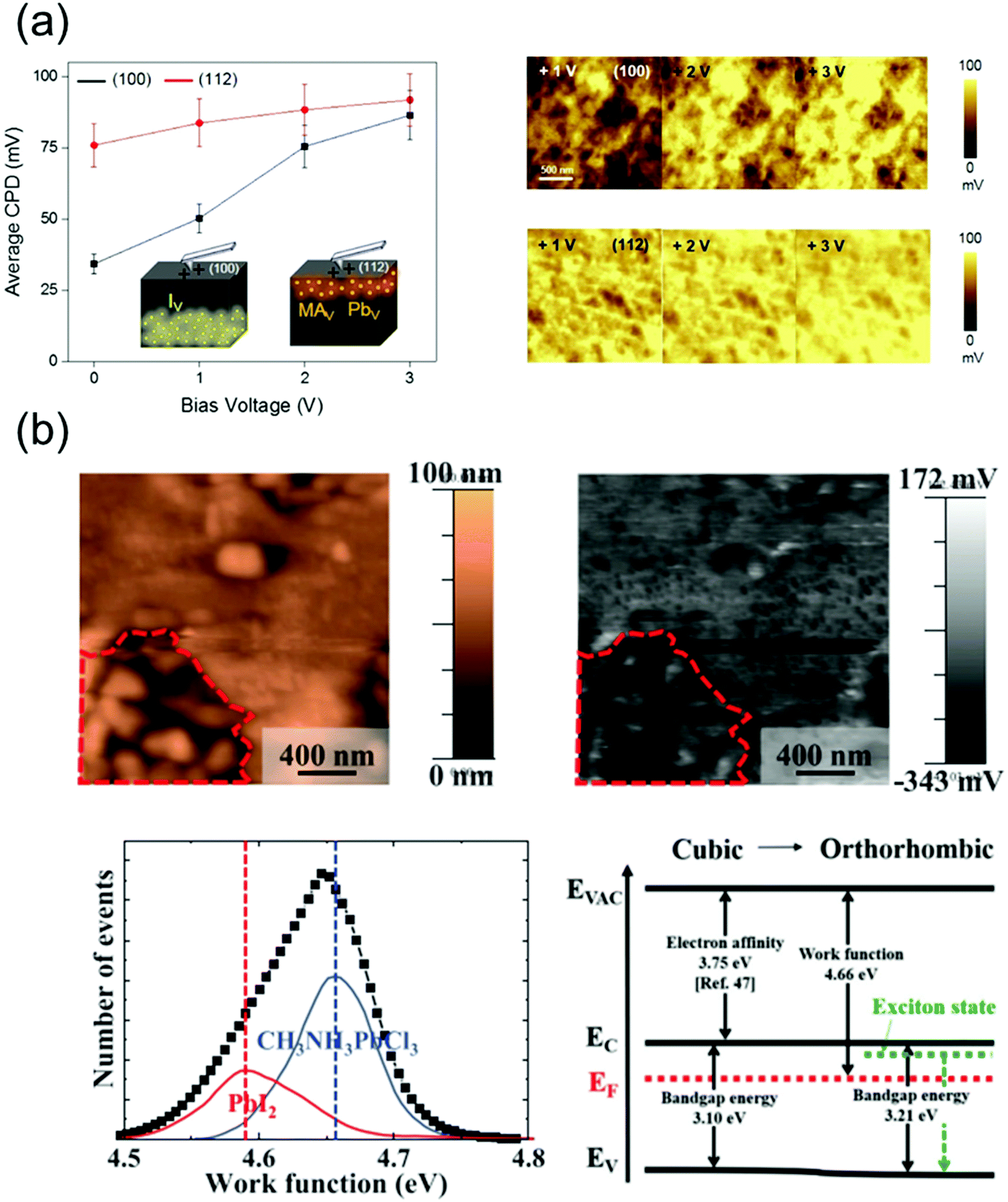
The ion migration, caused by the ionic defects in perovskite materials, influences their bandgap and absorption properties, thus affecting the operational state of the devices fabricated using these materials. This results in a photo- or field-induced dielectric constant and phase separation in the perovskites. It has been reported that the I− and MA+ ions, which theoretically exhibit low activation energies,116 act as possible channels for ion migration on the surface and grain boundaries of the perovskites.109 Although the perovskite single crystals exhibit a higher defect tolerance, they contain ionic defects, which are essentially absent in polycrystalline perovskites.117 Therefore, the surface properties of perovskite single crystals should be analyzed in detail as well.Kim et al.118 observed the different ion migration phenomena on the (100) and (112) facets of MAPbI3 single crystals using the Kelvin probe force microscopy (KPFM) technique, which is used to analyze the local surface potential differences induced by a specific ionic charge state. Fig. 13a shows the variations in the average contact potential difference (CPD), extracted from the KPFM images of the (100) and (112) oriented crystal surfaces under dark conditions, as a function of the positive and negative biases. When the positive biases were applied, the average CPD relatively increased on the (100) facet, whereas a moderate CPD increase was indicated on the (112) facet. According to the results, it was likely that among all the possible migrating ions (MA+, Pb2+ and I−), the positively charged iodide vacancy moved away from the surface under the applied positive bias. The n-type behavior of the surface deteriorated, which is consistent with the observed CPD increase. In contrast, the variation of CPD on the (112) facet under the applied positive voltage showed a relatively small change, which implies that the surface preserved the p-type properties under this condition. Based on these results, the authors suggested that the (112) facet predominantly contained difficult-to-move MA+ and Pb2+ defects with large activation energies. Thus, through this reported study, the authors demonstrated ionic movement on different facets of the MAPbI3 single crystals.
 | ||
| Fig. 13 (a) Ion movement on different facets of MAPbI3 single crystals, investigated by KPFM. Average CPD on the (100) and (112) facets as a function of the negative bias voltages (left), series of KPFM images of each facet after applying a positive bias (right). Reproduced with permission.118 Copyright 2019, ACS. (b) Topography and surface potential of the MAPbCl3 crystal (upper), the distribution of deconvoluted work function and band structures with cubic and orthorhombic phases (lower). Reproduced with permission.119 Copyright 2021, AIP Publishing. | ||
Jung et al.119 grew an MAPbCl3 single crystal with a well-defined structure and revealed the free and bound excitonic behaviors depending on the structural phase transition. Fig. 13b shows the topography and surface potential of the MAPbCl3 crystal obtained using KPFM. The work function can be calculated from these results. Although most of the surfaces in the MAPbCl3 single crystal were uniform, the observed uneven surface morphology (indicated by the region around the red dot) indicated a local phase separation. The most uniform surfaces of MAPbCl3 exhibited a work function of 4.66 eV, and the corresponding peak was deconvoluted at 4.58 eV owing to the decomposed PbI2. The phase separation due to local decomposition was explained by the deconvolution of the work function peaks such as those of MAX+ or PbX2+ (X = halide ion).120 Therefore, the deconvoluted work function peak of MAPbCl3 can reveal defects as MACl or PbCl2, which are generated because of decomposition. Based on the KPFM results, the band diagram was constructed, which indicated n-type characteristics. The observed work functions resulted from Pb segregation, which acted as n-type doping on the perovskite surface. Thus, the disordered phase and defects at the surface of the perovskite single crystals were investigated using the work function distribution.
4. Stability
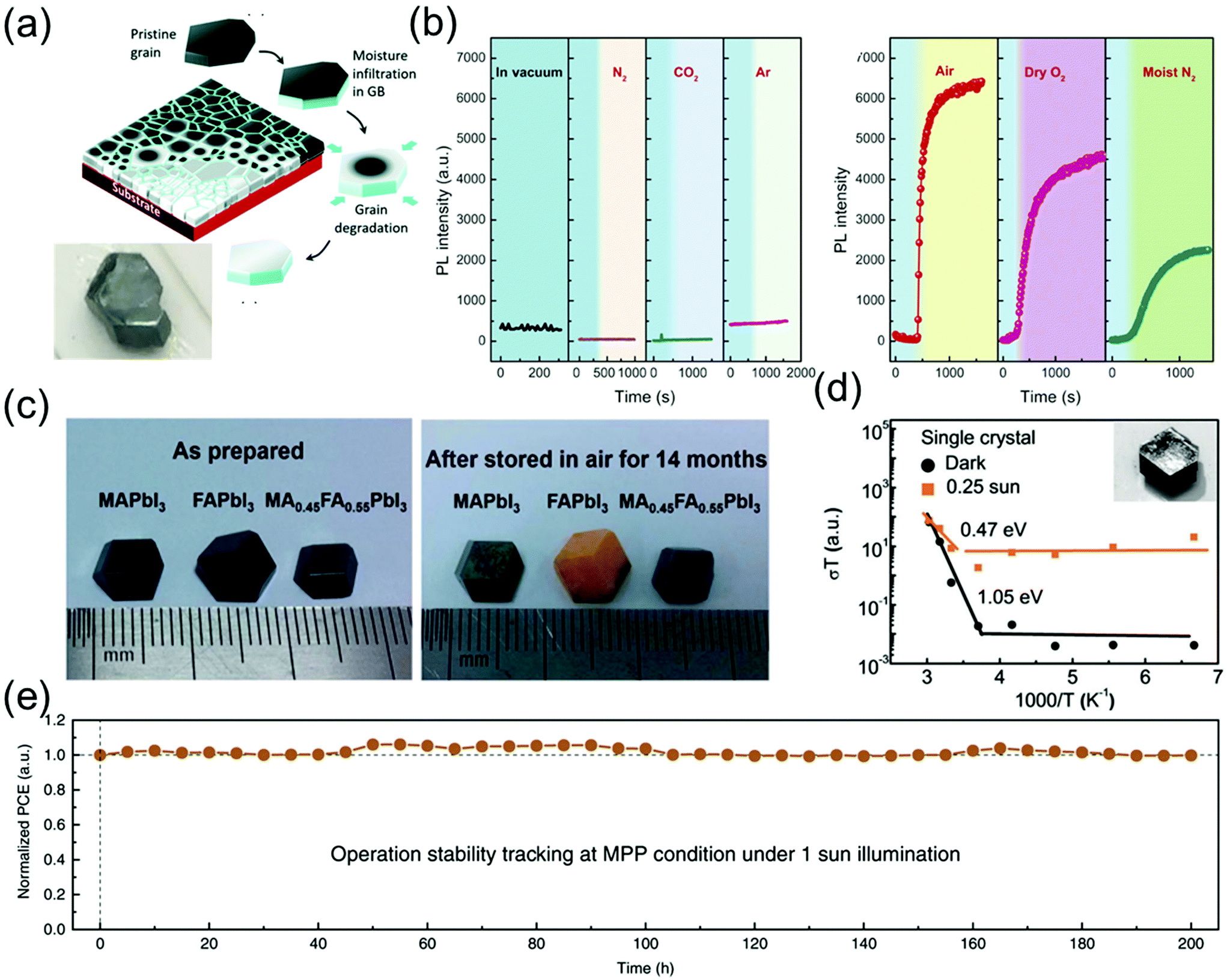
Because perovskite single crystals are free of grain boundaries and exhibit low defect densities, they can maintain their chemical structure and excellent properties in air for a long time. Although the stability of these crystals is superior to that of their polycrystalline counterparts,109 the stability of perovskite single-crystal-based commercial devices in ambient air is insufficient for an efficient device operation. Consequently, numerous efforts have been made to enhance the stability of single-crystal devices for various applications.According to a previous study, the MAPbI3 single crystals can maintain their metal-like surfaces in air for at least 6 months5 and a black-colored surface without any encapsulation and notable degradation in air for 2–3 years as shown in Fig. 14a.12 Wang et al.12 reported that the degradation always begins at the grain boundaries, resulting in a serious decline in the stability of both perovskite polycrystals and single crystals. Fig. 14a shows that the grain boundaries of perovskite polycrystalline films are composed of an amorphous intergranular layer, and the high density of carrier traps induces moisture-induced degradation along the in-plane direction, such that the degradation rate is proportional to the amount of grain boundaries. As a result, the scaling behavior of the degradation of MAPbI3 polycrystalline films as well as the excellent stability of single crystals against degradation suggest that the grain boundaries in perovskite materials play an important role in initiating the moisture-induced degradation process.
 | ||
| Fig. 14 (a) Schematic diagram showing degradation of MAPbI3 films in moisture, along the in-plane direction and photograph of the MAPbI3 single crystal stored in ambient air for 2–3 years. Reproduced with permission.12 Copyright 2017, RSC. (b) Effect of exposure to different gaseous environments on the PL intensity of MAPbBr3 single crystals. PL intensity as a function of time in vacuum and on exposure to dry N2, dry CO2, and dry Ar (left). PL intensity as a function of time on exposure to air, dry O2, and moist N2. In each panel, the blue shaded area indicates intensity recorded under vacuum (right). Reproduced with permission.53 Copyright 2016, AAAS. (c) Photographs of the as-prepared MAPbI3, FAPbI3, and MA0.5FA0.5PbI3 single crystals (left), and the same crystals after they were stored in air (relative humidity 45–55%) for 14 months (right). Reproduced with permission.55 Copyright 2017, RSC. (d) Temperature-dependent conductivity of the single crystals; the inset shows the SEM images of the test samples. Reproduced with permission.56 Copyright 2016, RSC. (e) Long-term stability under continuous output at maximum power point (MPP) condition (1 Sun). Reproduced with permission.57 Copyright 2020, Springer Nature. | ||
Fang et al.53 reported the PL intensity variation of perovskite single crystals as a function of time under various environmental conditions such as gas atmosphere (N2, CO2, and Ar) and moisture. Although the PL intensity of the MAPbBr3 perovskite single crystals was not affected by the dry gases, air, dry O2, and moist N2 drastically increased the PL intensity as shown in Fig. 14a. The PL intensity of perovskite single crystals varied more significantly in air than in dry O2 and moist N2, which implies that molecular gases such as O2 and H2O vapors enhance the PL intensity. Although the interaction between the gas molecules and defects is weak, i.e., the gas molecules are physisorbed at the defect sites, it can induce changes in the optical emissions of perovskite single crystals.
Li et al.55 grew three species of perovskite single crystals, namely MAPbI3, α-FAPbI3, and MA0.45FA0.55PbI3, through a modified ITC method. As shown in Fig. 14c, the three as-grown 8 mm single crystals exhibited rhombohexagonal dodecahedron or rhombic dodecahedron shapes with metallic black color. After exposure to air with 45–55% relative humidity for 14 months, the MA0.45FA0.55PbI3 single crystals still maintained their original black color, whereas the color of the α-FAPbI3 single crystals changed to yellow and the MAPbI3 single crystals exhibited yellow spots on the surface. This result indicates that the single crystals with mixed cations showed a superior long-term stability, compared with the MAPbI3 and FAPbI3 single crystals.
Xing et al.56 investigated the influence of light on ion migration in both polycrystalline films and single crystals, by measuring the activation energy from ion conduction under both dark and light conditions. Fig. 14d shows that the ion-migration-influenced activation energies of the single crystals are 1.05 and 0.47 eV under dark and 0.25 Sun illumination. These values are at least two-fold larger than those of the polycrystalline films (05 eV in the dark and 0.14 eV under 0.25 Sun illumination). These results confirmed that light illumination decreases the ion-conduction-influenced energy barrier along the polycrystalline grain boundaries and single-crystal surfaces. A large number of grain boundaries facilitate the formation of a large number of ion migration channels with lower energy barriers, according to Wang et al.12 Notably, the ion migration in polycrystalline perovskites could be significantly activated by illumination, whereas the activation energy in single crystals is too large to cause any notable ion migration.
Song et al.57 reported the long-term stability of photovoltaic operation in perovskite single crystals under 1 Sun illumination in a glovebox without any cooling stage. An ultrathin MAI layer was developed to optimize the anode contact via surface treatment, leading to the passivation effect. This drastically enhanced the open circuit voltage (VOC) and fill factor (FF) in perovskite solar cells with lateral structures. The best performing cell achieved an efficiency of 11.52% under 1 Sun condition, without any obvious hysteresis effect. Fig. 14e shows variations in the device performance under 200 h continuous operation. Evidently, the best device still maintained 99.77% of its properties after this long-term operation. Thus, enhancing the stability of perovskite single crystals via crystal and structural engineering can provide a potential pathway for further applications of these materials.
5. Optoelectronic device applications
This section discusses device applications of halide perovskite single crystals in various fields, including solar cells, photodetectors, LEDs, lasers, and flexible electronics. These single-crystal application technologies are classified according to the type of device and recent research results.5.1. Solar cells
Perovskite solar cells have recently emerged as cost-effective and energy-efficient candidates to replace or supplement existing solar technologies such as silicon and GaAs. In this technology, polycrystalline films are leading in terms of efficiency. In theory, single crystal perovskites have lower defect density and longer carrier diffusion lengths than do the polycrystalline films, providing an opportunity to overcome the limitations of polycrystalline thin films and get as close as possible to the Shockley–Queisser limit. However, because of thickness control and the general device-compatible solution-growth conditions, a few groups are leading the development of single-crystal-based perovskite solar cells.Peng et al.30 simply fabricated solar cells by evaporating Au electrodes onto the surface of single-crystalline MAPbBr3 films on ITO or FTO/TiO2 as shown in Fig. 15a. The apparent rectification of the current density–voltage (J–V) of the cell was corroborated the potential of single-crystalline film-based devices. The performance of solar cells was investigated with a power conversion efficiency (PCE) of 6.53%, a VOC of 1.36 V, a short-circuit current (JSC) of 6.96 mA cm−2, and an FF of 0.69, for a best device made of a 1-μm thick perovskite crystal. The trap densities in single crystalline and polycrystalline perovskites were crucial to understanding the efficiency of solar cells. Ni et al.110 first performed the trap density distribution by using the DLCP method for a high-performance perovskite thin-film solar cell having a device structure of ITO/poly(triarylamine) (PTAA)/Cs0.05FA0.70MA0.25PbI3/C60/BCP/Cu with VOC, JSC, FF, and PCE of 1.15 V, 23.4 mA cm−2, 77.3%, and 20.8%, respectively, as shown in Fig. 15b. The measured trap density distribution in thin film showed similar trap distribution capabilities, where most deep trap states are located near single-crystalline interfaces. From the simulation, the PCE of a thin and bulk MAPbI3 single-crystal solar cell could be further improved to 25.4% and 26.8% if the interface trap density was reduced. Such single-crystalline perovskite films were constructed the inverted p–i–n planar solar cells.
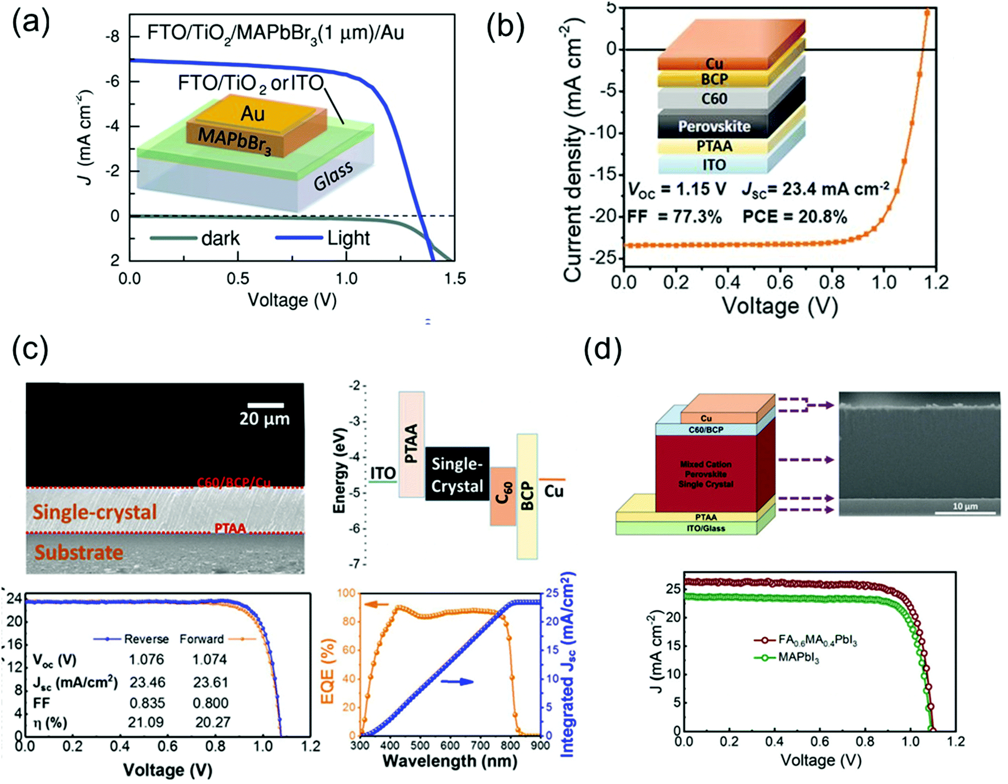 | ||
| Fig. 15 (a) Dark and illuminated J–V curves and an illustration of the device architecture of FTO/TiO2- and ITO-based single-crystalline solar cells. Reproduced with permission.30 Copyright 2016, Wiley-VCH. (b) Cs0.05FA0.70MA0.25PbI3 thin-film solar cells. Reproduced with permission.110 Copyright 2020, AAAS. (c) Cross-sectional SEM image of an MAPbI3 single crystalline solar cells and the corresponding energy level diagram. J–V curves of the champion cell in forward- (orange) and reverse-scans (blue) and the corresponding photovoltaic parameters under 1 Sun illumination. EQE spectra with the integrated JSC of the champion cell. Reproduced with permission.36 Copyright 2019, ACS. (d) Device architecture of single-crystalline solar cell, and the corresponding cross-sectional SEM image. J–V curve of the single-crystalline MAPbI3 and FA0.6MA0.4PbI3 solar cells under 1 Sun illumination. Reproduced with permission.35 Copyright 2021, RSC. | ||
Chen et al.36 grew MAPbI3 single crystals without pinholes and grain boundaries using a simple solution space-limited inverse temperature crystal growth method for use as an active layer of solar cells. The device structure, ITO/PTAA/MAPbI3 single-crystal/C60/BCP/Cu, with the cross-sectional scanning electron microscopy (SEM) image and the corresponding energy band diagram are shown in Fig. 15c. The J–V characteristics under 1 Sun illumination presented the photovoltaic parameters of the best cell. The PCE, JSC, VOC, and FF were 21.09%, 23.46 mA cm−2, 1.076 V, and 83.5%, respectively. The smooth surface can completely cover the charge transport layer, preventing direct contact between crystals and metals and decreasing the significant reduction in photovoltaic parameters due to material failure, for example, cracks in the absorber. Alsalloum et al.35 also fabricated the single-crystalline perovskite solar cell consisting of ITO/PTAA/FA0.6MA0.4PbI3/C60/BCP/Cu as shown in Fig. 15d. The thin perovskite absorber layer with a 15 μm-thick thin single crystal is presented in the cross-sectional SEM image. As a result of the mixed cation, the reduction of bandgap led to a redshift in the band edge by 30 nm, which resulted to increase the JSC about 2 mA cm−2 compared with the previous high-performance MAPbI3 perovskite single-crystal solar cells. Despite the decrease in the bandgap, the VOC did not decrease. The VOC value compared with that of the MAPbI3 single-crystal-based device manufactured with the same solvent (GBL) was almost the same.36 The PCE, JSC, VOC, and FF of the best device was achieved as 22.8%, 26.2 mA cm−2, 1.1 V, and 0.79, respectively.
5.2. Photodetectors
As a superstar material for solar cell applications, the perovskite is also being recognized as an amazing material for photodetectors. Single-crystalline perovskite materials show lower carrier concentrations than polycrystalline films for photodetectors, which are an essential for imaging sensors and photodetectors requiring low dark current and high ON/OFF ratio. In addition, high carrier mobility combined with low trap density will render high response time and high external quantum efficiency (EQE); both are major success values for imaging, photosensor, and optoelectronic detecting applications, including photodetectors,39,60,121,122 X-ray detectors,40,71,123 and γ-ray detector.124Influenced by the excellent optoelectronic characteristics, including high carrier mobility, small trap density and long carrier life, Liu et al.33 fabricated imaging sensor applications using high-quality MAPbBr3 single crystals. The 7 × 8 photosensor array on the MAPbBr3 single-crystal wafer consisted of five interdigit grid lines with Cr/Au pads. The I–V curves of the single-crystal device were measured in a dark state and under 525 nm wavelength illumination with a light intensity of 3–60 mW cm−2, as shown in Fig. 16a. The measured dark current (Idark) was as low as 10−9 A, while it increased to 10−4 A under 60 mW cm−2 illumination, making it more than five times larger than the dark current. At the same illumination, the photocurrent (Iphotocurrent) of the microcrystalline MAPbBr3 thin film device was only 10−7 A, about 1000 times smaller. As the relation between the Iphotocurrent and Idark is related to the performance of the device, the responsivity (R), EQE, and detectivity (D*) was determined. R is defined as the ratio of photocurrent generated to the incident light, EQE is defined as the number of carriers produced by an external circuit for each incident photon, and D* is generally used as a shot noise from the dark current reflecting the sensitivity of a photosensor. The R, EQE, and D* of best device were calculated as 1.6 × 10⁴ mA W−1, 3900%, and 6 × 10¹³ Jones, respectively. The response speed was also ultrahigh at 40 μs, and the photoresponse stability was remarkable for 35 days of exposure in ambient air. The excellent performance parameters of uniformity, high detectivity, fast response, and long-term stability were better than those of the single-crystalline silicon or InGaAs.
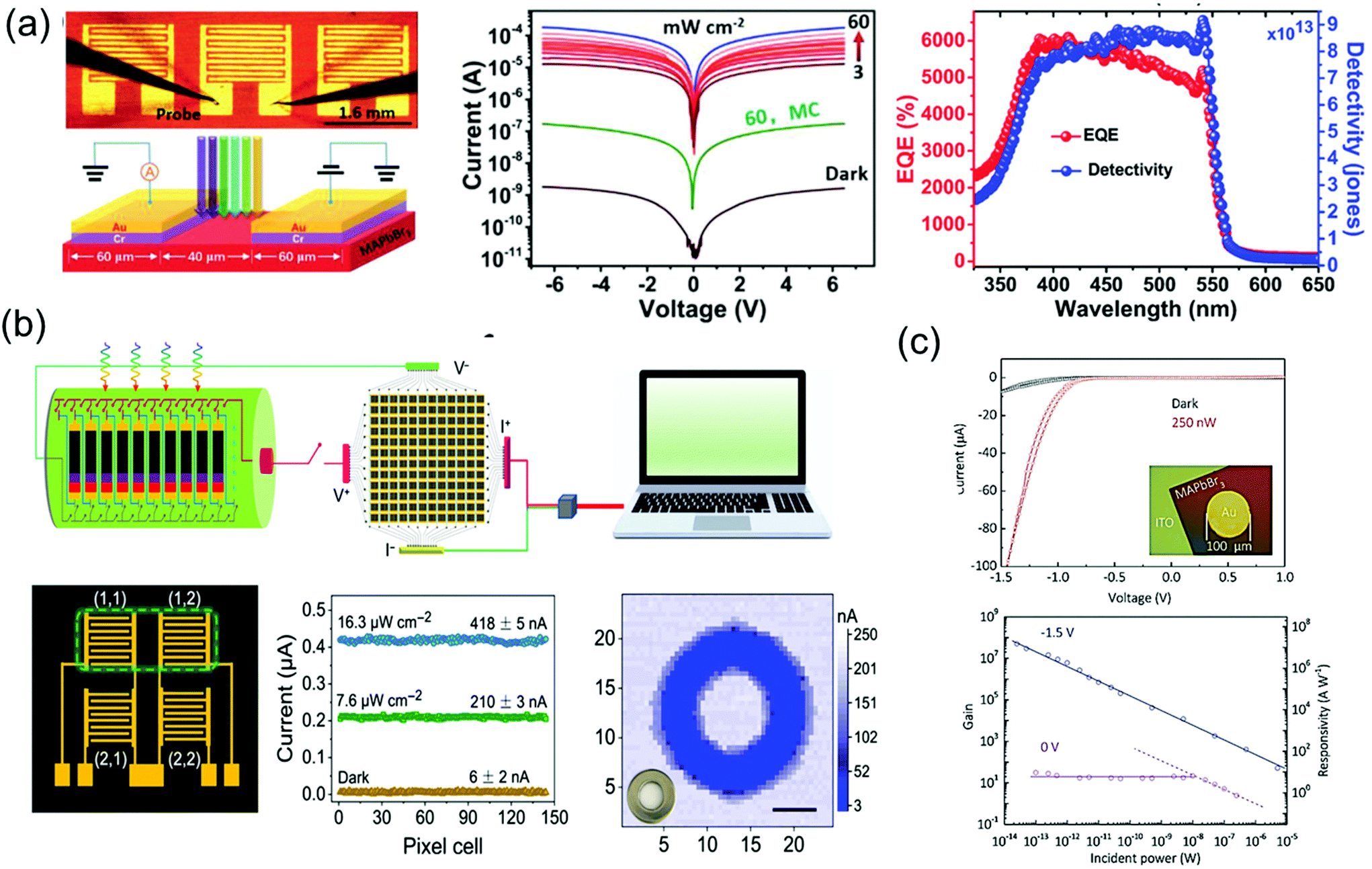 | ||
| Fig. 16 (a) Image of the fabricated MAPbBr3 single-crystal photodetector, and the schematic of the device operation. I–V characteristics measured under dark and light conditions various intensities. EQE and detectivity (D*) of the MAPbBr3 single-crystal photosensor under a 4 V bias. Reproduced with permission.33 Copyright 2015, Springer Nature. (b) Schematic illustration of the measurement of the 2% FAH FAMACs single-crystal-integrated photodetector array for optical imaging. Detailed illustration and photocurrent responses of a 2 × 2 pixel matrix photodetector under illumination. Photograph and corresponding three-dimensional current map of a metal annular ring, imaged by a single-pixel device; scale bar: 5 mm. Reproduced with permission.125 Copyright 2021, AAAS. (c) I–V curves under dark and light conditions. Gain and responsivity of the photodetector and optical image of the device (inset). Reproduced with permission.126 Copyright 2018, Wiley-VCH. | ||
Liu et al.125 also fabricated the integrated 12 × 12 array of a phase separation-suppressed (FAxMAyCs1−x−y)Pb(IzBr1−z)3 single-crystal photodetector by using the reductant as shown in Fig. 16b. The use of formic acid, as a reductant, inhibited phase separation by reducing the oxidation of the iodide ions and cation deprotonation while growing FAMACs perovskite single crystals. Single crystals grown in this way have excellent optoelectronic characteristics, making it possible to produce successful high-performance photodetectors with the device structure of Au/FAMACs single crystal/C60/BCP/Au. The best device exhibited large R of 598.6 A W−1, excellent D* of 6.7 × 10¹⁴ Jones, and a fast response speed of 0.88 μs.
Good crystallinity and appropriate thickness of macroscale single crystals were limited by the rate of isotope growth in the solution. Recently, the spatially limited growth method has been introduced to grow single-crystalline perovskite thin film with an improved aspect ratio. Yang et al.126 fabricated the single-crystalline MAPbBr3 thin film photodetector by depositing a circular Au electrode on MAPbBr3 grown on an ITO substrate, as shown in Fig. 16c. Owing to the MAPbBr3/Au Schottky-diode structure, the I–V curves under dark and light conditions showed rectifying behavior. When a negative bias was applied, the diode was open due to the formation of the Schottky barrier at the interface. At negative bias of 1.5 V, the current increased clearly due to incident light. The obvious response came from the carrier density increases in MAPbBr3 under illumination or trapped photon-excited electrons at the interface due to the height of Schottky barrier. The resulting photoconductive gain was calculated to have a maximum value of 5.0 × 10⁷ at an external bias of −1.5 V and an incident power of 25 fW. The largest R and the corresponding D* of the best device are 1.6 × 10⁷ A W−1 and 1.3 × 10¹³ Jones.
5.3. Light-emitting diodes
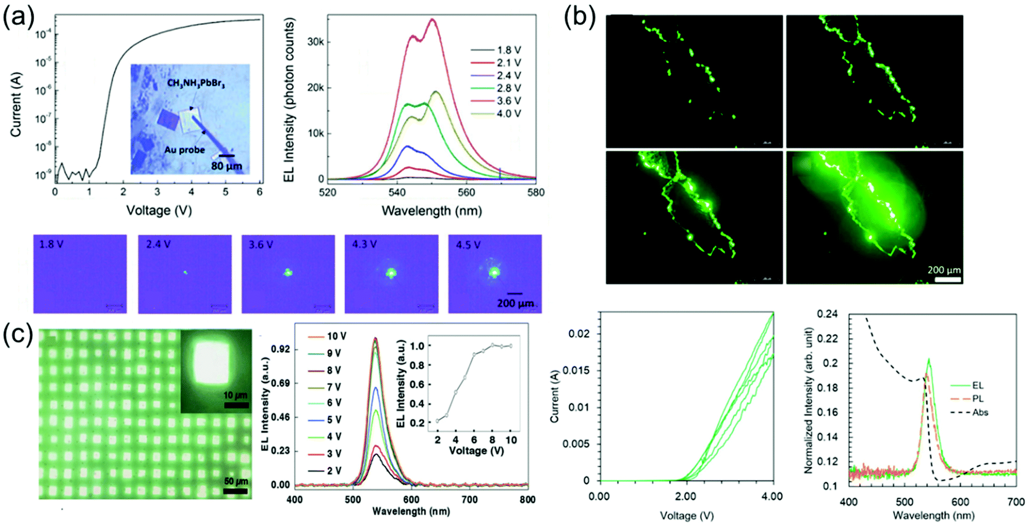
Perovskite-based LEDs are emerging as ideal candidates for next-generation lighting technology with their excellent photoelectric characteristics such as high PL quantum yield (PLQY, about 100%), narrow bandwidth (<20 nm), and easy wavelength tuning in the entire spectrum of visible light (400 to 800 nm).127–138 Over the past 5 years, the perovskite LED's external quantum efficiency (EQE) has increased from 0.1 to more than 20%, making it a platform with remarkable potential.139–142 Recent advances in perovskite LEDs are based on types of perovskite crystal including three-dimensional perovskites, two-dimensional or semi-two-dimensional perovskites, and perovskite nanocrystals.Single-crystalline perovskite microplatelets were a type of three-dimensional perovskite crystal that can be used to produce single-crystalline LEDs. Chen et al.43 fabricated the simple MAPbBr3 microplatelet crystals-based LED with ITO on glass as the anode and Au film as the cathode. Fabricated LEDs were activated without using any electron injection layer or a hole injection layer. Optical images of the operating LEDs under different applied bias and corresponding emission spectra are shown in Fig. 17a. The light emission intensity was increased according to the applied bias from 1.8 to 3.6 V, but rather decreased at 4.0 V. Such reduction in emission intensity at a high bias voltage was likely due to the decrease in light collection efficiency as photons emitted from the side surface increase. Two peaks as 542–544 nm and 548–551 nm can be identified in electroluminescence spectra. This is due to the exciton–exciton scattering process. The relative intensity improvement of the 548–551 nm peak as the bias voltage increases after 2.4 V indicates that the exciton–exciton scattering process becomes more important at a high injection current density. This was related to the enhanced exciton–exciton scattering at high exciton density, showing a red shift for the second emission peak after 2.8 V.143 It is worth noting that exciton–exciton scattering was used as a mechanism to realize stimulated light emission at a low excitation threshold, such as zinc oxide semiconductor thin films.144 As a result, an efficient and stable perovskite LED was achieved at 1.8 V of bias voltage and maintained for at least 54 h without degradation with a luminance of about 5000 cd m−2.
 | ||
| Fig. 17 (a) I–V characteristics and a microscopic optical image of a fabricated LED. Electroluminescence spectra at different applied voltages. Microscopic optical images of the LEDs at different applied voltages. Reproduced with permission.43 Copyright 2017, ACS. (b) Optical images showing the pure green luminescence emitted by the MAPbBr3 single-crystal LEDs with increasing bias voltage from 2 to 4 V. Forward and backward I–V curves measured in three cycles. The absorption (black, dashed), PL (orange, dashed), and electroluminescence (green, solid) spectra of the fabricated LED. Reproduced with permission.44 Copyright 2018, IOP Publishing. (c) Optical images showing the emission of LED arrays. Normalized electroluminescence intensity as a function of the drive voltage. The emission peak does not shift, showing that the recombination region does not change under different drive voltages. The electroluminescence intensity saturates at around 8 V. Reproduced with permission.149 Copyright 2018, Wiley-VCH. | ||
Nguyen et al.44 fabricated a simple ITO/MAPbBr3 single-crystal/ITO device by using the cast capping method as shown in Fig. 17b. When a bias voltage from 2 to 4 V was applied to the top and bottom ITO electrodes of the fabricated device, electroluminescence was not observed because carriers were hardly injected due to the high energy barrier of ITO at low bias voltage. As the applied bias voltage increases, electroluminescence began to be noticeably detected at the crystal edge and corner. At 2 V, the current started to increase, indicating carrier injection into a single crystal. Therefore, the forward and backward currents gradually decreased, while the small hysteresis remained in the repeating cycle. The cause of the decrease in current may be damage in the crystals due to Joule heating. In particular, the crystal structure was noticeably degraded at a high bias voltage. The weak peaks in the absorption spectrum near the band gap were found to be affected by the excitonic transition from the in-gap defect states. Depending on such a spectrum, the optical band gap of the single crystal becomes 2.25 eV, which is larger than the bulk crystal and smaller than the polycrystalline thin film. Simple ITO/MAPbBr3/ITO devices prevent absorbance and emission from the transport of electrons and holes, so eliminating the interface between a single crystal and this transport layer. Therefore, this results from the intrinsic characteristics of MAPbBr3 single crystal. Electroluminescence showed a slight red shift of about 0.02 eV compared with PL. de Quilettes et al.145 mentioned that such red-shifted electroluminescence can come from shallow trapping levels at grain boundaries. However, the large carrier diffusion length of the perovskite is suggestive of low defect density, reducing the number of non-radioactive trapping paths.22,28,146 On the other hand, although an increase in the number of defects was concentrated on the grain boundaries acting as a nonradiative recombination path, radiative recombination may be improved by reducing the size of grains due to strong spatial confinement.147,148 These results suggested that the carrier generates excitons after being allocated at the grain boundary. The carrier was probably diffused and concentrated at the crystal edge. As a result, electrons and holes met to form excitons with a high probability and the device showed pure green light with a low operating voltage of 2 V and a narrow half width of about 20 nm.
In Fig. 17c, an LED array with chemical epitaxial growth of single-crystal MAPbBr3 is shown. Lei et al.149 fabricated growth rate-controlled epitaxial MAPbBr3 single crystals with the poly(3,4-ethylenedioxythiophene):poly(styrenesulfonate) (PEDOT:PSS) layer. Due to the high crystal quality in a green LED array in which each crystal operated as a single pixel, the emission intensity of each crystal was uniform. The color of the individual pixels became almost white due to their high emission intensity. The electroluminescence intensity at various voltages at room temperature increased when the driving voltage was increased without an emission peak shift, indicating the absence of radiative decay.150 The dominant emission peak was about 540 nm, and the full width at half maximum was about 30 nm. Integrated electroluminescence intensities under different driving voltages tended to saturate from 8 V and slightly decreased at 9 and 10 V, which may be due to inevitable heating effects at high current density levels.151 The turn-on voltage for each device showed some variability, but most devices had a low turn-on voltage of 2 to 3 V. The maximum EQE of 6.1% was achieved at 9.0 V, which is greater than that of similar devices using polycrystalline materials.152,153 As the applied voltage and current density increased, the increase in EQE suggests that a high density of charges is required for efficient radiation recombination. The epitaxial single crystal shows improved carrier dynamics compared with the polycrystalline thin film shown in the single-crystal LED array.
5.4. Lasers
Metal halide perovskite materials can be used in advanced microlaser technology such as compact nanophotonics design and near-wavelength lasers because of two or more large refractive indices and defect-tolerant materials. In these materials, defect sites are placed very close to the conduction or valence bands.127,154–158 In addition, halide perovskites provided excitons at room temperature and yielded light-emitting quantum efficiency in the range of tens of percent. Various perovskite microlasers were fabricated through a low-cost approach and generated laser emission in the range of 420 to 825 nm.159–162 Among various types of perovskite microstructures, solution/steam self-assembled or engineering-processed polygonal, circular and spherical micro/nano single-crystal perovskites were developed as whispering gallery mode-type micro/nano lasers to exhibit high lasing performance such as low threshold value, high quality (Q) factor, and high optical gain.46,163–167 This amazing lasing performance is closely related to the low trap density and large optical absorption of high-quality perovskites.Liao et al.46 fabricated single-crystalline square microdisks MAPbBr3 by using a one-step solution self-assembly method for whispering gallery mode microdisk lasers. Broad spontaneous emission at 545 nm was observed at a low excitation density of P = 2.4 μJ cm−2 indicating a full width at half maximum (FWHM) of 23 nm. When the excitation density was increased from 3.6 to 5.4 μJ cm−2, a single peak gradually appeared at about 557.5 nm, and finally became dominant. In particular, FWHM = 1.1 nm of this peak is much narrower than FWHM = 23 nm of spontaneous emission, and also narrower than an amplified spontaneous emission of FWHM = 10 nm observed in a 65 nm-thick MAPbBr3 thick film without cavities, indicating the observation of lasing emission. Single-mode racing at 557 nm is achieved based on a whispering gallery mode micro-resonator built in at room temperature. The fabricated microdisk laser was highly emissive in the solid state, and its high PLQY was confirmed as 22% ± 5%, which is slightly higher than 17% of nanoparticles due to the low defect density of the single-crystalline microdisk.168 By partially substituting Br with Cl, the laser wavelength is continuously adjusted from 525 to 557 nm.
Zhizhchenko et al.47 proposed the fabrication of perovskite microlasers through femtosecond laser ablation using donut-shaped laser beams, as shown in Fig. 18b. Structured light was optimized by its charges that can implement various diameters of microdisk up to 2 μm. The proposed microdisk printing method allowed manufacture of a single-mode perovskite microlaser that operates with a maximum Q factor at room temperature. Most of the processed perovskite microdisks showed single-mode lasing due to a certain level of roughness at the edge. Ultrashort pulses allowed soft ablation at clean and soft edges without damaging microdisk bulk and reducing material gains. As a result, minimum lasing thresholds for nanosecond (150 μJ cm−2) and femtosecond (7 μJ cm−2) optical pumps were observed.
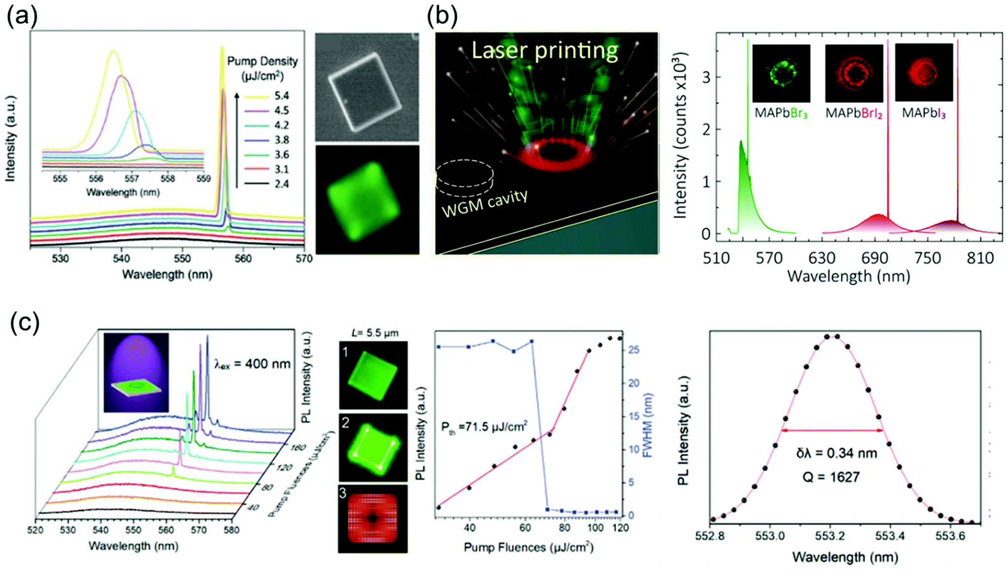 | ||
| Fig. 18 (a) PL spectra of a square-shaped microdisk with a footprint of 2.0 × 2.0 × 0.6 μm3 as shown in the optical and PL intensities measured as a function of excitation density at 400 nm. Inset is the enlarged PL spectra between 555 and 559 nm. Reproduced with permission.46 Copyright 2015, Wiley-VCH. (b) Schematic of the large-scale arrays of perovskite microlasers and their photoexcitation. Optical images of the perovskite microlasers of different compositions and their lasing spectra: MAPbI3 (brown curve), MAPbBrI2 (red curve), and MAPbBr3 (green curve). Reproduced with permission.47 Copyright 2019, ACS. (c) Pump-fluence-dependent PL spectra of a single FAPbBr3 square-shaped microdisk with edge length (L) of ≈5.5 μm under 400 nm (1 kHz, 100 fs) excitation. The inset shows schematic of an FAPbBr3 square-shaped microdisk on a glass substrate, pumped by a 400 nm excitation wavelength. Fluorescence images of (1) below and (2) above the lasing threshold. (3) Simulated electric-field distribution, |Hz|, inside the square-shaped perovskite cavity under a transverse electric resonant mode. Pump-fluence-dependent PL intensity and FWHM of a lasing oscillation mode at 553.2 nm. Reproduced with permission.48 Copyright 2020, Wiley-VCH. | ||
In addition, Li et al.48 developed solution-processed square and quasi-circular FAPbBr3 microdisks for facet-formed whispering gallery mode lasers as shown in Fig. 18c. For the one-photon pumped lasing performance, a PL peak at 542 nm was observed at a low pump flow rate, and the FWHM was 27 nm. As the pump flow rate increased, a rapid emission peak appeared at 553.2 nm, indicating the occurrence of a single-mode lasing action. The red shift of the lasing peak was related to reabsorption during one-photon pumping racing.169 Since the lasing action of the square microdisk mainly occurred in the whispering gallery mode under uniform excitation, the additional light emission from the corners and the edges of the square microdisk was caused by lasing light coupling. A linear increase in the PL peak intensity at a low pump fluence was affected by a spontaneous emission process. At a high pump fluence, the pump fluence-dependent PL peak intensity changed to a hyperlinear increase, and further linear increase occurred from amplified spontaneous emissions and lasing processes. As a result, the one-photon pumped lasing threshold of the FAPbBr3 square microdisk was 71.5 J cm−2, and the average threshold carrier density was determined to be 6.1 × 1018 cm−3. The FWHM of the lasing peak close to the threshold was 0.34 nm, corresponding to the Q factor of 1627.
5.5. Flexible applications
Flexible devices are attracting attention as next-generation application devices such as foldable displays, biomedical imaging systems, and wearable devices.170–175 Recently, perovskite material-based flexible solar cells, photodetectors, image sensors, and wearable equipment have been widely reported. However, the stiff and brittle properties of single-crystal materials are not easily compatible with the use of flexible elements. The mechanical properties of the material can be greatly improved when the size is reduced to nanometer.176–178 In the following, reports to realize a high-performance flexible application using a very thin single-crystalline perovskite film grown on a flexible substrate are summarized.Gu et al.49 fabricated a perovskite single-crystal wearable light-emitting device-embedded polydimethylsiloxane (PDMS) film by using inkjet printing, as shown in Fig. 19a. The liquid PDMS precursor was a key element having a spatial confined effect in the fabrication of a perovskite single-crystal array, which effectively delayed the crystallization process and promoted the formation of a single-crystal perovskite structure in the PDMS, hence effectively fabricating a flexible device. In order to adapt to the light-emitting application, it is important to manufacture various perovskite fluorescent patterns of wafer sizes.179,180 In particular, the strategy of preparing large fluorescent perovskite single-crystal patterns through inkjet printing directly inside PDMS films has the advantage of being a light-emitting application designed through fluorescent images of macroscopic letters “printed” with bright green emissions at centimeter scale. It was confirmed that the perovskite single crystal has the advantage of having excellent homogeneity and reproducibility of bright green fluorescence at a 533 nm PL peak. The pattern printed on the flexible substrate shows that the flexible properties are maintained. The perovskite single-crystal pattern made of such inkjet is efficient and costs less than that of micro-manufacturing technology. All these patterns are transparent, flexible, and stable in the surrounding environment, indicating a variety of applications, such as wearable light-emitting devices and flexible panel displays.181,182
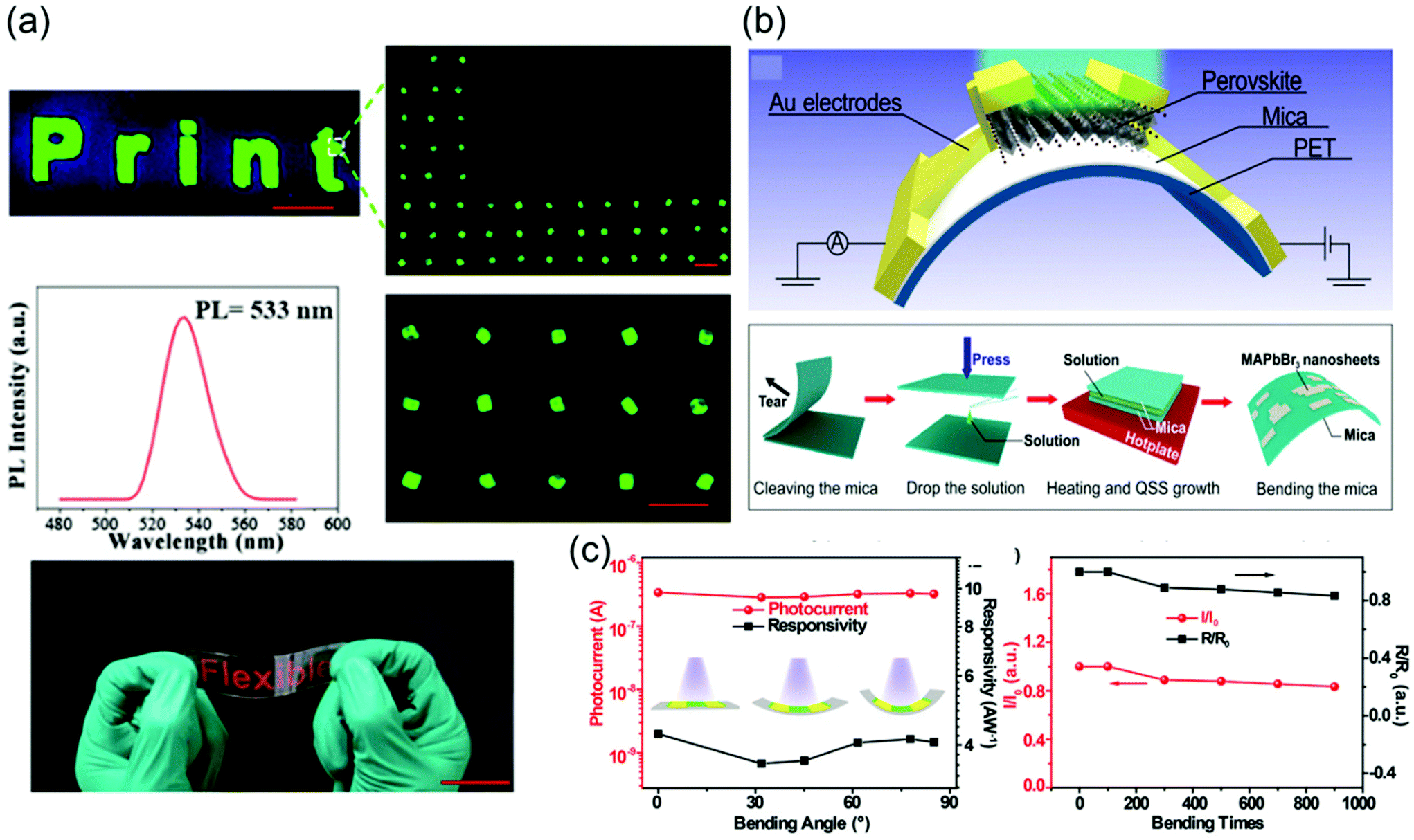 | ||
| Fig. 19 (a) Fluorescent pattern image fabricated with the perovskite prepared using the PDMS film with the inkjet-printed macroscopic letters “Print,” and PL spectrum of the perovskite fluorescent pattern-embedded PDMS film. Reproduced with permission.49 Copyright 2020, ACS. (b) Schematic of the architecture of the fabricated flexible photodetector and the solution-growth steps. Reproduced with permission.50 Copyright 2021, ACS. (c) Performance of the device depending on the bending degrees and bending cycles at a bias voltage of 1 V. Reproduced with permission.51 Copyright 2020, Wiley-VCH. | ||
In addition to the light-emitting element, a flexible photodetector using a single perovskite crystal has been proposed. Jing et al.50 fabricated the flexible photodetector by using ultrathin single-crystalline MAPbBr3 film on flexible polyethylene terephthalate (PET) substrate with an interlayer of atomic scale of thin mica, as shown in Fig. 19b. The mica sheet acted to support the growth of thin single-crystal membranes. The mica sheet had a smooth surface, excellent wettability, and a low chemical activity for promoting lateral growth and expanding crystal sheets.183–185 Also, the trap state density of nanosheets is about 2.6 × 1011 cm−3 based on the space charge limit current analysis, which is much lower than polycrystalline perovskite thin films.30,186 As a result, the fabricated flexible photodetectors made of single-crystal perovskites with a thickness 20 nm showed high reactivity of 5600 A W−1, and no visible degradation in photocurrent and on/off switching ratios was observed after 1000 bending cycles.
Li et al.51 fabricated MAPbBr3 single-crystal microwire arrays photodetectors by using an in situ encapsulation method, as shown in Fig. 19c. The photodetector was manufactured by evaporating a gold electrode with a thickness of 200 nm and an interval width of 100 mm into MAPbBr3 single-crystal microwire arrays on flexible PET substrate. The high crystal quality of the MAPbBr3 single-crystal microwire array was demonstrated by the performance of the device. The performance of the device showed a high detectivity up to 4.1 × 10¹¹ Jones and fast response time of 1.6 ms for rise and 6.4 ms for decay. While the device was in bent state the performance of the device did not decrease significantly. The device was proved to be durable, and maintained more than 80% photovoltaic and responsiveness after 900 bending cycles.
6. Conclusion and perspective
In this review, the crystallization techniques for synthesizing perovskite single crystals, including advanced methods, are summarized, and the optoelectronic properties of such crystals are analyzed based on various characterization methods. The outstanding advantages of perovskite single crystals, viz. an enhanced carrier transport, highly efficient light-harvesting capability, and excellent stability, are crucial for the optoelectronic applications of these materials. The current challenges and perspectives on further development of this promising research field are highlighted as follows:(1) Low-toxicity Pb-free perovskite and green solvent for fabrication of single crystals: although Pb-based halide perovskites are used to fabricate the most efficient optoelectronic devices, the toxicity of Pb restricts the commercialization of perovskite single crystals. Therefore, alternative Pb-free perovskite single crystals are required for developing eco-friendly devices. Ke et al.187 reported alternative Pb-free halide perovskites such as Sn- or Ge-based perovskites. Although Sn and Ge are not the ideal substitution materials because of their poor stability, devices fabricated using Sn + Ge-based perovskites are expected to exhibit an efficient performance. In addition, the growth of Pb-free perovskite single crystals should be pursued because of their device-oriented properties such as good stability, tunable bandgaps, and controllable morphologies.
(2) Epitaxial growth and strain engineering: solution-based epitaxial growth has been employed to form stable interfacial bonds with perovskite single-crystal substrates. Solution-based epitaxy facilitates a large growth coverage because of the formation of a uniform interface between the substrate and the precursor. By tailoring the composition or designing lattice mismatch, strain engineering can be applied to change the crystal structure or effective mass, resulting in an enhanced hole mobility in FAPbI3, as demonstrated by Chen et al.188 Additionally, the applied strain can enhance the stability of metastable perovskites, exhibiting potential for high-performance device applications.
(3) Expansion of applications: beyond various optoelectronic devices, perovskite single crystals have been used as photocatalysts, and implemented as highly stable photocathodes for water splitting.189 With various electron and hole transfer layers or structural configurations, perovskite single-crystal photocatalysts show an excellent development potential. Recently, perovskite single crystals have been exploited as artificial synapses for realizing neuromorphic and bioinspired intelligent systems.190 MAPbBr3 single-crystal thin platelets exhibit all the essential synaptic behaviors such as paired-pulse facilitation, spike-dependent plasticity, transition from sensory memory to short-term memory, and potentiation/depression. The synaptic devices based on perovskite single crystals could provide a new direction for future neuromorphic bioelectronics.
Conflicts of interest
There are no conflicts of interest to declare.Acknowledgements
This research study was supported by the Basic Science Research Program through the National Research Foundation of Korea (NRF) funded by the Ministry of Education (NRF-2018R1A6A1A03025340 and NRF-2020R1I1A1A01068700) and by the Ministry of Science, Technology, and ICT & Future Planning (NRF-2021R1A2B5B02001961).References
- Y. Zhang, Y. Liu, Y. Li, Z. Yang and S. Liu, J. Mater. Chem. C, 2016, 4, 9172–9178 RSC.
- M. M. Lee, J. Teuscher, T. Miyasaka, T. N. Murakami and H. J. Snaith, Science, 2012, 338, 643–647 CrossRef CAS PubMed.
- A. A. Zhumekenov, M. I. Saidaminov, M. A. Haque, E. Alarousu, S. P. Sarmah, B. Murali, I. Dursun, X.-H. Miao, A. L. Abdelhady, T. Wu, O. F. Mohammed and O. M. Bakr, ACS Energy Lett., 2016, 1, 32–37 CrossRef CAS.
- A. H. Slavney, T. Hu, A. M. Lindenberg and H. I. Karunadasa, J. Am. Chem. Soc., 2016, 138, 2138–2141 CrossRef CAS PubMed.
- Q. Dong, Y. Fang, Y. Shao, P. Mulligan, J. Qiu, L. Cao and J. Huang, Science, 2015, 347, 967–970 CrossRef CAS PubMed.
- G. Xing, N. Mathews, S. Sun, S. S. Lim, Y. M. Lam, M. Grätzel, S. Mhaisalkar and T. C. Sum, Science, 2013, 342, 344–347 CrossRef CAS PubMed.
- L. Etgar, P. Gao, Z. Xue, Q. Peng, A. K. Chandiran, B. Liu, M. K. Nazeeruddin and M. Grätzel, J. Am. Chem. Soc., 2012, 134, 17396–17399 CrossRef CAS PubMed.
- S. D. Stranks, G. E. Eperon, G. Grancini, C. Menelaou, M. J. P. Alcocer, T. Leijtens, L. M. Herz, A. Petrozza and H. J. Snaith, Science, 2013, 342, 341–344 CrossRef CAS PubMed.
- K. Shen, J. Hu, Z. Liang, J. Hu, H. Sun, Z. Jiang and F. Song, Crystals, 2018, 8, 232 CrossRef.
- H. Min, D. Y. Lee, J. Kim, G. Kim, K. S. Lee, J. Kim, M. J. Paik, Y. K. Kim, K. S. Kim, M. G. Kim, T. J. Shin and S. Il Seok, Nature, 2021, 598, 444–450 CrossRef CAS PubMed.
- M. A. Green, E. D. Dunlop, J. Hohl-Ebinger, M. Yoshita, N. Kopidakis and X. Hao, Prog. Photovoltaics, 2022, 30, 3–12 Search PubMed.
- Q. Wang, B. Chen, Y. Liu, Y. Deng, Y. Bai, Q. Dong and J. Huang, Energy Environ. Sci., 2017, 10, 516–522 RSC.
- V. M. Goldschmidt, Naturwissenschaften, 1926, 14, 477–485 CrossRef CAS.
- Z. Zhu, Q. Sun, Z. Zhang, J. Dai, G. Xing, S. Li, X. Huang and W. Huang, J. Mater. Chem. C, 2018, 6, 10121–10137 RSC.
- F. S. Galasso, Structure, properties and preparation of perovskite-type compounds: international series of monographs in solid state physics, Elsevier, 2013 Search PubMed.
- S. Tao, I. Schmidt, G. Brocks, J. Jiang, I. Tranca, K. Meerholz and S. Olthof, Nat. Commun., 2019, 10, 2560 CrossRef PubMed.
- H. Li and W. Zhang, Chem. Rev., 2020, 120, 9835–9950 CrossRef CAS PubMed.
- D. B. Straus, S. Guo and R. J. Cava, J. Am. Chem. Soc., 2019, 141, 11435–11439 CrossRef CAS PubMed.
- G. Mannino, I. Deretzis, E. Smecca, A. La Magna, A. Alberti, D. Ceratti and D. Cahen, J. Phys. Chem. Lett., 2020, 11, 2490–2496 CrossRef CAS PubMed.
- B. Li, R. Long, Y. Xia and Q. Mi, Angew. Chem., Int. Ed., 2018, 57, 13154–13158 CrossRef CAS PubMed.
- Z. Rao, W. Liang, H. Huang, J. Ge, W. Wang and S. Pan, Opt. Mater. Express, 2020, 10, 1374–1382 CrossRef CAS.
- M. I. Saidaminov, A. L. Abdelhady, B. Murali, E. Alarousu, V. M. Burlakov, W. Peng, I. Dursun, L. Wang, Y. He, G. Maculan, A. Goriely, T. Wu, O. F. Mohammed and O. M. Bakr, Nat. Commun., 2015, 6, 7586 CrossRef PubMed.
- Z. Yuan, W. Huang, S. Ma, G. Ouyang, W. Hu and W. Zhang, J. Mater. Chem. C, 2019, 7, 5442–5450 RSC.
- O. Nazarenko, S. Yakunin, V. Morad, I. Cherniukh and M. V. Kovalenko, NPG Asia Mater., 2017, 9, e373 CrossRef CAS.
- Q. Dai, X. Chen, R. Ding, Y. Peng, W. Lv, Z. Zhou, S. Xu and L. Sun, Opt. Mater., 2021, 111, 110684 CrossRef CAS.
- K. Wang, L. Jing, Q. Yao, J. Zhang, X. Cheng, Y. Yuan, C. Shang, J. Ding, T. Zhou, H. Sun, W. Zhang and H. Li, J. Phys. Chem. Lett., 2021, 12, 1904–1910 CrossRef CAS PubMed.
- X. D. Wang, W. G. Li, J. F. Liao and D. B. Kuang, Sol. RRL, 2019, 3, 1800294 CrossRef.
- D. Shi, V. Adinolfi, R. Comin, M. Yuan, E. Alarousu, A. Buin, Y. Chen, S. Hoogland, A. Rothenberger, K. Katsiev, Y. Losovyj, X. Zhang, P. A. Dowben, O. F. Mohammed, E. H. Sargent and O. M. Bakr, Science, 2015, 347, 519–522 CrossRef CAS PubMed.
- X. Jiang, X. Fu, D. Ju, S. Yang, Z. Chen and X. Tao, ACS Energy Lett., 2020, 5, 1797–1803 CrossRef CAS.
- W. Peng, L. Wang, B. Murali, K.-T. Ho, A. Bera, N. Cho, C.-F. Kang, V. M. Burlakov, J. Pan, L. Sinatra, C. Ma, W. Xu, D. Shi, E. Alarousu, A. Goriely, J.-H. He, O. F. Mohammed, T. Wu and O. M. Bakr, Adv. Mater., 2016, 28, 3383–3390 CrossRef CAS PubMed.
- J. Huang, Y. Shao and Q. Dong, J. Phys. Chem. Lett., 2015, 6, 3218–3227 CrossRef CAS.
- H.-S. Rao, W.-G. Li, B.-X. Chen, D.-B. Kuang and C.-Y. Su, Adv. Mater., 2017, 29, 1602639 CrossRef PubMed.
- Y. Liu, Y. Zhang, K. Zhao, Z. Yang, J. Feng, X. Zhang, K. Wang, L. Meng, H. Ye, M. Liu and S. Liu, Adv. Mater., 2018, 30, 1707314 CrossRef PubMed.
- F. Yao, J. Peng, R. Li, W. Li, P. Gui, B. Li, C. Liu, C. Tao, Q. Lin and G. Fang, Nat. Commun., 2020, 11, 1194 CrossRef CAS PubMed.
- A. Y. Alsalloum, B. Turedi, K. Almasabi, X. Zheng, R. Naphade, S. D. Stranks, O. F. Mohammed and O. M. Bakr, Energy Environ. Sci., 2021, 14, 2263–2268 RSC.
- Z. Chen, B. Turedi, A. Y. Alsalloum, C. Yang, X. Zheng, I. Gereige, A. AlSaggaf, O. F. Mohammed and O. M. Bakr, ACS Energy Lett., 2019, 4, 1258–1259 CrossRef CAS.
- H.-H. Sung, C.-C. Kuo, H.-S. Chiang, H.-L. Yue and F.-C. Chen, Sol. RRL, 2019, 3, 1900130 CrossRef CAS.
- H.-L. Yue, H.-H. Sung and F.-C. Chen, Adv. Electron. Mater., 2018, 4, 1700655 CrossRef.
- G. Maculan, A. D. Sheikh, A. L. Abdelhady, M. I. Saidaminov, M. A. Haque, B. Murali, E. Alarousu, O. F. Mohammed, T. Wu and O. M. Bakr, J. Phys. Chem. Lett., 2015, 6, 3781–3786 CrossRef CAS PubMed.
- J. Peng, C. Q. Xia, Y. Xu, R. Li, L. Cui, J. K. Clegg, L. M. Herz, M. B. Johnston and Q. Lin, Nat. Commun., 2021, 12, 1531 CrossRef CAS PubMed.
- X. Wang, Y. Li, Y. Xu, Y. Pan, Y. Wu, G. Li, W. Zhang, S. Ding, J. Chen, W. Lei and D. Zhao, Nano Mater. Sci., 2020, 2, 292–296 CrossRef.
- Y. Liu, Y. Zhang, Z. Yang, J. Feng, Z. Xu, Q. Li, M. Hu, H. Ye, X. Zhang, M. Liu, K. Zhao and S. Liu, Mater. Today, 2019, 22, 67–75 CrossRef CAS.
- M. Chen, X. Shan, T. Geske, J. Li and Z. Yu, ACS Nano, 2017, 11, 6312–6318 CrossRef CAS PubMed.
- V.-C. Nguyen, H. Katsuki, F. Sasaki and H. Yanagi, Jpn. J. Appl. Phys., 2018, 57, 04FL10 CrossRef.
- L. Yin, H. Wu, W. Pan, B. Yang, P. Li, J. Luo, G. Niu and J. Tang, Adv. Opt. Mater., 2019, 7, 1900491 CrossRef CAS.
- Q. Liao, K. Hu, H. Zhang, X. Wang, J. Yao and H. Fu, Adv. Mater., 2015, 27, 3405–3410 CrossRef CAS PubMed.
- A. Zhizhchenko, S. Syubaev, A. Berestennikov, A. V. Yulin, A. Porfirev, A. Pushkarev, I. Shishkin, K. Golokhvast, A. A. Bogdanov, A. A. Zakhidov, A. A. Kuchmizhak, Y. S. Kivshar and S. V. Makarov, ACS Nano, 2019, 13, 4140–4147 CrossRef CAS PubMed.
- X. Li, K. Wang, M. Chen, S. Wang, Y. Fan, T. Liang, Q. Song, G. Xing and Z. Tang, Adv. Opt. Mater., 2020, 8, 2000030 CrossRef CAS.
- Z. Gu, Z. Huang, X. Hu, Y. Wang, L. Li, M. Li and Y. Song, ACS Appl. Mater. Interfaces, 2020, 12, 22157–22162 CrossRef CAS PubMed.
- H. Jing, R. Peng, R.-M. Ma, J. He, Y. Zhou, Z. Yang, C.-Y. Li, Y. Liu, X. Guo, Y. Zhu, D. Wang, J. Su, C. Sun, W. Bao and M. Wang, Nano Lett., 2020, 20, 7144–7151 CrossRef CAS PubMed.
- S.-X. Li, Y.-S. Xu, C.-L. Li, Q. Guo, G. Wang, H. Xia, H.-H. Fang, L. Shen and H.-B. Sun, Adv. Mater., 2020, 32, 2001998 CrossRef CAS PubMed.
- Y. Lei, Y. Chen, R. Zhang, Y. Li, Q. Yan, S. Lee, Y. Yu, H. Tsai, W. Choi, K. Wang, Y. Luo, Y. Gu, X. Zheng, C. Wang, C. Wang, H. Hu, Y. Li, B. Qi, M. Lin, Z. Zhang, S. A. Dayeh, M. Pharr, D. P. Fenning, Y.-H. Lo, J. Luo, K. Yang, J. Yoo, W. Nie and S. Xu, Nature, 2020, 583, 790–795 CrossRef CAS PubMed.
- H.-H. Fang, S. Adjokatse, H. Wei, J. Yang, G. R. Blake, J. Huang, J. Even and M. A. Loi, Sci. Adv., 2016, 2, e1600534 CrossRef PubMed.
- X. Wang, Y. Li, Y. Xu, Y. Pan, Y. Wu, G. Li, Q. Huang, Q. Zhang, Q. Li, X. Zhang, J. Chen and W. Lei, Phys. Status Solidi B, 2020, 257, 1900784 CrossRef CAS.
- W.-G. Li, H.-S. Rao, B.-X. Chen, X.-D. Wang and D.-B. Kuang, J. Mater. Chem. A, 2017, 5, 19431–19438 RSC.
- J. Xing, Q. Wang, Q. Dong, Y. Yuan, Y. Fang and J. Huang, Phys. Chem. Chem. Phys., 2016, 18, 30484–30490 RSC.
- Y. Song, W. Bi, A. Wang, X. Liu, Y. Kang and Q. Dong, Nat. Commun., 2020, 11, 274 CrossRef CAS PubMed.
- A. Poglitsch and D. Weber, J. Chem. Phys., 1987, 87, 6373–6378 CrossRef CAS.
- Y. Dang, Y. Liu, Y. Sun, D. Yuan, X. Liu, W. Lu, G. Liu, H. Xia and X. Tao, CrystEngComm, 2015, 17, 665–670 RSC.
- Z. Lian, Q. Yan, Q. Lv, Y. Wang, L. Liu, L. Zhang, S. Pan, Q. Li, L. Wang and J.-L. Sun, Sci. Rep., 2015, 5, 16563 CrossRef PubMed.
- Y. Dang, Y. Zhou, X. Liu, D. Ju, S. Xia, H. Xia and X. Tao, Angew. Chem., Int. Ed., 2016, 55, 3447–3450 CrossRef CAS PubMed.
- Y. He, L. Matei, H. J. Jung, K. M. McCall, M. Chen, C. C. Stoumpos, Z. Liu, J. A. Peters, D. Y. Chung, B. W. Wessels, M. R. Wasielewski, V. P. Dravid, A. Burger and M. G. Kanatzidis, Nat. Commun., 2018, 9, 1609 CrossRef PubMed.
- M. I. Saidaminov, A. L. Abdelhady, G. Maculan and O. M. Bakr, Chem. Commun., 2015, 51, 17658–17661 RSC.
- W. Feng, J.-F. Liao, X. Chang, J.-X. Zhong, M. Yang, T. Tian, Y. Tan, L. Zhao, C. Zhang, B.-X. Lei, L. Wang, J. Huang and W.-Q. Wu, Mater. Today, 2021, 50, 199–223 CrossRef CAS.
- J. M. Kadro, K. Nonomura, D. Gachet, M. Grätzel and A. Hagfeldt, Sci. Rep., 2015, 5, 11654 CrossRef PubMed.
- Y. Liu, Z. Yang, D. Cui, X. Ren, J. Sun, X. Liu, J. Zhang, Q. Wei, H. Fan, F. Yu, X. Zhang, C. Zhao and S. Liu, Adv. Mater., 2015, 27, 5176–5183 CrossRef CAS PubMed.
- C. Bao, Z. Chen, Y. Fang, H. Wei, Y. Deng, X. Xiao, L. Li and J. Huang, Adv. Mater., 2017, 29, 1703209 CrossRef PubMed.
- Z. Cheng, K. Liu, J. Yang, X. Chen, X. Xie, B. Li, Z. Zhang, L. Liu, C. Shan and D. Shen, ACS Appl. Mater. Interfaces, 2019, 11, 34144–34150 CrossRef CAS PubMed.
- W.-Q. Liao, Y. Zhang, C.-L. Hu, J.-G. Mao, H.-Y. Ye, P.-F. Li, S. D. Huang and R.-G. Xiong, Nat. Commun., 2015, 6, 7338 CrossRef PubMed.
- J. Ding, S. Du, Z. Zuo, Y. Zhao, H. Cui and X. Zhan, J. Phys. Chem. C, 2017, 121, 4917–4923 CrossRef CAS.
- H. Wei, Y. Fang, P. Mulligan, W. Chuirazzi, H.-H. Fang, C. Wang, B. R. Ecker, Y. Gao, M. A. Loi, L. Cao and J. Huang, Nat. Photonics, 2016, 10, 333–339 CrossRef CAS.
- A. D. Taylor, Q. Sun, K. P. Goetz, Q. An, T. Schramm, Y. Hofstetter, M. Litterst, F. Paulus and Y. Vaynzof, Nat. Commun., 2021, 12, 1878 CrossRef CAS PubMed.
- Y. Fang, Q. Dong, Y. Shao, Y. Yuan and J. Huang, Nat. Photonics, 2015, 9, 679–686 CrossRef CAS.
- C. H. Ng, T. S. Ripolles, K. Hamada, S. H. Teo, H. N. Lim, J. Bisquert and S. Hayase, Sci. Rep., 2018, 8, 2482 CrossRef PubMed.
- K. Poorkazem and T. L. Kelly, Sustainable Energy Fuels, 2018, 2, 1332–1341 RSC.
- Z. Fan, J. Liu, W. Zuo, G. Liu, X. He, K. Luo, Q. Ye and C. Liao, Phys. Status Solidi RRL, 2020, 14, 2000226 CrossRef CAS.
- C. Wang, Z. Song, Y. Yu, D. Zhao, R. A. Awni, C. R. Grice, N. Shrestha, R. J. Ellingson, X. Zhao and Y. Yan, Sustainable Energy Fuels, 2018, 2, 2435–2441 RSC.
- Y. Liu, Y. Zhang, X. Zhu, J. Feng, I. Spanopoulos, W. Ke, Y. He, X. Ren, Z. Yang, F. Xiao, K. Zhao, M. Kanatzidis and S. Liu, Adv. Mater., 2021, 33, 2006010 CrossRef CAS PubMed.
- L. Ma, Z. Yan, X. Zhou, Y. Pi, Y. Du, J. Huang, K. Wang, K. Wu, C. Zhuang and X. Han, Nat. Commun., 2021, 12, 2023 CrossRef CAS PubMed.
- M. Ng and J. E. Halpert, RSC Adv., 2020, 10, 3832–3836 RSC.
- Y. Pan, X. Wang, Y. Xu, Y. Li, E. E. Elemike, A. Shuja, Q. Li, X. Zhang, J. Chen, Z. Zhao and W. Lei, Front. Chem., 2020, 8, 791 CrossRef CAS PubMed.
- Y. Cho, H. R. Jung, Y. S. Kim, Y. Kim, J. Park, S. Yoon, Y. Lee, M. Cheon, S.-y. Jeong and W. Jo, Nanoscale, 2021, 13, 8275–8282 RSC.
- P. K. Nayak, D. T. Moore, B. Wenger, S. Nayak, A. A. Haghighirad, A. Fineberg, N. K. Noel, O. G. Reid, G. Rumbles, P. Kukura, K. A. Vincent and H. J. Snaith, Nat. Commun., 2016, 7, 13303 CrossRef CAS PubMed.
- J. Höcker, F. Brust, M. Armer and V. Dyakonov, CrystEngComm, 2021, 23, 2202–2207 RSC.
- W. Wang, H. Meng, H. Qi, H. Xu, W. Du, Y. Yang, Y. Yi, S. Jing, S. Xu, F. Hong, J. Qin, J. Huang, Z. Xu, Y. Zhu, R. Xu, J. Lai, F. Xu, L. Wang and J. Zhu, Adv. Mater., 2020, 32, 2001540 CrossRef CAS PubMed.
- Y. Liu, Y. Zhang, Z. Yang, D. Yang, X. Ren, L. Pang and S. Liu, Adv. Mater., 2016, 28, 9204–9209 CrossRef CAS PubMed.
- Y.-X. Chen, Q.-Q. Ge, Y. Shi, J. Liu, D.-J. Xue, J.-Y. Ma, J. Ding, H.-J. Yan, J.-S. Hu and L.-J. Wan, J. Am. Chem. Soc., 2016, 138, 16196–16199 CrossRef CAS PubMed.
- Z. Gu, Z. Huang, C. Li, M. Li and Y. Song, Sci. Adv., 2018, 4, eaat2390 CrossRef PubMed.
- H.-S. Rao, B.-X. Chen, X.-D. Wang, D.-B. Kuang and C.-Y. Su, Chem. Commun., 2017, 53, 5163–5166 RSC.
- Z. Chen, Q. Dong, Y. Liu, C. Bao, Y. Fang, Y. Lin, S. Tang, Q. Wang, X. Xiao, Y. Bai, Y. Deng and J. Huang, Nat. Commun., 2017, 8, 1890 CrossRef PubMed.
- L. Lee, J. Baek, K. S. Park, Y.-E. Lee, N. K. Shrestha and M. M. Sung, Nat. Commun., 2017, 8, 15882 CrossRef CAS PubMed.
- L. Protesescu, S. Yakunin, M. I. Bodnarchuk, F. Krieg, R. Caputo, C. H. Hendon, R. X. Yang, A. Walsh and M. V. Kovalenko, Nano Lett., 2015, 15, 3692–3696 CrossRef CAS PubMed.
- Y. Rakita, N. Kedem, S. Gupta, A. Sadhanala, V. Kalchenko, M. L. Böhm, M. Kulbak, R. H. Friend, D. Cahen and G. Hodes, Growth Des., 2016, 16, 5717–5725 CrossRef CAS.
- F. M. Paul Kubelka, Z. Technol. Phys., 1931, 12, 593–601 Search PubMed.
- F. C. Hanusch, E. Wiesenmayer, E. Mankel, A. Binek, P. Angloher, C. Fraunhofer, N. Giesbrecht, J. M. Feckl, W. Jaegermann, D. Johrendt, T. Bein and P. Docampo, J. Phys. Chem. Lett., 2014, 5, 2791–2795 CrossRef CAS PubMed.
- W. Rehman, R. L. Milot, G. E. Eperon, C. Wehrenfennig, J. L. Boland, H. J. Snaith, M. B. Johnston and L. M. Herz, Adv. Mater., 2015, 27, 7938–7944 CrossRef CAS PubMed.
- C. C. Stoumpos, C. D. Malliakas and M. G. Kanatzidis, Inorg. Chem., 2013, 52, 9019–9038 CrossRef CAS PubMed.
- G. E. Eperon, S. D. Stranks, C. Menelaou, M. B. Johnston, L. M. Herz and H. J. Snaith, Energy Environ. Sci., 2014, 7, 982–988 RSC.
- M. van Schilfgaarde, T. Kotani and S. Faleev, Phys. Rev. Lett., 2006, 96, 226402 CrossRef CAS PubMed.
- Y. Liu, J. Sun, Z. Yang, D. Yang, X. Ren, H. Xu, Z. Yang and S. Liu, Adv. Opt. Mater., 2016, 4, 1829–1837 CrossRef CAS.
- R. H. Bube, J. Appl. Phys., 1962, 33, 1733–1737 CrossRef CAS.
- J. R. Ayres, J. Appl. Phys., 1993, 74, 1787–1792 CrossRef CAS.
- S. Das, S. K. Chaudhuri, R. N. Bhattacharya and K. C. Mandal, Appl. Phys. Lett., 2014, 104, 192106 CrossRef.
- A. Balcioglu, R. K. Ahrenkiel and F. Hasoon, J. Appl. Phys., 2000, 88, 7175–7178 CrossRef CAS.
- N. F. Mott and R. W. Gurney, Electronic processes in ionic crystals, Clarendon Press, Oxford, 1948 Search PubMed.
- J. R. Haynes and W. Shockley, Phys. Rev., 1951, 81, 835–843 CrossRef CAS.
- M. S. Alvar, P. W. M. Blom and G.-J. A. H. Wetzelaer, Nat. Commun., 2020, 11, 4023 CrossRef PubMed.
- X. Gong, Z. Huang, R. Sabatini, C.-S. Tan, G. Bappi, G. Walters, A. Proppe, M. I. Saidaminov, O. Voznyy, S. O. Kelley and E. H. Sargent, Nat. Commun., 2019, 10, 1591 CrossRef PubMed.
- Y. Shao, Y. Fang, T. Li, Q. Wang, Q. Dong, Y. Deng, Y. Yuan, H. Wei, M. Wang, A. Gruverman, J. Shield and J. Huang, Energy Environ. Sci., 2016, 9, 1752–1759 RSC.
- Z. Ni, C. Bao, Y. Liu, Q. Jiang, W.-Q. Wu, S. Chen, X. Dai, B. Chen, B. Hartweg, Z. Yu, Z. Holman and J. Huang, Science, 2020, 367, 1352–1358 CrossRef CAS PubMed.
- O. Almora, C. Aranda and G. Garcia-Belmonte, J. Phys. Chem. C, 2018, 122, 13450–13454 CrossRef CAS.
- Y. Cho, H. R. Jung and W. Jo, J. Phys.: Energy, 2021, 3, 044005 CAS.
- A. Kalam, R. Runjhun, A. Mahapatra, M. M. Tavakoli, S. Trivedi, H. Tavakoli Dastjerdi, P. Kumar, J. Lewiński, M. Pandey, D. Prochowicz and P. Yadav, J. Phys. Chem. C, 2020, 124, 3496–3502 CrossRef CAS.
- S. Heo, G. Seo, Y. Lee, D. Lee, M. Seol, J. Lee, J.-B. Park, K. Kim, D.-J. Yun, Y. S. Kim, J. K. Shin, T. K. Ahn and M. K. Nazeeruddin, Energy Environ. Sci., 2017, 10, 1128–1133 RSC.
- L. Li, P. Jia, W. Bi, Y. Tang, B. Song, L. Qin, Z. Lou, Y. Hu, F. Teng and Y. Hou, RSC Adv., 2020, 10, 28083–28089 RSC.
- J. Haruyama, K. Sodeyama, L. Han and Y. Tateyama, J. Am. Chem. Soc., 2015, 137, 10048–10051 CrossRef CAS PubMed.
- J. Ding, L. Jing, X. Cheng, Y. Zhao, S. Du, X. Zhan and H. Cui, J. Phys. Chem. Lett., 2018, 9, 216–221 CrossRef CAS PubMed.
- D. Kim, J.-H. Yun, M. Lyu, J. Kim, S. Lim, J. S. Yun, L. Wang and J. Seidel, J. Phys. Chem. C, 2019, 123, 14144–14151 CrossRef CAS.
- H. R. Jung, M. Bari, Y. Cho, Y. S. Kim, T. T. T. Nguyen, Y. Kim, S. Yoon, Y. C. Jo, J. H. Kim, S. Yuldashev, Z.-G. Ye and W. Jo, Appl. Phys. Lett., 2021, 118, 143301 CrossRef CAS.
- H. R. Jung, B. P. Nguyen, H.-J. Jin, T. T. T. Nguyen, S. Yoon, W. S. Woo, C. W. Ahn, S. Cho, I. W. Kim and W. Jo, CrystEngComm, 2018, 20, 6551–6556 RSC.
- Y. Liu, Y. Zhang, Z. Yang, D. Yang, X. Ren, L. Pang and S. F. Liu, Adv. Mater., 2016, 28, 9204–9209 CrossRef CAS PubMed.
- M. I. Saidaminov, M. A. Haque, M. Savoie, A. L. Abdelhady, N. Cho, I. Dursun, U. Buttner, E. Alarousu, T. Wu and O. M. Bakr, Adv. Mater., 2016, 28, 8144–8149 CrossRef CAS PubMed.
- W. Pan, H. Wu, J. Luo, Z. Deng, C. Ge, C. Chen, X. Jiang, W.-J. Yin, G. Niu, L. Zhu, L. Yin, Y. Zhou, Q. Xie, X. Ke, M. Sui and J. Tang, Nat. Photonics, 2017, 11, 726–732 CrossRef CAS.
- S. Yakunin, D. N. Dirin, Y. Shynkarenko, V. Morad, I. Cherniukh, O. Nazarenko, D. Kreil, T. Nauser and M. V. Kovalenko, Nat. Photonics, 2016, 10, 585–589 CrossRef CAS.
- Y. Liu, Y. Zhang, X. Zhu, Z. Yang, W. Ke, J. Feng, X. Ren, K. Zhao, M. Liu, M. G. Kanatzidis and S. Liu, Sci. Adv., 2021, 7, eabc8844 CrossRef CAS PubMed.
- Z. Yang, Y. Deng, X. Zhang, S. Wang, H. Chen, S. Yang, J. Khurgin, N. X. Fang, X. Zhang and R. Ma, Adv. Mater., 2018, 30, 1704333 CrossRef PubMed.
- B. R. Sutherland and E. H. Sargent, Nat. Photonics, 2016, 10, 295–302 CrossRef CAS.
- Q. A. Akkerman, G. Rainò, M. V. Kovalenko and L. Manna, Nat. Mater., 2018, 17, 394–405 CrossRef CAS PubMed.
- X. K. Liu, W. Xu, S. Bai, Y. Jin, J. Wang, R. H. Friend and F. Gao, Nat. Mater., 2021, 20, 10–21 CrossRef CAS PubMed.
- J. Li, L. Xu, T. Wang, J. Song, J. Chen, J. Xue, Y. Dong, B. Cai, Q. Shan, B. Han and H. Zeng, Adv. Mater., 2017, 29, 1603885 CrossRef PubMed.
- G. Nedelcu, L. Protesescu, S. Yakunin, M. I. Bodnarchuk, M. J. Grotevent and M. V. Kovalenko, Nano Lett., 2015, 15, 5635–5640 CrossRef CAS PubMed.
- F. Liu, Y. Zhang, C. Ding, S. Kobayashi, T. Izuishi, N. Nakazawa, T. Toyoda, T. Ohta, S. Hayase, T. Minemoto, K. Yoshino, S. Dai and Q. Shen, ACS Nano, 2017, 11, 10373–10383 CrossRef CAS PubMed.
- F. Gao, Y. Zhao, X. Zhang and J. You, Adv. Energy Mater., 2020, 10, 1902650 CrossRef CAS.
- Q. Shan, J. Song, Y. Zou, J. Li, L. Xu, J. Xue, Y. Dong, B. Han, J. Chen and H. Zeng, Small, 2017, 13, 1701770 CrossRef PubMed.
- G. Xing, N. Mathews, S. S. Lim, N. Yantara, X. Liu, D. Sabba, M. Grätzel, S. Mhaisalkar and T. C. Sum, Nat. Mater., 2014, 13, 476–480 CrossRef CAS PubMed.
- Z. Chu, Y. Zhao, F. Ma, C.-X. Zhang, H. Deng, F. Gao, Q. Ye, J. Meng, Z. Yin, X. Zhang and J. You, Nat. Commun., 2020, 11, 4165 CrossRef CAS PubMed.
- Z. Chu, Q. Ye, Y. Zhao, F. Ma, Z. Yin, X. Zhang and J. You, Adv. Mater., 2021, 33, 2007169 CrossRef CAS PubMed.
- Y.-H. Kim, S. Kim, A. Kakekhani, J. Park, J. Park, Y.-H. Lee, H. Xu, S. Nagane, R. B. Wexler, D.-H. Kim, S. H. Jo, L. Martínez-Sarti, P. Tan, A. Sadhanala, G.-S. Park, Y.-W. Kim, B. Hu, H. J. Bolink, S. Yoo, R. H. Friend, A. M. Rappe and T.-W. Lee, Nat. Photonics, 2021, 15, 148–155 CrossRef CAS.
- Y. Cao, N. Wang, H. Tian, J. Guo, Y. Wei, H. Chen, Y. Miao, W. Zou, K. Pan, Y. He, H. Cao, Y. Ke, M. Xu, Y. Wang, M. Yang, K. Du, Z. Fu, D. Kong, D. Dai, Y. Jin, G. Li, H. Li, Q. Peng, J. Wang and W. Huang, Nature, 2018, 562, 249–253 CrossRef CAS PubMed.
- K. Lin, J. Xing, L. N. Quan, F. P. G. de Arquer, X. Gong, J. Lu, L. Xie, W. Zhao, D. Zhang, C. Yan, W. Li, X. Liu, Y. Lu, J. Kirman, E. H. Sargent, Q. Xiong and Z. Wei, Nature, 2018, 562, 245–248 CrossRef CAS PubMed.
- N. Wang, L. Cheng, R. Ge, S. Zhang, Y. Miao, W. Zou, C. Yi, Y. Sun, Y. Cao, R. Yang, Y. Wei, Q. Guo, Y. Ke, M. Yu, Y. Jin, Y. Liu, Q. Ding, D. Di, L. Yang, G. Xing, H. Tian, C. Jin, F. Gao, R. H. Friend, J. Wang and W. Huang, Nat. Photonics, 2016, 10, 699–704 CrossRef CAS.
- Y. Liu, J. Cui, K. Du, H. Tian, Z. He, Q. Zhou, Z. Yang, Y. Deng, D. Chen, X. Zuo, Y. Ren, L. Wang, H. Zhu, B. Zhao, D. Di, J. Wang, R. H. Friend and Y. Jin, Nat. Photonics, 2019, 13, 760–764 CrossRef CAS.
- H. J. Ko, Y. F. Chen, T. Yao, K. Miyajima, A. Yamamoto and T. Goto, Appl. Phys. Lett., 2000, 77, 537–539 CrossRef CAS.
- H. D. Sun, T. Makino, N. T. Tuan, Y. Segawa, Z. K. Tang, G. K. L. Wong, M. Kawasaki, A. Ohtomo, K. Tamura and H. Koinuma, Appl. Phys. Lett., 2000, 77, 4250–4252 CrossRef CAS.
- D. W. de Quilettes, S. M. Vorpahl, S. D. Stranks, H. Nagaoka, G. E. Eperon, M. E. Ziffer, H. J. Snaith and D. S. Ginger, Science, 2015, 348, 683–686 CrossRef CAS PubMed.
- F. Sasaki, Y. Zhou, Y. Sonoda, R. Azumi, H. Mochizuki, V.-C. Nguyen and H. Yanagi, Jpn. J. Appl. Phys., 2017, 56, 04CL07 CrossRef.
- Z. Xiao, R. A. Kerner, L. Zhao, N. L. Tran, K. M. Lee, T.-W. Koh, G. D. Scholes and B. P. Rand, Nat. Photonics, 2017, 11, 108–115 CrossRef CAS.
- H. Cho, S.-H. Jeong, M.-H. Park, Y.-H. Kim, C. Wolf, C.-L. Lee, J. H. Heo, A. Sadhanala, N. Myoung, S. Yoo, S. H. Im, R. H. Friend and T.-W. Lee, Science, 2015, 350, 1222–1225 CrossRef CAS PubMed.
- Y. Lei, Y. Chen, Y. Gu, C. Wang, Z. Huang, H. Qian, J. Nie, G. Hollett, W. Choi, Y. Yu, N. Kim, C. Wang, T. Zhang, H. Hu, Y. Zhang, X. Li, Y. Li, W. Shi, Z. Liu, M. J. Sailor, L. Dong, Y.-H. Lo, J. Luo and S. Xu, Adv. Mater., 2018, 30, 1705992 CrossRef PubMed.
- J. Kalinowski, Organic light-emitting diodes: principles, characteristics, and processes, Marcel Dekker, New York, 2005 Search PubMed.
- A. B. Wong, M. Lai, S. W. Eaton, Y. Yu, E. Lin, L. Dou, A. Fu and P. Yang, Nano Lett., 2015, 15, 5519–5524 CrossRef CAS PubMed.
- Z.-F. Shi, X.-G. Sun, D. Wu, T.-T. Xu, S.-W. Zhuang, Y.-T. Tian, X.-J. Li and G.-T. Du, Nanoscale, 2016, 8, 10035–10042 RSC.
- Y. Ling, Z. Yuan, Y. Tian, X. Wang, J. C. Wang, Y. Xin, K. Hanson, B. Ma and H. Gao, Adv. Mater., 2016, 28, 305–311 CrossRef CAS PubMed.
- R. E. Brandt, J. R. Poindexter, P. Gorai, R. C. Kurchin, R. L. Z. Hoye, L. Nienhaus, M. W. B. Wilson, J. A. Polizzotti, R. Sereika, R. Žaltauskas, L. C. Lee, J. L. MacManus-Driscoll, M. Bawendi, V. Stevanović and T. Buonassisi, Chem. Mater., 2017, 29, 4667–4674 CrossRef CAS.
- S. Makarov, A. Furasova, E. Tiguntseva, A. Hemmetter, A. Berestennikov, A. Pushkarev, A. Zakhidov and Y. Kivshar, Adv. Opt. Mater., 2019, 7, 1800784 CrossRef.
- Y. Gao, C. Huang, C. Hao, S. Sun, L. Zhang, C. Zhang, Z. Duan, K. Wang, Z. Jin, N. Zhang, A. V. Kildishev, C.-W. Qiu, Q. Song and S. Xiao, ACS Nano, 2018, 12, 8847–8854 CrossRef CAS PubMed.
- Y. Jia, R. A. Kerner, A. J. Grede, B. P. Rand and N. C. Giebink, Nat. Photonics, 2017, 11, 784–788 CrossRef CAS.
- Q. Zhang, R. Su, W. Du, X. Liu, L. Zhao, S. T. Ha and Q. Xiong, Small Methods, 2017, 1, 1700163 CrossRef.
- H. Zhu, Y. Fu, F. Meng, X. Wu, Z. Gong, Q. Ding, M. V. Gustafsson, M. T. Trinh, S. Jin and X. Y. Zhu, Nat. Mater., 2015, 14, 636–642 CrossRef CAS PubMed.
- Y. Fu, H. Zhu, A. W. Schrader, D. Liang, Q. Ding, P. Joshi, L. Hwang, X. Y. Zhu and S. Jin, Nano Lett., 2016, 16, 1000–1008 CrossRef CAS PubMed.
- K. Park, J. W. Lee, J. D. Kim, N. S. Han, D. M. Jang, S. Jeong, J. Park and J. K. Song, J. Phys. Chem. Lett., 2016, 7, 3703–3710 CrossRef CAS PubMed.
- S. W. Eaton, M. Lai, N. A. Gibson, A. B. Wong, L. Dou, J. Ma, L.-W. Wang, S. R. Leone and P. Yang, Proc. Natl. Acad. Sci. U. S. A., 2016, 113, 1993–1998 CrossRef CAS PubMed.
- Q. Wei, X. Li, C. Liang, Z. Zhang, J. Guo, G. Hong, G. Xing and W. Huang, Adv. Opt. Mater., 2019, 7, 1900080 CrossRef.
- K. Wang, S. Wang, S. Xiao and Q. Song, Adv. Opt. Mater., 2018, 6, 1800278 CrossRef.
- Q. Zhang, S. T. Ha, X. Liu, T. C. Sum and Q. Xiong, Nano Lett., 2014, 14, 5995–6001 CrossRef CAS PubMed.
- B. Tang, H. Dong, L. Sun, W. Zheng, Q. Wang, F. Sun, X. Jiang, A. Pan and L. Zhang, ACS Nano, 2017, 11, 10681–10688 CrossRef CAS PubMed.
- Q. Zhang, R. Su, X. Liu, J. Xing, T. C. Sum and Q. Xiong, Adv. Funct. Mater., 2016, 26, 6238–6245 CrossRef CAS.
- L. C. Schmidt, A. Pertegás, S. González-Carrero, O. Malinkiewicz, S. Agouram, G. Mínguez Espallargas, H. J. Bolink, R. E. Galian and J. Pérez-Prieto, J. Am. Chem. Soc., 2014, 136, 850–853 CrossRef CAS PubMed.
- X. Li, X. Zhang, H. Li, T. Liu, D. Zhao, C. Liang, G. Xing and Z. Tang, Adv. Opt. Mater., 2019, 7, 1900678 CrossRef CAS.
- R.-H. Kim, S. Kim, Y. M. Song, H. Jeong, T.-i. Kim, J. Lee, X. Li, K. D. Choquette and J. A. Rogers, Small, 2012, 8, 3123–3128 CrossRef CAS PubMed.
- A. Nathan, A. Ahnood, M. T. Cole, S. Lee, Y. Suzuki, P. Hiralal, F. Bonaccorso, T. Hasan, L. Garcia-Gancedo, A. Dyadyusha, S. Haque, P. Andrew, S. Hofmann, J. Moultrie, D. Chu, A. J. Flewitt, A. C. Ferrari, M. J. Kelly, J. Robertson, G. A. J. Amaratunga and W. I. Milne, Proc. IEEE, 2012, 100, 1486–1517 Search PubMed.
- L. Gao, Small, 2017, 13, 1603994 CrossRef PubMed.
- F. P. García de Arquer, A. Armin, P. Meredith and E. H. Sargent, Nat. Rev. Mater., 2017, 2, 16100 CrossRef.
- C. Wang, S. B. Trivedi, F. Jin, S. Stepanov, Z. Chen, J. Khurgin, P. Rodriguez and N. S. Prasad, IEEE Sens. J., 2007, 7, 1370–1376 Search PubMed.
- W. Fan, J. Zeng, Q. Gan, D. Ji, H. Song, W. Liu, L. Shi and L. Wu, Sci. Adv., 2019, 5, eaaw8755 CrossRef CAS PubMed.
- A. Banerjee, D. Bernoulli, H. Zhang, M.-F. Yuen, J. Liu, J. Dong, F. Ding, J. Lu, M. Dao, W. Zhang, Y. Lu and S. Suresh, Science, 2018, 360, 300–302 CrossRef CAS PubMed.
- Q. Wang, J. Wang, J. Li, Z. Zhang and S. X. Mao, Sci. Adv., 2018, 4, eaas8850 CrossRef PubMed.
- T. Yang, Y. L. Zhao, Y. Tong, Z. B. Jiao, J. Wei, J. X. Cai, X. D. Han, D. Chen, A. Hu, J. J. Kai, K. Lu, Y. Liu and C. T. Liu, Science, 2018, 362, 933–937 CrossRef CAS PubMed.
- F. Palazon, Q. A. Akkerman, M. Prato and L. Manna, ACS Nano, 2016, 10, 1224–1230 CrossRef CAS PubMed.
- T.-H. Kim, K.-S. Cho, E. K. Lee, S. J. Lee, J. Chae, J. W. Kim, D. H. Kim, J.-Y. Kwon, G. Amaratunga, S. Y. Lee, B. L. Choi, Y. Kuk, J. M. Kim and K. Kim, Nat. Photonics, 2011, 5, 176–182 CrossRef CAS.
- Z. Wu, J. Chen, Y. Mi, X. Sui, S. Zhang, W. Du, R. Wang, J. Shi, X. Wu, X. Qiu, Z. Qin, Q. Zhang and X. Liu, Adv. Opt. Mater., 2018, 6, 1800674 CrossRef.
- Q. Zhou, Z. Bai, W.-g. Lu, Y. Wang, B. Zou and H. Zhong, Adv. Mater., 2016, 28, 9163–9168 CrossRef CAS PubMed.
- Y. Wang, Y. Shi, G. Xin, J. Lian and J. Shi, Cryst. Growth Des., 2015, 15, 4741–4749 CrossRef CAS.
- J. Schultz, K. Tsutsumi and J. B. Donnet, J. Colloid Interface Sci., 1977, 59, 277–282 CrossRef CAS.
- S. Ke, C. Chen, N. Fu, H. Zhou, M. Ye, P. Lin, W. Yuan, X. Zeng, L. Chen and H. Huang, ACS Appl. Mater. Interfaces, 2016, 8, 28406–28411 CrossRef CAS PubMed.
- L. Dou, Y. Yang, J. You, Z. Hong, W.-H. Chang, G. Li and Y. Yang, Nat. Commun., 2014, 5, 5404 CrossRef CAS PubMed.
- W. Ke and M. G. Kanatzidis, Nat. Commun., 2019, 10, 965 CrossRef PubMed.
- Y. Chen, Y. Lei, Y. Li, Y. Yu, J. Cai, M.-H. Chiu, R. Rao, Y. Gu, C. Wang, W. Choi, H. Hu, C. Wang, Y. Li, J. Song, J. Zhang, B. Qi, M. Lin, Z. Zhang, A. E. Islam, B. Maruyama, S. Dayeh, L.-J. Li, K. Yang, Y.-H. Lo and S. Xu, Nature, 2020, 577, 209–215 CrossRef CAS PubMed.
- X. Zhang, R. Zhang, T. Yang, Y. Cheng, F. Li, W. Li, J. Huang, H. Liu and R. Zheng, Energy Technol., 2021, 9, 2000965 CrossRef CAS.
- J. Gong, H. Yu, X. Zhou, H. Wei, M. Ma, H. Han, S. Zhang, Y. Ni, Y. Li and W. Xu, Adv. Funct. Mater., 2020, 30, 2005413 CrossRef CAS.
| This journal is © The Royal Society of Chemistry 2022 |