
 Open Access Article
 This Open Access Article is licensed under a Creative Commons Attribution-Non Commercial 3.0 Unported Licence
Two-dimensional ferroelectric MoS2/Ga2O3 heterogeneous bilayers with highly tunable photocatalytic and electrical properties†
Haohao
Chen‡
a,
Junlei
Zhao‡
 a,
Xinyu
Wang
a,
Xiaolong
Chen
a,
Zhaofu
Zhang
*b and
Mengyuan
Hua
*a
a,
Xinyu
Wang
a,
Xiaolong
Chen
a,
Zhaofu
Zhang
*b and
Mengyuan
Hua
*a
aDepartment of Electrical and Electronic Engineering, Southern University of Science and Technology, Shenzhen 518055, China. E-mail: huamy@sustech.edu.cn
bDepartment of Engineering, University of Cambridge, Cambridge CB2 1PZ, UK. E-mail: zz389@cam.ac.uk
First published on 21st March 2022
Abstract
Two-dimensional van der Waals heterostructures with strong intrinsic ferroelectrics are highly promising for novel devices with designed electronic properties. The polarization reversal transition of the 2D ferroelectric Ga2O3 monolayer offers a new approach to tune the photocatalytic and electrical properties of MoS2/Ga2O3 heterogeneous bilayers. In this work, we study MoS2/Ga2O3 heterogeneous bilayers with different intrinsic polarization using hybrid-functional calculations. We closely investigate the structural, electronic and optical properties of two stable stacking configurations with opposite polarization. The results reveal a distinct switch from type-I to type-II heterostructures owing to polarization reversal transition of the 2D ferroelectric Ga2O3 monolayer. Biaxial strain engineering leads to type-I-to-II and type-II-to-III transitions in the two polarized models, respectively. Intriguingly, one of the MoS2/Ga2O3 heterolayers has a larger spatial separation of the valence and conduction band edges and excellent optical absorption ranging from infrared to ultraviolet region under biaxial strain, thus ensuring promising novel applications such as flexible electrical and optical devices. Based on the highly tunable physical properties of the bilayer heterostructures, we further explore their potential applications, such as photocatalytic water splitting and field-controlled switch channel in MOSFET devices.
1 Introduction
The successful exfoliation of graphene monolayer stimulates the enthusiasm of research on two-dimensional (2D) van der Waals (vdW) materials.1 In the past two decades, several groups of 2D vdW crystals have been successfully synthesized under ambient conditions, such as hexagonal boron nitride (h-BN),2 transition metal dichalcogenides (TMDCs),3,4 and 2D layered metal oxides.5,6 Furthermore, 2D vdW heterostructure can be formed by vertically stacking various 2D vdW crystals together through the vdW interlayer interaction.7 A far greater number of possible combinations and unprecedented complexity have triggered exciting advances in both fundamental physics8,9 and emergent technological applications.10–12 More specifically, owing to the natural advantages of 2D vdW structures, including self-cleaning mechanism,13 ultra-thin characteristics,14 and inhibiting surface scattering, carefully assembled 2D vdW heterostructures by design are considered to be highly promising structures for future electronics, like tunneling device, photovoltaic junction, light-emitting diode and plasmonics.15–17Ferroelectricity is a material property related to the presence of a spontaneous electric polarization originated from the centrosymmetry breaking of the atomic structure.18 Conventionally, the out-of-plane ferroelectricity is suppressed in 2D vdW materials because of the “polar instability” effect.19 However, the existence of stable ferroelectrics in 2D In2Se3 monolayer was successfully predicted by recent density functional theory (DFT) study,20 and soon afterward, layered ferroelectric α-In2Se3 nanoflake was successfully fabricated via vdW epitaxy.21 It has been shown that ferroelectric zinc blende (FE-ZB’) In2Se3 exhibits intrinsically intercorrelated in- and out-of-plane polarization, which means in- and out-of-plane polarization change simultaneously by applying an external electric field.20,22 This unique feature can be utilized in high-density devices for multi-functional applications such as sensors, actuators, non-volatile memories and field-effect transistors.23–25
At present, obtaining material structures from known materials by atomic substitution has been widely used to create and compare compounds in the same element group with the same or similar structure, and provides guidance for experimental chemists to explore new materials and applications. As a metal oxide, Ga2O3 is a complementary metal oxide semiconductor (CMOS) compatible material, which can be more suitable for the field of electronic devices than In2Se3. Therefore, a 2D ferroelectric configuration of Ga2O3 monolayer analogous to FE-ZB’ In2Se3 was initially proposed in our previous work,26 and extensively studied by us afterwards.27–29 The results show that FE-ZB’ Ga2O3 has a larger band gap (3.19 eV) than FE-ZB’ In2Se3 (1.37 eV) and exhibits stronger ferroelectricity. Although FE-ZB’ Ga2O3 has a higher potential energy of 0.043 eV per atom than monolayer β-phase, it is highly likely to be observed in as-grown products due to the kinetic trapping effect of bottom-up synthesis methods.27 The FE-ZB’ Ga2O3 monolayer exhibits indirect-to-direct transition of band gap and enhanced electron mobility by biaxial strain engineering.26 Moreover, the wide band gap (∼3.19 eV) and the intrinsic dipole moment can promote the spatial separation of electron and hole generated by photon absorption26 and meanwhile, lead to some promising applications such as the reusable NO gas sensor.28
MoS2 monolayer as an important 2D TMDC, has attracted tremendous attention because of its appreciable semiconducting band gap of ∼1.9 eV and potential application in electronics and optoelectronics.30–33 It has been successfully demonstrated in a recent experiment34 that amorphous 2D Ga2O3 nanolayer (α-Ga2O3) can be stacked with layered MoS2 to build a 2D vdW MoS2/Ga2O3 heterostructure, and a field effect transistor (FET) based on such heterostructure has an excellent non-PN rectification effect. Therefore, MoS2/Ga2O3 heterostructure consisting of a MoS2 monolayer and a FE-ZB’ Ga2O3 monolayer is of great research interest and can provide useful insights to the 2D vdW heterostructures with built-in ferroelectrics.
In this work, we use state-of-the-art ab initio calculation to investigate the 2D vdW MoS2/Ga2O3 heterostructures. First, depending on the orientation of out-of-plane polarization of the FE-ZB’ Ga2O3, two dipole models are studied and the most stable stacking configurations are identified. Second, we systematically study the structural, electrical and optical properties of these two stable configurations. A high electron mobility of MoS2/Ga2O3↑ along the [![[1 with combining macron]](https://www.rsc.org/images/entities/char_0031_0304.gif) 10] direction is revealed. The high tunability of the electronic and optical properties can be achieved by biaxial strain engineering and switching of the dipole models. Finally, based on the physical properties of the heterobilayers, we discuss in detail on potential application for solar energy conversion as a photocatalytic system, and a feasible switching device model controlled by external electric field.
10] direction is revealed. The high tunability of the electronic and optical properties can be achieved by biaxial strain engineering and switching of the dipole models. Finally, based on the physical properties of the heterobilayers, we discuss in detail on potential application for solar energy conversion as a photocatalytic system, and a feasible switching device model controlled by external electric field.
2 Methods – computational details
The ab initio calculations were conducted using Vienna Ab initio simulation package (VASP) code.35 The projector augmented-wave method was used to describe the interactions between ions and electrons.36 A plane-wave cutoff energy of 520 eV was used in structural optimization, while the much higher cutoff energy of 700 eV was used in static self-consistent calculations. The hybrid functional of Heyd–Scuseria–Ernzerhof (HSE06)37,38 with default 25% Hartree–Fock fraction was used throughout this work including relaxation processes. The atomic force convergence criterion was set to 0.01 eV Å−1, and the energy convergence of the self-consistent electronic loop was set to 10−5 eV per cell in the structural optimization, while 10−6 eV per cell in the following static calculations. A Γ-centered 9 × 9 × 1 k-mesh grid was used for sampling the first Brillouin zone. The Grimme's scheme (DFT-D3)39 was considered for the vdW correction. In order to avoid the interaction between layers, 20 Å vacuum thickness is used in the z-axis direction. A linear dipole correction was introduced to correct the errors introduced by the periodic boundary conditions. The band structure and optical properties were analyzed partially with the VASPKIT40 package. VESTA41 package was used for visualizing the atomic configurations and charge densities.3 Results and discussion
3.1 Structural properties
Before investigating MoS2/Ga2O3 heterobilayers, as reference, the structural properties of the individual MoS2 and FE-ZB’ Ga2O3 monolayers are reviewed first. The relaxed in-plane lattice constants of MoS2 and Ga2O3 monolayers are 3.12 and 3.02 Å, respectively, with a lattice mismatch of 3.31%.There are two different dipole models of the heterobilayer depending on the dipole direction of the Ga2O3 monolayer (pointing from top to bottom surfaces). Herein we use the notations, MoS2/Ga2O3↑ and MoS2/Ga2O3↓, to distinguish the up and down dipole models, respectively, as illustrated in Fig. 1a and b. The optimized lattice constants of MoS2/Ga2O3 bilayers are a = b = 3.06 Å, close to the average lattice constant of two monolayers.
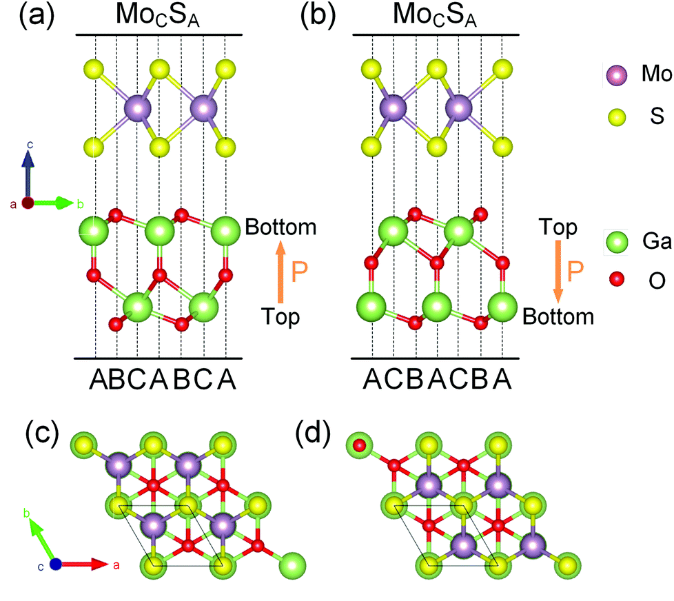 | ||
| Fig. 1 The most stable stacking structures of bilayers: (a and c) MoS2/Ga2O3↑ and (b and d) MoS2/Ga2O3↓. The Mo, S, Ga and O atoms are colored in purple, yellow, green, red, respectively. The directions of dipole moment are indicated by the orange arrows in (a) and (b). The black parallelograms indicate the primitive cells in (c) and (d). | ||
We consider all six possible high-symmetric stacking structures for each dipole model (twelve in total) as we have done in the previous report,42,43 and the corresponding models are shown in Fig. S1 and S2.† We define the stacking sites of the Ga2O3 layer as (1) site A – central O and bottom Ga atoms; (2) site B – top and bottom O atoms; and (3) site C – top Ga atom. In this way, the stacking structures of the upper MoS2 layer are labeled with the subscript stacking sites as, for example, MoCSA. Among all the high-symmetric stacking structures, MoS2/Ga2O3↑–MoCSA and MoS2/Ga2O3↓–MoCSA are the most stable ones, as shown in Fig. 1. Interestingly, both dipole models have the same vertical stacking arrangements: the hollow site of MoS2 faces the site B of Ga2O3; the S atom faces the site A; and the Mo atoms faces the site C. The results show that all the stacking configurations with the upper S atoms right above the lower O atoms are not stable since the same charged centers get relatively close to each other. The other configurations have relatively small energy differences of less than 7 meV per unit cell, as shown in Tables S1 and S2.† We use MoS2/Ga2O3↑ and MoS2/Ga2O3↓ herein to refer to the two most stable structures, respectively.
The optimized interlayer distances of the MoS2/Ga2O3↑ and MoS2/Ga2O3↓ are 2.73 and 2.72 Å (vertical distances between the facing O and S atoms), respectively, and the binding energies (Ebinding) are −42.02 and −44.05 meV Å−2, respectively. The negative binding energies demonstrate the energetic stabilities of the MoS2/Ga2O3 heterostructures. We note that the binding energies in this work are larger than the vdW binding energy range of ∼−20 meV Å−2 suggested in Refs. 44, 45, because the hybrid functional and vdW correction adopted here (see Computational details) are different. Nevertheless, the interlayer interaction is predominant by vdW interaction, because the long interlayer distances and only marginal charge transfers (less than 0.01 e per unit cell) identified by Bader charge analysis46 are both typical for a vdW interaction. Moreover, the further detailed analyses on the electronic structures can provide useful information as well.
An ab initio molecular dynamics (AIMD) simulations at 300 K were conducted for (3 × 3) supercells to verify the thermostability of MoS2/Ga2O3 heterostructures under relaxed station and 6% tensile strain.47 As shown in Fig. S3,† the temperature and total energy of systems during AIMD simulations fluctuate with small ups and downs, indicating the excellent thermostability. After 5 ps AIMD calculations at 300 K, the atoms only have tiny displacements from their original equilibrium positions and no structural corruption are observed. After going through an extra structural relaxation, the distorted structure can basically return to its original well-symmetrical structure. Hence, the excellent thermostability is confirmed for MoS2/Ga2O3 heterostructures.
3.2 Electronic properties
The HSE06 band gaps of the relaxed MoS2 and FE-ZB’ Ga2O3 monolayers are 2.35 and 3.19 eV, respectively, consistent with the previous calculations.26,45 The in-plane lattice constants (3.06 Å) of the bilayers lead to compressive strain on MoS2 layer, while tensile strain on Ga2O3 layer. Generally, it is expected that this initial strain further results in an opposite effect on the individual band gaps of the monolayers. Therefore, the band gap of MoS2 in the bilayer system is larger than that of the relaxed monolayer,32 while the counterpart of Ga2O3 will be smaller.26As shown in Fig. 2a, MoS2/Ga2O3↑ has a direct band gap of 2.63 eV. The valence band maximum (VBM) and conduction band minimum (CBM) are located at the high-symmetric K point. MoS2 layer contributes the most to the valence band region near VBM and the conduction band region near CBM, as indicated by the red-colored bands in Fig. 2a. So MoS2/Ga2O3↑ belongs to the straddling type-I semiconductor heterostructure with very small VB and CB offsets of 0.13 and 0.37 eV, respectively.
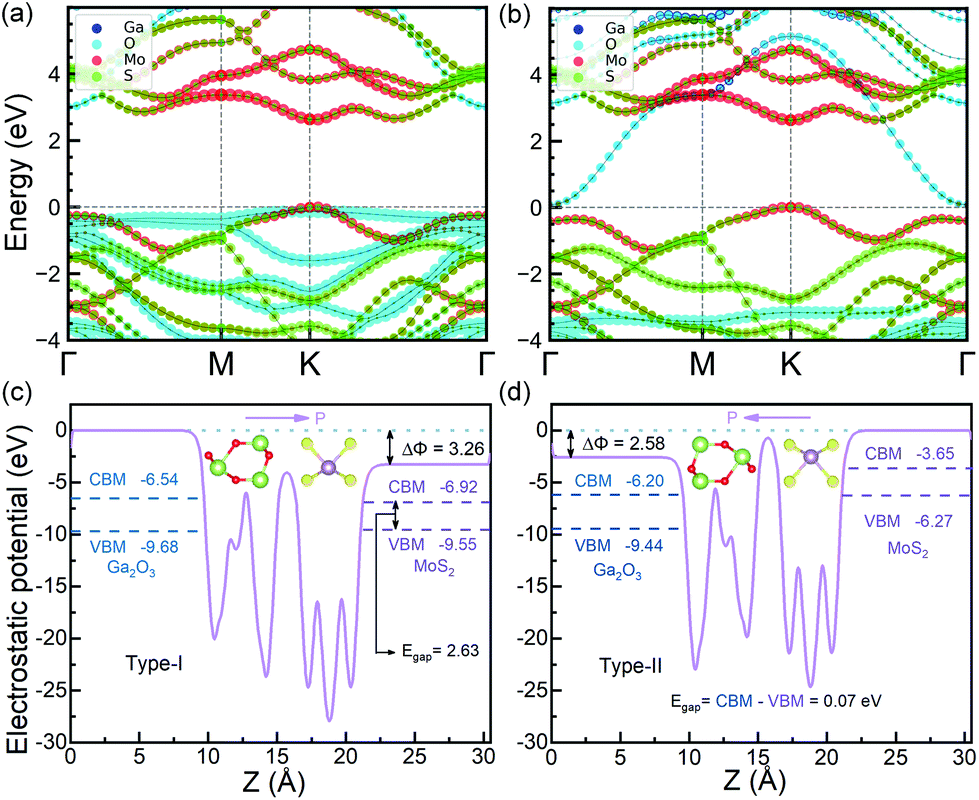 | ||
| Fig. 2 Band structure of (a) MoS2/Ga2O3↑ and (b) MoS2/Ga2O3↓ heterostructures. The VBMs are leveled to zero eV. Averaged electrostatic potential of (c) MoS2/Ga2O3↑ and (d) MoS2/Ga2O3↓ along the z-direction. In (a and b), the contribution strength from Ga, O, Mo and S orbitals are colored in blue, cyan, red and green, respectively. | ||
The detailed analysis of the projected band structure reveals that VBM (K) is mainly composed of in-plane Mo-4dxy/dx2–y2 and small fractions of S-3px/py orbits, while CBM (K) is largely composed of Mo-4dz2/5s and only trace amount of S-3py/px orbits. The detailed orbital occupancy diagram is shown in Fig. S4.† The average electrostatic potential curve of MoS2/Ga2O3↑ along the z-axis is shown in Fig. 2c. The vacuum potential difference between the upper and lower surfaces of the bilayer systems (the offset in the electrostatic potential curve, the ΔΦ of MoS2/Ga2O3↑ is 3.26 eV). Compared to the Ga2O3 and In2Se3 monolayer, the ΔΦ of MoS2/Ga2O3↑ is slightly lower than that of Ga2O3 monolayer (3.47 eV),26 but still much higher than that of In2Se3 monolayer (1.37 eV).20
As shown in Fig. 2b, MoS2/Ga2O3↓ has an indirect band gap of 0.07 eV, showing a heavily staggered type-II heterostructure feature. The VBM is located at the high-symmetric K point contributed by MoS2, and CBM is located at Γ point contributed by Ga2O3. Therefore, MoS2/Ga2O3↓ heterostructure has the band edges spatially separated by the vdW interlayer gap. Unlike the MoS2/Ga2O3↑ bilayer, the CBM (Γ) is composed of Ga-4s/4pz and O-2s/2pz orbitals. The detailed orbital occupancy diagram is shown in Fig. S5.† The electrostatic potential curve of MoS2/Ga2O3↓ along the z-axis is shown in Fig. 2d, where the ΔΦ of MoS2/Ga2O3↓ is 2.58 eV.
The band gap of MoS2/Ga2O3↑ and MoS2/Ga2O3↓ have a significant difference attributed to the ferroelectric nature of the FE-ZB’ Ga2O3, which is consistent with the previous observation in WSe2/In2Se3 heterojunction.20 Similarly, WSe2 and MoS2 belong to paraelectric TMDCs, while both the FE-ZB’ In2Se3 and Ga2O3 have ferroelectric properties. Comparing Fig. 2a and b, the energy band of MoS2 is pulled up by ∼3 eV relative to Ga2O3 in MoS2/Ga2O3↓ due to the change of spontaneous dipole direction. Since the dipole direction of the heterostructure can lead to the significant difference of the band gaps, a simple switch model can be constructed by applying an out-of-plane electric field, which will be discussed in the last section.
3.3 Carrier mobility
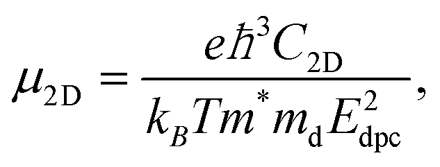
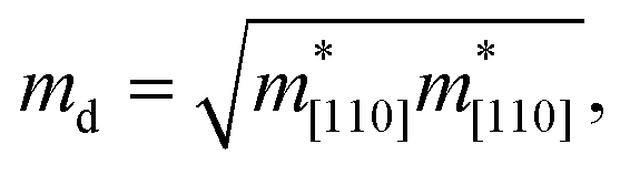
The carrier mobility not only affects the photocatalytic efficiency but also plays as one of the most important parameters for determining the performance of electronic devices.14,48,49 The calculated electron and hole effective masses of MoS2/Ga2O3↑ are 0.43 and −5.52 m0 (m0 is the free-electron mass), respectively, along the [110] direction of the hexagonal cell. The hole effective mass is a factor of ∼13 times larger than that of electron. It can also be seen from the band structure in Fig. 2a where the curvature of VBM is much flatter than the CBM counterpart.Based on the deformation potential theory, the electron mobility of 2D Ga2O3 and MoS2 heterostructure was calculated by:26,50
 | (1) |
 | (2) |
 | (3) |
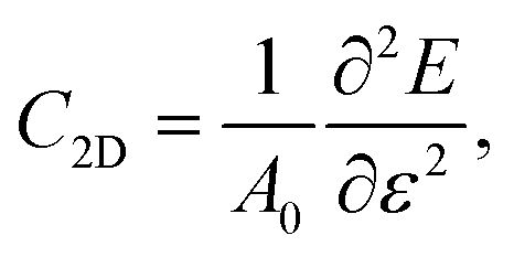
| Edpc = ΔECBM/ε, | (4) |
The directions of [10] and [110] in the real space correspond to Γ–M and Γ–K in the reciprocal space, respectively. As indicated by the calculated data in Table 1, the electron mobilities of MoS2/Ga2O3↑ are about 1.5 times of the ones of MoS2/Ga2O3↓. This is because the lowest conduction band in [10] and [110] direction of MoS2/Ga2O3↓ is mainly located on the Ga2O3 layer, while MoS2/Ga2O3↑ is mainly located on the MoS2 layer, as shown in Fig. 2, which leads to different effective mass and deformation potential constant. Even though, the electron mobility is close to 2000 cm2 V−1 s−1, which obviously exceeds MoS2 monolayer (∼ 200 cm2 V−1 s−1).51
10] and [110] directions. Note that all calculations used the HSE06 hybrid functional.38
| Materials | m* (m0) | E dpc (eV) | C 2D (J m−2) | μ 2D (cm2 V−1 s−1) |
|---|---|---|---|---|
| MoS2/Ga2O3↑ [10] |
0.428 | −3.198 | 284.785 | 3254 |
| MoS2/Ga2O3↑ [110] | 0.426 | −3.194 | 270.055 | 3107 |
| MoS2/Ga2O3↓ [10] |
0.417 | −4.471 | 283.141 | 1761 |
| MoS2/Ga2O3↓ [110] | 0.407 | −4.171 | 268.372 | 1965 |
In order to better observe the influence of CBM in different layers on the electron mobility, the real-space probability distribution at CBM of these two heterostructures are shown in Fig. S6.† Overlapping wave functions and bonding characteristics of MoS2/Ga2O3↑ are stronger than MoS2/Ga2O3↓, which corresponds to the higher electron mobility.
3.4 Biaxial strain engineering
In 2D materials, energy band structure, electrical and optical properties can be tuned by applying in-plane strain.43,52,53 This strain effect has a guiding significance for exploring novel physics in 2D materials and the applications of flexible devices.54 In this section, we focus on the tunable structural and electronic properties of the MoS2/Ga2O3 bilayers via biaxial strain engineering.The band structures of MoS2/Ga2O3↑ under biaxial strains ranging from −6% to 6% are shown in Fig. 3. Not only the transition from the type-I to type-II heterostructure but also the indirect-direct transition of the band gap are observed. From the compressively strained to non-strained state, the CBM changes from the k-point in between K and Γ to the high-symmetry K point as shown in Fig. 2a and 3c. Within the calculated strain range, we note that the CBM is always contributed by the MoS2 layer. The VBM is always located at the high-symmetry K point. In the tensile strains range from 0% to 6%, the VBM shifts from MoS2 to Ga2O3, which further leads to the type-I → type-II transition of the bilayer heterostructure.
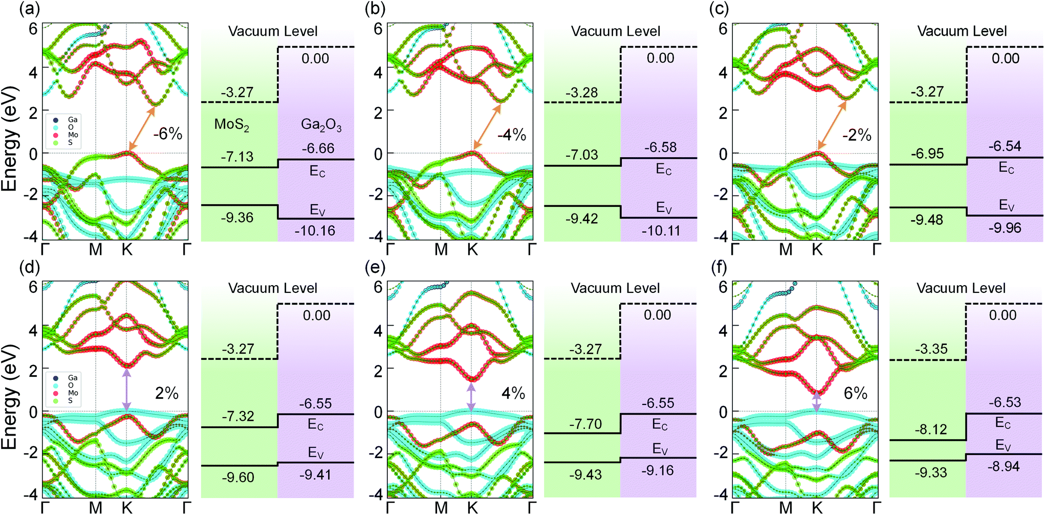 | ||
| Fig. 3 Band structures (left panels) and band alignment diagrams (right panels) of MoS2/Ga2O3↑ heterostructure with biaxial strains of (a) −6%, (b) −4%, (c) −2%, (e) 2%, (f) 4%, and (g) 6%. In (a–f), the orange and purple arrows indicate the indirect and direct band gap, respectively. | ||
In contrast, the band structures of MoS2/Ga2O3↓ under biaxial strain reveal a type-II → type-III transition, as shown in Fig. 4. From compressive to tensile strain, the shape of the VB edge contributed by the MoS2 layer changes significantly. The Γ-point VB edge rises against the K-point VB edge and becomes the VBM at the biaxial strain of 2%. Meanwhile, the VBM (Γ) overlaps with the CBM (Γ) from the Ga2O3 layer.
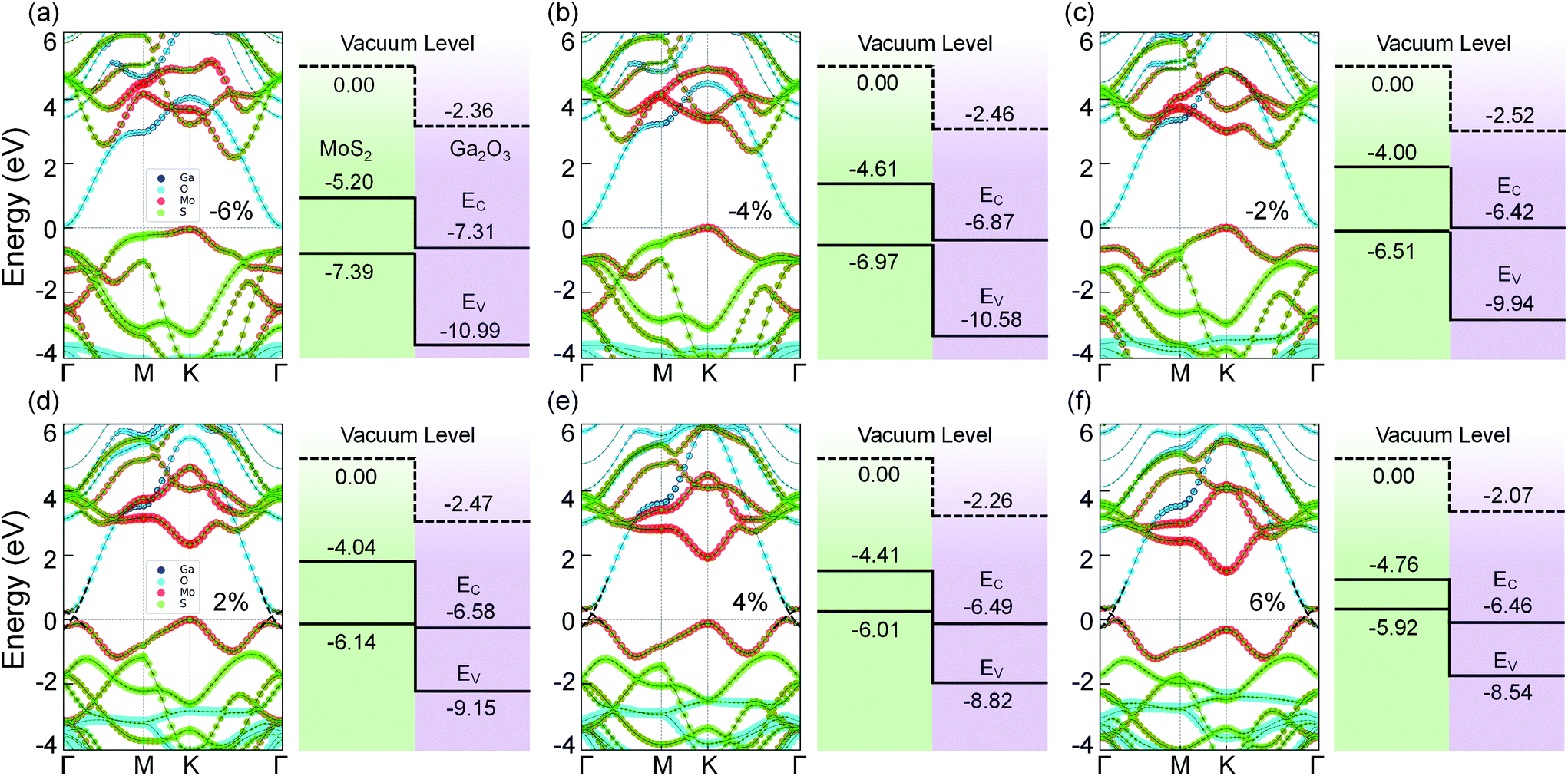 | ||
| Fig. 4 Band structures (left panels) and band alignment diagrams (right panels) of MoS2/Ga2O3↓ heterostructure with biaxial strains of (a) −6%, (b) −4%, (c) −2%, (d) 2%, (e) 4%, and (f) 6%. In (d–f), the black dashed lines indicate the VBM and CBM bands are crossing each other near Γ point. | ||
As shown in Fig. 5a, with the biaxial strains changing from −6% to no strain case, the band gap of MoS2/Ga2O3↑ increases first, reaching the maximum value of 2.57 eV at 0%. Since both CBM and VBM are contributed by the MoS2 layer (see Fig. 3), the tendency here is expected to be very similar to the results of the MoS2 monolayer under compressive strain.55 The difference is seen in the tensile strains ranging from 2% to 6%, as the VBM is replaced by the Ga2O3 layer. Overall, the band gap remains to be direct and linearly decrease to 0.8 eV at 6%. On the contrast, the overall band gap of MoS2/Ga2O3↓ model changes very little under compressive strain. From 2% to 6%, the band gap breaks at the Γ point where the VBM of the MoS2 is above the CBM of the Ga2O3.
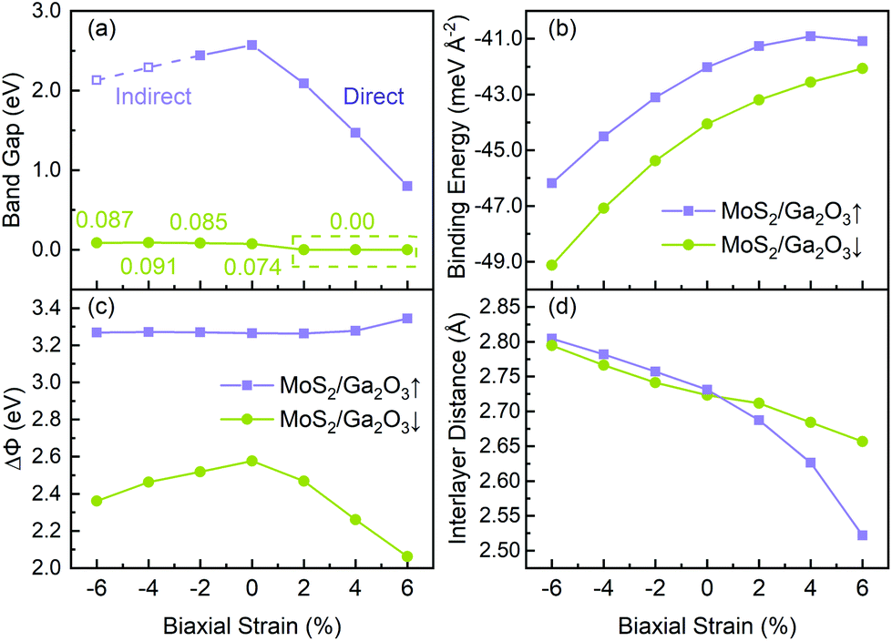 | ||
| Fig. 5 (a) Band gap, (b) binding energy, (c) ΔΦ and (d) interlayer distance of MoS2/Ga2O3↑ and MoS2/Ga2O3↓ versus biaxial strains, respectively. In (a), the dashed line and hollow square show the indirect band gap in the corresponding strain range, while the solid line and square indicate the direct band gap. | ||
Fig. 5c shows the correlation between the vacuum level difference (ΔΦ) and the biaxial strain. The ΔΦ of MoS2/Ga2O3↑ remains almost unchanged, which is similar to the result of Ga2O3 monolayer.26 However, the ΔΦ of MoS2/Ga2O3↓ changes much more sensitively with the biaxial strain. Moreover, the nonmonotonic relation is seen here: the ΔΦ of MoS2/Ga2O3↓ increases from 2.37 eV to the maximum value of 2.58 eV in the range of −6% to 0%, and decreases to the minimum value of 2.07 eV at 6%.
The binding energy of MoS2/Ga2O3 heterostructure is calculated by:56,57
 | (5) |
 represents the total energies of the MoS2/Ga2O3 heterostructure,
  and
and  are the energies of Ga2O3 and MoS2 monolayer relaxed under certain biaxial strain, respectively, and S is the in-plane area of the unit cells. As shown in Fig. 5b, the binding energies fall into approximated quadratic-inverse curves, because the in-plane area S increases as a quadratic function of biaxial strain, while the vdW interaction strength remains almost unchanged to biaxial strain. The results also validate the vdW nature of the interlayer interaction as discussed in section 1. The interlayer distance of MoS2/Ga2O3↑ and MoS2/Ga2O3↓ both show a decreasing trend as expected, shown in Fig. 5d.
3.5 Optical properties
In order to further study the photon absorption capacity of MoS2/Ga2O3 bilayers, we calculated their absorption spectra under different strains. The absorption coefficient α(E) can be obtained by:43 | (6) |
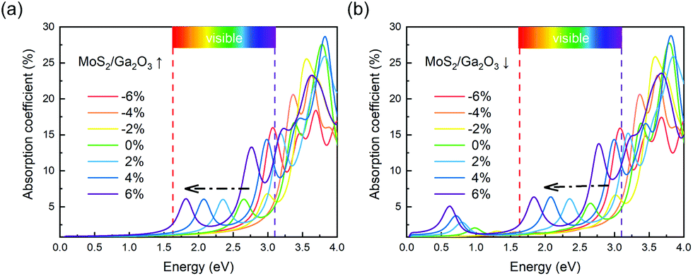 | ||
| Fig. 6 Optical absorption spectra of (a) MoS2/Ga2O3↑ and (b) MoS2/Ga2O3↓ heterostructures. The visible-light range is labeled from 1.63 to 3.1 eV in (a) and (b). | ||
3.6 Photocatalytic and electrical applications
So far, we have systematically studied the structural, electronic and optical properties of the two stable configurations of the ferroelectric MoS2/Ga2O3 heterobilayers. Several unique and desired features, such as small interlayer lattice mismatch, large electron mobility, highly tunable band alignment and optical absorption, can lead to promising utility of the heterobilayers in the field of photocatalytic and electronic devices. More essentially, the intrinsic ferroelectrics will add new possibility of enhanced performance and controllability, which we will discuss in detail in this section.As shown in Fig. 7a, in the MoS2/Ga2O3↓ system, the real-space probability distributions (squared wavefunction) of VBM (K) and CBM (Γ) locate on the different layers. In opposite, the VBM (K) and CBM (K) of the MoS2/Ga2O3↑ are both located on MoS2 layer (Fig. S8†). This result is in good accordance with the analyses of the band structure (Fig. 2). This long-distance spatial separation between the VBM and CBM can result in long-lifetime electron–hole pair which is favorable for further water-splitting reaction.42
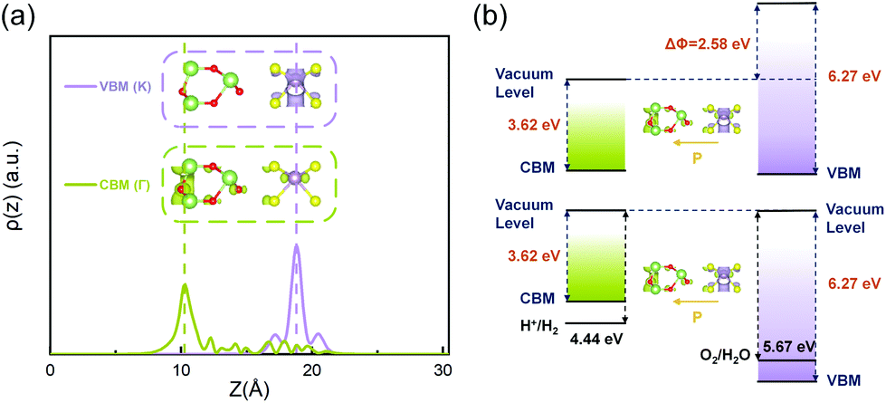 | ||
| Fig. 7 (a) The real-space probability distribution of VBM and CBM bands of the MoS2/Ga2O3↓ heterostructure along the z-direction. (b) Band alignment of the MoS2/Ga2O3↓ heterostructure with different vacuum levels (upper panel) and aligned vacuum levels (lower panel). In (a), the insets show its real-space probability distribution of CBM (Γ) and VBM (K), respectively, with the same isosurface level at 2.57 × 10⁻⁸ e per Bohr3. In (b), the black solid lines represent the water redox potentials at −4.44 eV and −5.67 eV.42 | ||
Additionally, the energy band gap of the MoS2/Ga2O3↓ is too small for the minimum chemical potential difference (∼1.3 eV) between Hydrogen Evolution Reaction (HER) and Oxygen Evolution Reaction (OER). However, with the intrinsic polarization, the vacuum potential difference, ΔΦ, between upper and lower surfaces is as large as 2.58 eV, as indicated in the band diagram (upper panel of Fig. 7b). When photons are adsorbed by MoS2/Ga2O3↓ to generate electron–hole pairs, excited electrons will be further accelerated when transferring to the CB on the bottom surface of Ga2O3 because of the built-in polarization. Hence, smaller photon energy is required to excite electron–hole pairs, therefore greatly enhancing the use of photon energy in the infrared region. Therefore, ΔΦ can act as an auxiliary booster for photoexcited electrons and effectively reduce the photocatalyst's band gap required for water splitting.62,63
We further illustrate this boosting effect by aligning the vacuum levels, as shown in the lower panel of Fig. 7b. In this way, the origin of the energy difference between effective CBM and VBM of MoS2/Ga2O3↓ consists of band gap energy and ΔΦ. As clearly shown, the effective CBM of MoS2/Ga2O3↓ is higher than the reduction level of hydrogen ion (−4.44 eV, under pH = 0) and the effective VBM is lower than the oxidation level of oxygen (−5.67 eV, under pH = 0), satisfying the required conditions of water splitting. The relationship between water reduction-oxidation (Redox) potential and pH value can be further determined by:64,65
| EH+/H2 = −4.44 eV + pH × 0.059 eV, | (7) |
| EO2/H2O = −5.67 eV + pH × 0.059 eV. | (8) |
Therefore, MoS2/Ga2O3↓ bilayer system meets the water redox potential difference with an excellent pH tolerance ranging from pH = 0 to pH = 13.2 and even more acidic environment.
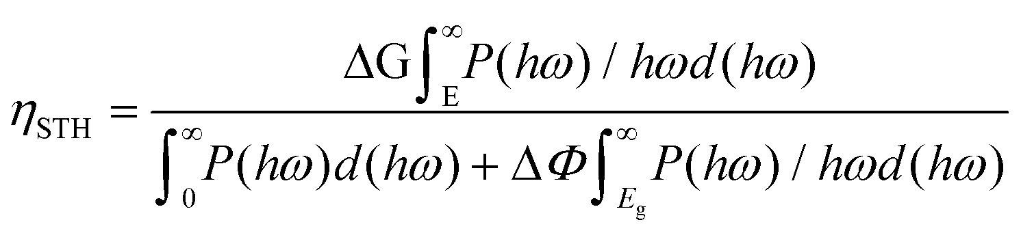
Since photogenerated electrons and holes are distributed separately in Ga2O3 and MoS2, as a result, the recombination process is suppressed. Compared with other photocatalytic water-splitting materials,45,66 MoS2/Ga2O3↓ system has stronger optical harvesting in the infrared region, more efficient charge separation, and faster transportation/mobility of both electron and hole to reach higher solar-to-hydrogen (STH) efficiencies. In order to meet the requirements of practical application, the STH efficiency of photocatalysts is required to be at least above 10%.67 The STH efficiency of photocatalytic water splitting for 2D material with vertical intrinsic ferroelectrics is calculated as68
 | (9) |
Moreover, to readily control the “ON” and “OFF” states of the reaction, we will demonstrate a switching mechanism based on the polarization reversal transition of the Ga2O3 layer via external electric field.
As shown in Fig. 8a, with different electric fields along the z-axis ranging from −4.0 to 8.0 V nm−1 (positive value pointing downwards) with 1.0 V nm−1 in step, the energy difference between the MoS2/Ga2O3↑ and MoS2/Ga2O3↓ configurations, ΔE, changes linearly with the electric field. The vertical dashed lines shown in Fig. 8a represent the positions of the highest points of the two curves, the corresponding electric fields are also consistent with the electrostatic potential differences (ΔΦ in Fig. 2c and d). The calculations show that an electric field of 8 V nm−1 will result in an energy difference of up to 0.272 eV per unit cell. According to Boltzmann distribution, the ratio of two phase populations at equilibrium can be estimated by:
 | (10) |
![[thin space (1/6-em)]](https://www.rsc.org/images/entities/char_2009.gif) 000 at 300 K. Therefore, we further propose a switching device model as illustrated in Fig. 8b. By applying bias at the gate (G), the FE-ZB’ Ga2O3 monolayer goes through the polarization reversal transition to the energetically favorable state, for example, from MoS2/Ga2O3↑ to MoS2/Ga2O3↓. Meanwhile, the band alignment of the heterobilayer changes from straddling type-I to heavily staggered type-II (see Fig. 2), and also the photocatalytic and electrical properties are distinctly switched. Finally, it is worth noting that this switching mechanism can be further coupled with in-plane strain engineering to achieve more precise tunablity.
000 at 300 K. Therefore, we further propose a switching device model as illustrated in Fig. 8b. By applying bias at the gate (G), the FE-ZB’ Ga2O3 monolayer goes through the polarization reversal transition to the energetically favorable state, for example, from MoS2/Ga2O3↑ to MoS2/Ga2O3↓. Meanwhile, the band alignment of the heterobilayer changes from straddling type-I to heavily staggered type-II (see Fig. 2), and also the photocatalytic and electrical properties are distinctly switched. Finally, it is worth noting that this switching mechanism can be further coupled with in-plane strain engineering to achieve more precise tunablity.
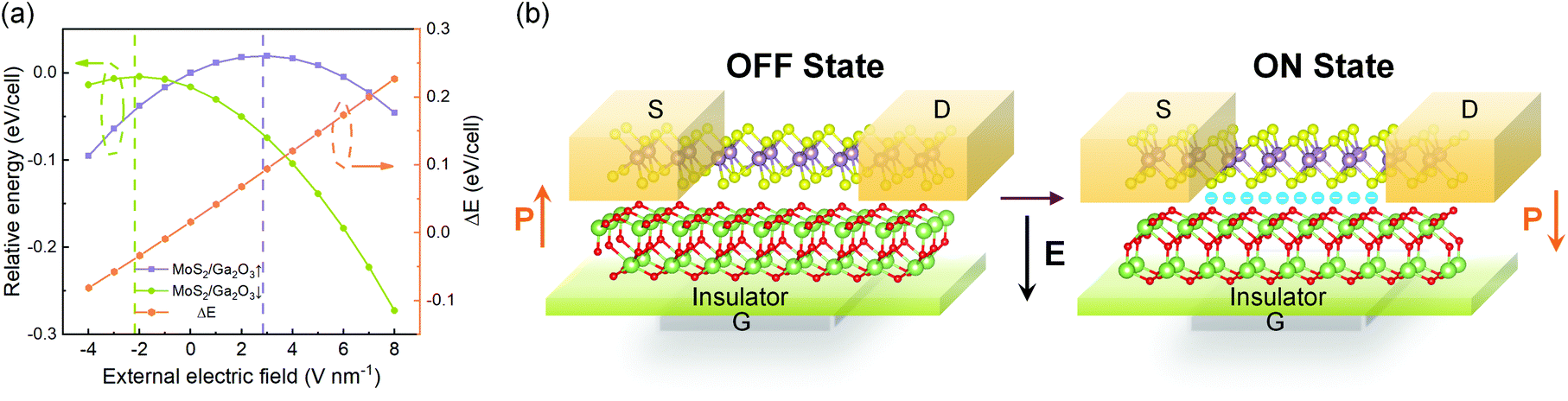 | ||
| Fig. 8 (a) The calculated energy difference under vertical external electric fields. The energy of relaxed MoS2/Ga2O3↑ is set to be 0 eV for the left axis. ΔE of the right axis is the energy difference between MoS2/Ga2O3↑ and MoS2/Ga2O3↓ under the same electric field. The vertical lines represent the positions of the highest points of the two curves, respectively. (b) A switching device model under an applied electric field. The black arrow indicates the applied electric field. The cyan circles indicate the electrons under “ON” state. | ||
4 Conclusions
In summary, we have systematically studied the electrical and optical properties of the 2D vdW MoS2/Ga2O3 heterostructures with two dipole models through first-principles calculations. MoS2/Ga2O3↑and MoS2/Ga2O3↓ exhibit different types of band alignment (straddling type-I and staggered type-II) at their relaxed states. The heterostructure types of MoS2/Ga2O3 can be precisely engineered in a moderate range of biaxial strain. By applying strain to MoS2/Ga2O3, it still has a suitable band gap and excellent optical absorption capacity ranging from visible light to ultraviolet light, ensuring promising applications in flexible electrical and optical devices. For MoS2/Ga2O3↓ heterostructure (type-II), larger spatial separation of the valence and conduction band edges and excellent optical absorption ranging from infrared to ultraviolet region under biaxial strain are favorable for water-splitting reaction. With the assistance of a modest electric field, there is a distinct state transition between MoS2/Ga2O3↑ and MoS2/Ga2O3↓, guaranteeing the practical usage of such heterogeneous bilayers with intrinsic ferroelectrics.Conflicts of interest
The authors declare no competing financial interest.Acknowledgements
This work was supported by the High-Level University Fund (G02236002 and G02236005) at Southern University of Science and Technology. This computational work was supported by the Center for Computational Science and Engineering at Southern University of Science and Technology. The authors thank Yikai Liao at National University of Singapore for a useful discussion on carrier mobility.References
- K. S. Novoselov, A. K. Geim, S. V. Morozov, D. Jiang, Y. Zhang, S. V. Dubonos, I. V. Grigorieva and A. A. Firsov, Science, 2004, 306, 666–669 CrossRef CAS PubMed.
- K. Watanabe, T. Taniguchi and H. Kanda, Nat. Mater., 2004, 3, 404–409 CrossRef CAS PubMed.
- K. F. Mak, C. Lee, J. Hone, J. Shan and T. F. Heinz, Phys. Rev. Lett., 2010, 105, 136805 CrossRef PubMed.
- Q. H. Wang, K. Kalantar-Zadeh, A. Kis, J. N. Coleman and M. S. Strano, Nat. Nanotechnol., 2012, 7, 699–712 CrossRef CAS PubMed.
- A. Zavabeti, J. Z. Ou, B. J. Carey, N. Syed, R. Orrell-Trigg, E. L. H. Mayes, C. Xu, O. Kavehei, A. P. O'Mullane, R. B. Kaner, K. Kalantar-zadeh and T. Daeneke, Science, 2017, 358, 332–335 CrossRef CAS PubMed.
- B. Y. Zhang, K. Xu, Q. F. Yao, A. Jannat, G. H. Ren, M. R. Field, X. M. Wen, C. H. Zhou, A. Zavabeti and J. Z. Ou, Nat. Mater., 2021, 20, 1073–1078 CrossRef CAS PubMed.
- A. K. Geim and I. V. Grigorieva, Nature, 2013, 499, 419–425 CrossRef CAS PubMed.
- Y. Cao, V. Fatemi, S. Fang, K. Watanabe, T. Taniguchi, E. Kaxiras and P. Jarillo-Herrero, Nature, 2018, 556, 43–50 CrossRef CAS PubMed.
- B. Jäck, Y. Xie and A. Yazdani, Nat. Rev. Phys., 2021, 3, 541–554 CrossRef.
- D. Deng, K. S. Novoselov, Q. Fu, N. Zheng, Z. Tian and X. Bao, Nat. Nanotechnol., 2016, 11, 218–230 CrossRef CAS PubMed.
- Y. Chen, Y. Wang, Z. Wang, Y. Gu, Y. Ye, X. Chai, J. Ye, Y. Chen, R. Xie, Y. Zhou, Z. Hu, Q. Li, L. Zhang, F. Wang, P. Wang, J. Miao, J. Wang, X. Chen, W. Lu, P. Zhou and W. Hu, Nat. Electron., 2021, 4, 357–363 CrossRef CAS.
- H. Chen, X. Xue, C. Liu, J. Fang, Z. Wang, J. Wang, D. W. Zhang, W. Hu and P. Zhou, Nat. Electron., 2021, 4, 399–404 CrossRef CAS.
- K. S. Novoselov, A. Mishchenko, A. Carvalho and A. H. Castro Neto, Science, 2016, 353, aac9439 CrossRef CAS PubMed.
- C. Song, G. Noh, T. S. Kim, M. Kang, H. Song, A. Ham, M.-k. Jo, S. Cho, H.-J. Chai and S. R. Cho, et al. , ACS Nano, 2020, 14, 16266–16300 CrossRef CAS PubMed.
- H. Yang, J. Heo, S. Park, H. J. Song, D. H. Seo, K.-E. Byun, P. Kim, I. Yoo, H.-J. Chung and K. Kim, Science, 2012, 336, 1140–1143 CrossRef CAS PubMed.
- L. Britnell, R. M. Ribeiro, A. Eckmann, R. Jalil, B. D. Belle, A. Mishchenko, Y.-J. Kim, R. V. Gorbachev, T. Georgiou, S. V. Morozov, A. N. Grigorenko, A. K. Geim, C. Casiraghi, A. H. C. Neto and K. S. Novoselov, Science, 2013, 340, 1311–1314 CrossRef CAS PubMed.
- A. N. Grigorenko, M. Polini and K. S. Novoselov, Nat. Photonics, 2012, 6, 749–758 CrossRef CAS.
- M. Dawber, K. M. Rabe and J. F. Scott, Rev. Mod. Phys., 2005, 77, 1083–1130 CrossRef CAS.
- C. Noguera, J. Phys.: Condens. Matter, 2000, 12, R367–R410 CrossRef CAS.
- W. Ding, J. Zhu, Z. Wang, Y. Gao, D. Xiao, Y. Gu, Z. Zhang and W. Zhu, Nat. Commun., 2017, 8, 14956–14956 CrossRef CAS PubMed.
- Y. Zhou, D. Wu, Y. Zhu, Y. Cho, Q. He, X. Yang, K. Herrera, Z. Chu, Y. Han, M. C. Downer, H. Peng and K. Lai, Nano Lett., 2017, 17, 5508–5513 CrossRef CAS PubMed.
- R. Mankowsky, A. von Hoegen, M. Först and A. Cavalleri, Phys. Rev. Lett., 2017, 118, 197601 CrossRef CAS PubMed.
- L. Qi, S. Ruan and Y.-J. Zeng, Adv. Mater., 2021, 33, 2005098 CrossRef CAS PubMed.
- Z. Guan, H. Hu, X. Shen, P. Xiang, N. Zhong, J. Chu and C. Duan, Adv. Electron. Mater., 2020, 6, 1900818 CrossRef CAS.
- M. Wu and P. Jena, Wiley Interdiscip. Rev.: Comput. Mol. Sci., 2018, 8, e1365 Search PubMed.
- Y. Liao, Z. Zhang, Z. Gao, Q. Qian and M. Hua, ACS Appl. Mater. Interfaces, 2020, 12, 30659–30669 CrossRef CAS PubMed.
- J. Zhao, J. Byggmästar, Z. Zhang, F. Djurabekova, K. Nordlund and M. Hua, Phys. Rev. B, 2021, 104, 054107 CrossRef CAS.
- J. Zhao, X. Huang, Y. Yin, Y. Liao, H. Mo, Q. Qian, Y. Guo, X. Chen, Z. Zhang and M. Hua, J. Phys. Chem. Lett., 2021, 12, 5813–5820 CrossRef CAS PubMed.
- G. Liu, Z. Zhang, H. Wang, G.-L. Li, J.-S. Wang and Z. Gao, J. Appl. Phys., 2021, 130, 105106 CrossRef CAS.
- X. Duan, C. Wang, A. Pan, R. Yu and X. Duan, Chem. Soc. Rev., 2015, 44, 8859–8876 RSC.
- Q. Qian, J. Lei, J. Wei, Z. Zhang, G. Tang, K. Zhong, Z. Zheng and K. J. Chen, npj 2D Mater. Appl., 2019, 3, 1–9 CrossRef CAS.
- R. Ganatra and Q. Zhang, ACS Nano, 2014, 8, 4074–4099 CrossRef CAS PubMed.
- Q. Qian, Z. Zhang and K. J. Chen, Phys. Rev. B, 2018, 97, 165409 CrossRef CAS.
- J. Li, X. Zhang, B. Yang, C. Zhang, T. Xu, L. Chen, L. Yang, X. Jin and B. Liu, Chem. Mater., 2021, 33, 4568–4577 CrossRef CAS.
- G. Kresse and J. Furthmüller, Comput. Mater. Sci., 1996, 6, 15–50 CrossRef CAS.
- P. E. Blöchl, Phys. Rev. B: Condens. Matter Mater. Phys., 1994, 50, 17953–17979 CrossRef PubMed.
- J. Heyd, G. E. Scuseria and M. Ernzerhof, J. Chem. Phys., 2006, 124, 219906 CrossRef.
- J. Paier, M. Marsman, K. Hummer, G. Kresse, I. C. Gerber and J. G. Ángyán, J. Chem. Phys., 2006, 125, 249901 CrossRef.
- S. Grimme, J. Antony, S. Ehrlich and H. Krieg, J. Chem. Phys., 2010, 132, 154104 CrossRef PubMed.
- V. Wang, N. Xu, J.-C. Liu, G. Tang and W.-T. Geng, Comput. Phys. Commun., 2021, 267, 108033 CrossRef CAS.
- K. Momma and F. Izumi, J. Appl. Crystallogr., 2011, 44, 1272–1276 CrossRef CAS.
- Z. Zhang, Q. Qian, B. Li and K. J. Chen, ACS Appl. Mater. Interfaces, 2018, 10, 17419–17426 CrossRef CAS PubMed.
- Z. Zhang, B. Huang, Q. Qian, Z. Gao, X. Tang and B. Li, APL Mater., 2020, 8, 041114 CrossRef CAS.
- T. Björkman, A. Gulans, A. V. Krasheninnikov and R. M. Nieminen, Phys. Rev. Lett., 2012, 108, 235502 CrossRef PubMed.
- H. Guo, Z. Zhang, B. Huang, X. Wang, H. Niu, Y. Guo, B. Li, R. Zheng and H. Wu, Nanoscale, 2020, 12, 20025–20032 RSC.
- M. Yu and D. R. Trinkle, J. Chem. Phys., 2011, 134, 064111 CrossRef PubMed.
- J.-J. Zhang, J. Guan, S. Dong and B. I. Yakobson, J. Am. Chem. Soc., 2019, 141, 15040–15045 CrossRef CAS PubMed.
- D. S. Schulman, A. J. Arnold and S. Das, Chem. Soc. Rev., 2018, 47, 3037–3058 RSC.
- Y. Zhang, S.-M. Zhao, Q.-W. Su and J.-L. Xu, Rare Met., 2021, 40, 96–104 CrossRef.
- J. Qiao, X. Kong, Z.-X. Hu, F. Yang and W. Ji, Nat. Commun., 2014, 5, 1–7 Search PubMed.
- Y. Cai, G. Zhang and Y.-W. Zhang, J. Am. Chem. Soc., 2014, 136, 6269–6275 CrossRef CAS PubMed.
- S.-K. Lee, B. J. Kim, H. Jang, S. C. Yoon, C. Lee, B. H. Hong, J. A. Rogers, J. H. Cho and J.-H. Ahn, Nano Lett., 2011, 11, 4642–4646 CrossRef CAS PubMed.
- X. Liu, Z. Zhang, Z. Luo, B. Lv and Z. Ding, Nanomaterials, 2019, 9, 1674 CrossRef CAS PubMed.
- W. S. Yun, S. W. Han, S. C. Hong, I. G. Kim and J. D. Lee, Phys. Rev. B: Condens. Matter Mater. Phys., 2012, 85, 033305 CrossRef.
- P. Lu, X. Wu, W. Guo and X. C. Zeng, Phys. Chem. Chem. Phys., 2012, 14, 13035–13040 RSC.
- J. Liao, B. Sa, J. Zhou, R. Ahuja and Z. Sun, J. Phys. Chem. C, 2014, 118, 17594–17599 CrossRef CAS.
- H. Guo, Z. Zhang, Y. Guo, Z. Gao, R. Zheng and H. Wu, Appl. Surf. Sci., 2020, 505, 144650 CrossRef CAS.
- W. Meng, X. Wang, Z. Xiao, J. Wang, D. B. Mitzi and Y. Yan, J. Phys. Chem. Lett., 2017, 8, 2999–3007 CrossRef CAS PubMed.
- S. Chen, T. Takata and K. Domen, Nat. Rev. Mater., 2017, 2, 1–17 CrossRef.
- T. Takata, J. Jiang, Y. Sakata, M. Nakabayashi, N. Shibata, V. Nandal, K. Seki, T. Hisatomi and K. Domen, Nature, 2020, 581, 411–414 CrossRef CAS PubMed.
- T. J. Mills, F. Lin and S. W. Boettcher, Phys. Rev. Lett., 2014, 112, 148304 CrossRef PubMed.
- B. Zhou, K. Jiang, L. Shang, J. Zhang, Y. Li, L. Zhu, S.-J. Gong, Z. Hu and J. Chu, J. Mater. Chem. C, 2020, 8, 11160–11167 RSC.
- X. Liu, P. Cheng, X. Zhang, T. Shen, J. Liu, J.-C. Ren, H. Wang, S. Li and W. Liu, J. Mater. Chem. A, 2021, 9, 14515–14523 RSC.
- V. Chakrapani, J. C. Angus, A. B. Anderson, S. D. Wolter, B. R. Stoner and G. U. Sumanasekera, Science, 2007, 318, 1424–1430 CrossRef CAS PubMed.
- G. Wang, Y. Zhi, L. Xia, J. Chang, B. Yuan, X. Guo, Y. Li, S. Xiao and H. Yuan, Phys. Status Solidi RRL, 2020, 217, 1900859 CrossRef CAS.
- H. U. Din, M. Idrees, G. Rehman, C. V. Nguyen, L.-Y. Gan, I. Ahmad, M. Maqbool and B. Amin, Phys. Chem. Chem. Phys., 2018, 20, 24168–24175 RSC.
- C. R. Cox, J. Z. Lee, D. G. Nocera and T. Buonassisi, Proc. Natl. Acad. Sci. U. S. A., 2014, 111, 14057–14061 CrossRef CAS PubMed.
- C.-F. Fu, J. Sun, Q. Luo, X. Li, W. Hu and J. Yang, Nano Lett., 2018, 18, 6312–6317 CrossRef CAS PubMed.
Footnotes |
| † Electronic supplementary information (ESI) available: MoS2/Ga2O3↑ and MoS2/Ga2O3↓ heterostructures with various high-symmetry atomic arrangements; energy difference of different stacking configurations; AIMD simulations of MoS2/Ga2O3 heterostructures under relaxed station and 6% tensile strain; projected band structures of MoS2/Ga2O3↑ and MoS2/Ga2O3↓; partial real-space probability distribution at CBM; real-space probability distribution of MoS2/Ga2O3↑ heterostructure along the z direction; transition dipole moment versus biaxial strains. See DOI: https://doi.org/10.1039/d2nr00466f |
| ‡ These authors contributed equally to this work. |
| This journal is © The Royal Society of Chemistry 2022 |