
 Open Access Article
 This Open Access Article is licensed under a Creative Commons Attribution-Non Commercial 3.0 Unported Licence
Super-resolution imaging of photogenerated charges on CdS/g-C3N4 heterojunctions and its correlation with photoactivity†
Shuyang
Wu
a,
Jinn-Kye
Lee
 a,
Pei Chong
Lim
a,
Rong
Xu
b and
Zhengyang
Zhang
*a
a,
Pei Chong
Lim
a,
Rong
Xu
b and
Zhengyang
Zhang
*a
aDivision of Chemistry and Biological Chemistry, School of Physical and Mathematical Sciences, Nanyang Technological University, 21 Nanyang Link, Singapore 637371. E-mail: zhang.zy@ntu.edu.sg
bSchool of Chemical and Biomedical Engineering, Nanyang Technological University, 62 Nanyang Drive, Singapore 637459
First published on 15th March 2022
Abstract
Construction of heterostructures is an effective way to improve photo-induced charge separation and photocatalytic performance. Among various structures, type II and direct Z-scheme heterojunctions with distinct charge separation mechanisms are the two typical representatives attracting much research attention. Here we prepared type II and Z-scheme CdS/g-C3N4 nanocomposites by thermal treatment and self-assembly chemisorption methods, respectively. High-resolution microscopy techniques including (scanning) transmission electron microscopy (TEM/STEM) and super-resolution fluorescence microscopy (SRM) were used to investigate the charge distribution and flow mechanism. The charge tracking results reveal that the nanocomposite prepared by thermal treatment has a type II heterostructure with charges flowing in the opposite direction, while the self-assembly sample possesses a Z-scheme structure. It was found that the type II system exhibited the lowest charge migration resistance and the best charge separation ability and stability of photoactivity, leading to the highest H2 generation rate of 2410 μmol h−1 g−1. The SRM technique was applied for the first time to map the reactive sites of type II and Z-scheme structures at nanometer resolution. The photoactive species (i.e., e− and h+) were found to be preferentially distributed at the two end segments of CdS nanorods and the edge boundaries of g-C3N4. Therefore, our findings shed more light on the charge distribution and photocatalytic heterogeneity of composite materials at the nanoscale. Such results would provide guidance on optimizing nanocomposite properties and help to design better photocatalysts for efficient solar-to-chemical energy conversion.
1. Introduction
Photocatalytic water splitting has been considered as a promising way to produce renewable H2 energy, since Fujishima and Honda's pioneer work on water splitting in 1972.1 Among various semiconductor materials, functional 2D materials have attracted enormous research interests owing to their unique structural features. Compared with 0D and 1D materials, 2D nanosheets with large lateral size provide numerous active sites for surface adsorption of reactants and photoreactions.2,3 When forming heterostructures, the large surface, especially with functional groups would facilitate the anchoring and accommodation of guest components and help to construct multifunctional 3D structures. Laminar g-C3N4 is one of the typical 2D nanomaterials, which has many advantages in photocatalytic applications.4 A layered structure bonded by weak van der Waals force largely facilitates morphology modification, which can be easily decorated with other materials. The high stability and earth-abundant resources for synthesis and a simple preparation route make g-C3N4 a promising catalyst for various applications.5 However, despite these merits, pristine g-C3N4 suffers from significant drawbacks of high charge recombination rates and limited utilization of visible light, which restrict its photocatalytic efficiency. Hence, many strategies such as a good morphology design, defect control, element doping, and coupling with other components have been applied to overcome these limitations.6,7Fabrication of heterojunctions has been proved an effective way to enhance the charge separation efficiency of g-C3N4-based photocatalysts.8,9 Numerous semiconductors have been investigated to form heterojunctions with g-C3N4, such as metal oxides (e.g., ZnO, TiO2 and Cu2O),10,11 metal sulfides (e.g., NiS and CdS),12,13 metal oxyhalides (e.g., BiOCl and BiOBr)14,15 and other semiconductors (e.g., perovskites and layered double hydroxides).16,17 Based on the charge separation mechanism, these heterojunctions can be generally classified into two types: a type II heterostructure and an all-solid-state Z-scheme heterostructure. In the type II heterostructure, photogenerated electrons (e−) and holes (h+) kinetically flow in the opposite directions, leading to enhanced spatial charge separation.18 In contrast, the Z-scheme configuration maintains e− and h+ at relatively higher redox potentials, accompanied by a certain charge extinction with or without redox mediators.19 The Z-scheme system without charge mediators is called a direct Z-scheme, in which the two semiconductors have a direct interfacial contact. In this report, we construct CdS/g-C3N4 composites with these two heterostructures by coupling CdS nanorods and g-C3N4 nanosheets. CdS is chosen due to its small bandgap energy (∼2.4 eV) which has light absorption up to 520 nm.20 It has been widely used as a photosensitizer for wide-bandgap semiconductors like g-C3N4, which significantly extends the visible light response.21 Although it has been validated that CdS/g-C3N4 composites can be successfully constructed due to their well-matched band alignment,22 a direct observation of photoreactions and mapping of photoactive species on CdS/g-C3N4 at the nanoscale have not been reported. Therefore, there is a great need to apply a spatially resolved technique to map the reactive sites at nanometer resolution and correlate the microscopic study with the bulk activity measurement.
Super-resolution fluorescence microscopy (SRM) such as point accumulation for imaging in nanoscale topography (PAINT) and stochastic optical reconstruction microscopy (STORM) have been applied as optical imaging techniques that can achieve nanoscale spatial resolution.23,24 These methods can quantify catalysis by characterizing the single-turnover events and localize the fluorescent molecules (i.e., reactive sites) down to nanoscale resolution. Sambur et al. applied super-resolution imaging to map photoelectrocatalytic activities driven by electrons and holes in single TiO2 nanorods. It was discovered that the site-selective deposition of an oxygen evolution catalyst could enhance the overall activity of a nanorod, which provided an effective strategy to rationally engineer photoelectrodes.25 Ha et al. unveiled two different charge separation mechanisms on single Au–CdS hybrid catalysts using superlocalization fluorescence imaging.26 It proposed a new strategy for engineering the charge flow direction by controlling the incident light wavelength. Hence, such results prove SRM an effective technique to study the catalytic kinetics and photo-excited charge distribution on a single nanocatalyst. However, previous works have not revealed such nature and photocatalytic properties on type II and Z-scheme heterostructures. Besides, the photoredox probing method has been applied to detect the e− and h+ locations by photo-deposition of metal or metal oxides,27 but this method has the limitation of low spatially resolved resolution and cannot visualize single-turnover events. Therefore, it is highly desirable to apply the SRM technique to further explore the charge distribution and photocatalytic heterogeneity in composite materials at the nanoscale.
Herein, we prepared type II and Z-scheme CdS/g-C3N4 nanocomposites and investigated their photocatalytic performance for H2 generation under visible light. The charge separation mechanisms were systematically studied by photo-deposition and SRM methods, which revealed two distinct charge migration routes for the CdS/g-C3N4 composites. In addition, the SRM technique was applied for the first time to unveil the distribution of reactive sites on type II and Z-scheme systems at the nanoscale. It was found that the two end segments of CdS nanorods and the edge boundaries of g-C3N4 have higher reactivity than other parts probably due to the less saturated surface sites. The bulk photoactivity measurement indicates a superior photocatalytic activity and stability of the type II structure to the Z-scheme one owing to the improved charge separation and moving holes away from CdS to avoid photocorrosion. Through the combination of microscopic study and bulk property measurement, this work provides a deeper insight into the understanding of “structure–activity” correlations, which benefits the morphology design, interface engineering, and electronic band modulation and the control of charge and energy flows in nanocomposites.
2. Experimental section
2.1. Synthesis of the photocatalysts
![[thin space (1/6-em)]](https://www.rsc.org/images/entities/char_2009.gif) :2) were dispersed in a solution containing 15 mL of DI water and 15 mL of ethanol. Subsequently, the suspension was sonicated for 2 h and then dried in an oil bath at 60 °C with stirring. The dried powder was heated in a muffle furnace at 300 °C for 2 h with a ramping rate of 5 °C min−1. A yellow product was finally obtained and denoted as CS/CN-II.
:2), followed by sonication treatment for another 1 h. Subsequently, the suspension was stirred for 24 h at room temperature. After washing with DI water several times and dried at 60 °C, the final product was obtained and denoted as CS/CN-Z.
:2) were dispersed in a solution containing 15 mL of DI water and 15 mL of ethanol. Subsequently, the suspension was sonicated for 2 h and then dried in an oil bath at 60 °C with stirring. The dried powder was heated in a muffle furnace at 300 °C for 2 h with a ramping rate of 5 °C min−1. A yellow product was finally obtained and denoted as CS/CN-II.
:2), followed by sonication treatment for another 1 h. Subsequently, the suspension was stirred for 24 h at room temperature. After washing with DI water several times and dried at 60 °C, the final product was obtained and denoted as CS/CN-Z.
2.2. Materials characterization
The crystal structure was analyzed by X-ray diffraction (XRD) using a Bruker D2 Phaser diffractometer with Cu Kα irradiation (λ = 1.54184 Å) as the incident beam at 30 kV and 10 mA. Field emission scanning electron microscopy (FESEM) images were obtained on a JEOL JSM 6701F microscope. Transmission electron microscopy (TEM) images were taken on a JEOL JEM-2100Plus microscope, and the high-angle annular dark-field (HAADF) scanning TEM (STEM) images were obtained on a JEOL JEM-ARM200F microscope. UV-vis diffuse reflection spectroscopy (DRS) spectra were recorded on a Shimadzu UV-2450 spectrophotometer using BaSO4 as the reference. X-ray/ultraviolet photoelectron spectroscopy (XPS/UPS) was performed on a Shimadzu Kratos Axis Supra spectrometer equipped with an Al Kα source (1486.7 eV) for XPS and a He–I photon source (21.21 eV) for UPS. The XPS binding energies were referenced to the C 1s peak at 284.7 eV. Fourier transform infrared spectroscopy (FTIR) was conducted on a PerkinElmer spectrophotometer (Spectrum 100). Inductively coupled plasma (ICP) measurement was performed on Prodigy High Dispersion ICP spectrometer. In a typical measurement, a Pt-loaded sample was first treated in H2 at 300 °C for 4 h to fully convert PtOx to Pt0. Subsequently, Pt0 was dissolved in aqua regia to form Pt4+ and then analyzed by an ICP instrument.2.3. Photoelectrochemical measurement
The photocurrent was measured in a conventional three-electrode system composed of a working electrode (photocatalyst-deposited ITO glass), a reference electrode (Ag/AgCl) and a Pt counter electrode, which was controlled by an electrochemical workstation (CHI 660E). To prepare the working electrode, 5 mg of photocatalyst was dispersed in a 1 mL solution containing 980 μL of ethanol and 20 μL of 5 wt% Nafion. Then, after ultrasonication for 30 min, 40 μL of the as-prepared solution was deposited on ITO glass with an area of 0.196 cm2. Subsequently, the deposited electrode was dried in an 80 °C oven overnight. The light source was a 300 W Xe lamp (Newport) equipped with a cut-off filter (λ > 400 nm). The photocurrent was measured in a 0.5 M Na2SO4 solution over several ON/OFF irradiation cycles at 0.6 V bias voltage. EIS was conducted at a voltage of 10 mV applied to the electrode and in the frequency range of 0.1 Hz–105 Hz under irradiation.2.4. Photocatalytic measurement
Photocatalytic H2 generation was conducted in a 300 mL Pyrex glass reactor connected to a gas circulation and evacuation system. In a typical measurement, 50 mg of photocatalyst and 500 μL of 1 mg Pt mL−1 H2PtCl6 solution (1 wt% Pt) were added into a 20 vol% lactic acid aqueous solution (100 mL). The suspension was subsequently ultrasonicated for 15 min. The light source was a 300 W Xe lamp (Newport) equipped with a cut-off filter (λ > 400 nm). The temperature of the reactor was maintained at 18 °C by a cycle cooling water system. Before irradiation, the air in the reactor was fully removed by evacuating and purging Ar several times. The reactor was finally refilled with Ar to reach 30 Torr. The evolved H2 was detected and measured using an online gas chromatograph (Agilent 6890N) equipped with a thermal conductivity detector. The stability of the photocatalysts was evaluated by four consecutive runs for 6 h for each run under the same conditions. The H2 evolved after each run was fully removed by evacuating and purging the reactor with Ar several times.2.5. Selective photo-deposition experiment
Photocatalysts with 1 wt% Pt deposited were obtained from the suspension after the photocatalytic activity measurement. The suspension was centrifuged, washed with DI water and then dried in an oven at 60°. For photo-deposition of 3 wt% PbO2, the experiment was conducted under the same conditions, but using Pb(NO3)2 as the precursor and NaIO3 as the electron scavenger. In a typical process, 50 mg of photocatalyst and a calculated amount of Pb(NO3)2 were added into an aqueous NaIO3 solution (0.01 M, 100 mL). Then, the suspension was irradiated under a Xe lamp (λ > 400 nm) for 6 h. A 3 wt% PbO2 loaded photocatalyst was obtained after washing with DI water and drying in an oven.2.6. Super-resolution fluorescence imaging
The single-molecule fluorescence images were obtained on a total internal reflection fluorescence (TIRF) microscope (Nikon Eclipse Ti-U). In a typical procedure, 30 μL of photocatalyst aqueous suspension (5 mg mL−1) was drop-cast onto a cleaned glass coverslip and dried in an oven. Then the photocatalyst-deposited coverslip was gently rinsed with DI water to remove the unbound compounds and fully dried in an oven at 80 °C. The coverslip was mounted onto a cell holder and then transferred to the microscope stage. 1 mL of 50 nM non-fluorescent probe (i.e., resazurin or Amplex Red) solution was added to the cell. The conventional brightfield images were collected without irradiation. To obtain the fluorescence images, circularly polarized 532 nm laser (20 mW, L6CC Oxxius) and 405 nm laser (2 mW) were used to excite the probe molecules and photocatalysts, respectively. The emission signal was filtered by a band-pass filter (ET605/70 m, Chroma) and then collected through an oil-immersion objective lens (Nikon Plan Apo λ 100×, NA 1.45) via a quad-edge laser dichroic mirror (Di03-R405/488/532/635-t1-25x36, Semrock). The fluorescence images were captured by an electron multiplying charge coupled device (EMCCD) camera (Andor iXon3) at 60 Hz. A movie composed of around 30000 frames was collected for each run and finally analyzed by the software.
3. Results and discussion
3.1. Physicochemical properties of the as-prepared photocatalysts
XRD analysis was conducted to determine the crystal phase structures of CdS, g-C3N4, CS/CN-II and CS/CN-Z. As shown in Fig. S1,† pure CdS exhibits the characteristic peaks at 24.8°, 26.5°, 28.2°, 36.6°, 43.7°, 47.8°, 51.9°, and 52.8°, which correspond to the (100), (002), (101), (102), (110), (103), (112) and (201) planes of the hexagonal wurtzite structure of CdS (JCPDS no. 41-1049), respectively. Pure g-C3N4 has two diffraction peaks at 13.1° and 27.4°, which belong to the (100) and (002) planes of graphite-like g-C3N4 (JCPDS no. 87-1526), respectively. The former with a weak intensity is ascribed to the in-plane packing of tri-s-triazine rings. The latter strong one is related to the interplanar stacking of conjugated aromatic rings.19 The binary composites, CS/CN-II and CS/CN-Z, show similar XRD patterns as that of CdS and no evident g-C3N4 characteristic peaks are observed in the composites. Such a result may arise from the less g-C3N4 percentage in the composites, lower crystallinity of g-C3N4 and peak overlapping with CdS. This phenomenon was also reported in the previous literature for CdS/g-C3N4 composites.13,30,31 However, the presence of g-C3N4 can be confirmed by other characterization methods such as FESEM, TEM, XPS and FTIR. Besides, the crystallinity of CS/CN-II is enhanced compared to that of CS/CN-Z due to calcination at elevated temperature (300 °C).FESEM and TEM were used to study the morphology of the samples. In Fig. S2a and S2b,† pure CdS nanorods can be clearly identified. Pure g-C3N4 nanosheets have graphene-like laminar morphology, and are transparent because of their ultrathin nature (Fig. S2c and S2d†). The morphologies of the CdS/g-C3N4 composites are shown in Fig. 1. The FESEM and TEM images in Fig. 1a and b demonstrate that the g-C3N4 nanosheets and CdS nanorods are tightly adhered with each other in CS/CN-II. Therefore, the heterojunctions with closely contacted interfaces are formed between the two components, which could greatly improve the photogenerated charge separation. In Fig. 1c, the lattice spacing of 0.33 nm can be indexed to the (002) planes of hexagonal CdS, which is in accordance with the XRD results (Fig. S1†). In Fig. 1d, the CS/CN-Z sample exhibits a similar morphology to CS/CN-II. The heterostructure between the thin-layered g-C3N4 and CdS nanorods can be clearly identified. Hence, the FESEM and TEM results confirm that the synthesis of CS/CN-II by the calcination method and CS/CN-Z through the chemisorption route was successful.
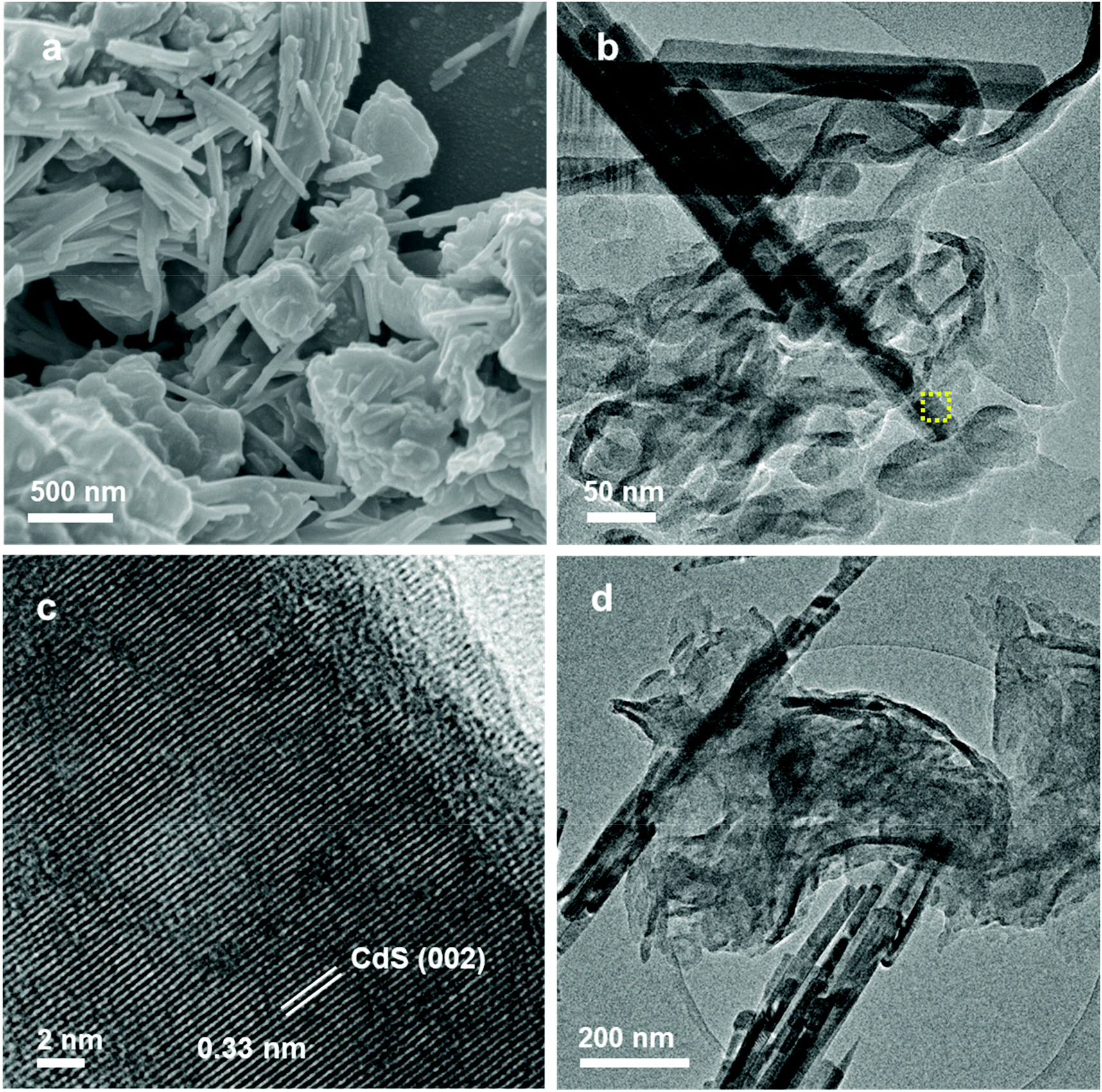 | ||
| Fig. 1 Morphologies of CS/CN-II and CS/CN-Z. (a) FESEM image, (b) TEM image and (c) HRTEM image of CS/CN-II ((c) is the close-up of the marked areas (yellow dashed line) in (b)). (d) TEM image of CS/CN-Z. | ||
The composition and chemical valence of the as-prepared samples were analyzed by XPS. The survey spectra in Fig. S3† confirm the presence of elements in the pure and composite materials. High-resolution XPS spectra were obtained for CS/CN-II. In the C 1s spectra (Fig. S4a†), the peak located at 284.7 eV for CS/CN-II is ascribed to the sp2 C–C bonds in g-C3N4. The peak at 288.2 eV corresponds to the hybridized carbon in N–C![[double bond, length as m-dash]](https://www.rsc.org/images/entities/char_e001.gif) N.32 Fig. S4b† shows the N 1s spectra which are deconvoluted into three peaks. The peaks at 398.7 eV, 399.7 eV and 400.8 eV can be assigned to the sp2-bonded N in the triazine rings (C–NC), tertiary nitrogen (N–(C)3) and amino functional groups (C–N–H), respectively.33 The characteristic bands for Cd 3d at 405.3 eV and 412.0 eV further confirm that the chemical valence state of the Cd element is Cd2+ (Fig. S4c†). The S 2p peaks at 161.5 eV and 162.8 eV belong to the S2− ions in CdS nanorods (Fig. S4d†). Besides, it can be noticed that the XPS peaks of CS/CN-II have a slight shift to the high-energy region compared to those of pure CdS and g-C3N4. This is attributed to the formation of heterojunctions with a tight interface between the two components in CS/CN-II.18
N.32 Fig. S4b† shows the N 1s spectra which are deconvoluted into three peaks. The peaks at 398.7 eV, 399.7 eV and 400.8 eV can be assigned to the sp2-bonded N in the triazine rings (C–NC), tertiary nitrogen (N–(C)3) and amino functional groups (C–N–H), respectively.33 The characteristic bands for Cd 3d at 405.3 eV and 412.0 eV further confirm that the chemical valence state of the Cd element is Cd2+ (Fig. S4c†). The S 2p peaks at 161.5 eV and 162.8 eV belong to the S2− ions in CdS nanorods (Fig. S4d†). Besides, it can be noticed that the XPS peaks of CS/CN-II have a slight shift to the high-energy region compared to those of pure CdS and g-C3N4. This is attributed to the formation of heterojunctions with a tight interface between the two components in CS/CN-II.18
The interaction of CdS nanorods with g-C3N4 nanosheets was also investigated by FTIR. In Fig. 2a, for pure CdS, the absorption bands located in the ranges of 700–820 cm−1 and 1250–1660 cm−1 arise from the Cd–S bonds.34,35 For pure g-C3N4, the broad band at 3150 cm−1 belongs to the stretching mode of the N–H bonds. The characteristic bands between 1200 and 1750 cm−1 are related to the skeletal stretching vibration of aromatic g-C3N4 heterocycles.36 Additionally, the band located at 809 cm−1 is ascribed to the out-of-plane bending vibration mode of g-C3N4 triazine rings.31 For the CdS/g-C3N4 composites, it is worth noting that this vibration mode has red shifts of 3 cm−1 and 13 cm−1 for CS/CN-Z and CS/CN-II, respectively (inset of Fig. 2a). The red shift of this characteristic band suggests that the bond strengths of C–N and CN are weakened due to the strong interaction between CdS and g-C3N4.37 As the CS/CN-Z sample was prepared through the chemisorption and self-assembly method by mechanically mixing at room temperature, a weak interaction was found between the two compounds, resulting in a small red shift of the characteristic band. In contrast, the CS/CN-II sample has a large red shift of 13 cm−1. This is probably because the thermal treatment (300 °C) in the synthetic process could provide an intense binding strength between CdS and g-C3N4, which weakens the bonds between the C and N atoms. Therefore, both FTIR spectra and XPS results demonstrate that a closely contacted interface and an intense interaction between CdS and g-C3N4 were developed in CS/CN-II, which are stronger than those developed in CS/CN-Z.
 | ||
| Fig. 2 Physicochemical and photophysical properties of the as-prepared samples. (a) FTIR spectra (inset: enlarged spectra in the range of 865–740 cm−1), (b) UV-vis DRS spectra, (c) transient photocurrent density and (d) EIS spectra of CdS, g-C3N4, CS/CN-II and CS/CN-Z. | ||
The optical absorption spectra obtained by UV-vis DRS are shown in Fig. 2b. Pure g-C3N4 and CdS exhibit the absorption edges at 435 and 525 nm, respectively, due to their intrinsic electronic properties. For composite materials, the incorporation of CdS plays a key role in sensitizing g-C3N4 and improving its optical response to visible light. Hence, the absorptions of CS/CN-II and CS/CN-Z are notably extended to the visible light region due to synergistic absorption. Compared to the physically mixed CdS/g-C3N4 sample with an absorption threshold of 507 nm, the absorption edges of CS/CN-Z and CS/CN-II are red-shifted to 512 and 521 nm, respectively which are close to that of CdS (Fig. S5†). This proves the formation of heterojunctions at the interface of CdS and g-C3N4 and the more intense interaction leads to a larger band edge shift. The bandgap energies (Eg) of CdS and g-C3N4 were obtained by fitting the DRS data using the Tauc/Davis–Mott model.38 As revealed by the Tauc plot in Fig. S6,† the bandgap energies of CdS and g-C3N4 were found to be 2.36 and 2.85 eV, respectively. The bandgap energies of the composite materials are between those of CdS and g-C3N4, and closer to that of CdS due to the photosensitization by CdS. Moreover, the valence band (VB) potential (EVB) was measured by UPS. In Fig. S7a and S7b,† the VB top positions of CdS and g-C3N4 were measured to be 1.83 and 1.64 eV, respectively versus the Fermi levels of the samples. Therefore, based on the formula Eg = EVB − ECB, the conduction band (CB) potentials (ECB) of CdS and g-C3N4 are found to be −0.53 and −1.21 eV. Besides, the ECB and EVB values of CdS and g-C3N4 can be also determined by the following equations:39
| E′CB = χ − Ee − 1/2Eg | (1) |
| E′VB = Eg + E′CB | (2) |
The transient photocurrent was measured to study the charge separation properties of photocatalysts. As shown in Fig. 2c, all the samples exhibit a reproducible photocurrent during each ON/OFF irradiation cycle. The composite materials show a higher photocurrent density than those of pure CdS and g-C3N4. This indicates that the formation of heterojunctions can significantly improve the charge separation. CS/CN-II possesses the highest photocurrent density, which is about 23% higher than that of CS/CN-Z. This result demonstrates that the type II heterostructure of CdS/g-C3N4 has a superior charge separation ability to the Z-scheme one. Furthermore, the electron impedance spectroscopy (EIS) study provides the information of charge migration kinetics at the photoelectrode/electrolyte interface. Generally, the smaller arc radius of EIS spectra indicates the lower charge migration resistance and faster charge transfer rate at the interface.40 In Fig. 2d, the CS/CN-II sample has the smallest arc radius among the samples, suggesting the lowest interfacial charge transfer resistance. The large radius of g-C3N4 can be attributed to the low electrical conductivity of the C–N network. The results of photocurrent and EIS spectra exhibit a similar trend, which signifies that the construction of heterojunctions can efficiently facilitate the charge separation and transportation, The type II composite shows a superior photoelectrochemical performance to the Z-scheme system. Such properties would eventually have a significant impact on their photocatalytic activities.
3.2. Photocatalytic activity
The photocatalytic activity was evaluated in a closed gas circulation system under visible light illumination (λ > 400 nm). To optimize the conditions of photoreactions, H2 generation was first measured in aqueous solutions containing different scavengers such as methanol, lactic acid, triethanolamine (TEOA) and Na2S/Na2SO3 solutions. In Fig. S8,† the photocatalyst in a 20 vol% lactic acid solution (pH = 3) exhibits the highest H2 evolution, suggesting that lactic acid is the optimal sacrificial reagent for the as-prepared samples. This is consistent with the conclusions reported by previous works, in which lactic acid was used as a hole scavenger for CdS-based photocatalysts.36,41–43 As shown in Fig. 3a, CS/CN-II exhibits the highest H2 generation rate of 2410 μmol h−1 g−1 with 1 wt% Pt loaded as a cocatalyst. The evolution rate is 33% higher than that of CS/CN-Z and about 11 times that of pure g-C3N4. It is not surprising to note that the trend of H2 production of the samples is in good agreement with those of photocurrent and EIS (Fig. 2c and d). The excellent charge separation and rapid charge migration in CS/CN-II lead to a remarkable H2 generation activity. The performance is better than or comparable to some of the best CdS/g-C3N4 photocatalysts reported for visible-light-driven H2 generation (Table S1†). Pure CdS exhibits much higher photocatalytic performance than that of g-C3N4 due to the extended visible light absorption (Fig. 2b). The stabilities of H2 generation on CS/CN-II, CS/CN-Z and CdS were tested for four consecutive runs under the same conditions. In Fig. 3b, the photocatalytic activity of CS/CN-II decreased 12% after four runs, indicating a good stability of CS/CN-II. In contrast, after 24 h reaction, the performances of CS/CN-Z and CdS decreased by 29% and 44%, respectively (Fig. 3c and d). The decrease in the activity of CdS-based catalysts is mainly attributed to the accumulation of photogenerated h+ on CdS.44 S2− ions are very susceptible to oxidization by h+ during the photoreaction. CS/CN-II has a good stability because h+ migrate from the CdS VB to the g-C3N4 VB, which will be discussed in the later parts. Hence, photocorrosion can be effectively suppressed when h+ transport away from the sulfide. For CS/CN-Z and pure CdS, the photo-oxidation reaction mainly occurs at CdS which makes the photocatalyst very unstable, leading to a severe photocorrosion and activity decrease. | ||
| Fig. 3 Photocatalytic activity and stability of the samples. (a) Photocatalytic H2 generation for 6 h over the as-prepared samples (50 mg of photocatalysts, 1 wt% Pt, 20 vol% lactic acid, 300 W Xe lamp, >400 nm). Stability tests of (b) CS/CN-II, (c) CS/CN-Z and (d) CdS under the same conditions. | ||
3.3. Photo-deposition of Pt/PbO2 on CS/CN-II and CS/CN-Z
To study the charge separation properties of CdS/g-C3N4 composites, photoreduction and photo-oxidation probing reactions were performed to monitor the photogenerated e− and h+ distributions. HAADF STEM and high-resolution TEM (HRTEM) images were obtained for CS/CN-II loaded with 1 wt% Pt. As shown in Fig. 4a and b and S9a,† the Pt nanoparticles evolved from the photoreduction of Pt4+ by electrons were located on CdS nanorods. The lattice spacing of 0.225 nm is assigned to the (111) plane of metallic Pt and the planar space of 0.33 nm corresponds to CdS (002) planes (Fig. S9a†). This confirms that Pt nanoparticles are loaded on the CdS surface due to the accumulated electrons. Correspondingly, to probe the distribution of photo-excited h+, photo-deposition of PbO2 was also conducted. PbO2 is formed by photo-oxidation of Pb2+ with IO3− used as an electron scavenger. In Fig. 4c and S9b,† it can be seen that the PbO2 clusters are selectively deposited on g-C3N4 nanosheets, especially at the edge positions. This suggests that holes preferentially accumulate at the edge of g-C3N4 rather than the basal planes, leading to a higher reactivity of edges than that of basal planes. The lattice spacing of 0.28 nm in the HRTEM image can be ascribed to the (101) planes of PbO2 (inset of Fig. S9b†). The results of probing reactions demonstrate that the photo-induced e− and h+ are spatially separated on CS/CN-II. Electrons transfer to the CB of CdS which is ready for the photoreduction reactions (i.e., formation of metallic Pt or H2 generation). Meanwhile, the holes flow to the VB of g-C3N4 accounting for the photo-oxidation reactions (i.e., oxidation of Pb2+ or sacrificial reagents). These results confirm the formation of a type II heterostructure in CS/CN-II. Furthermore, the probing reactions were also performed on CS/CN-Z. As shown in Fig. S9c,† Pt nanoparticles with (111) facets were deposited on the g-C3N4 nanosheets. The HAADF image in Fig. 4d clearly shows that numerous tiny Pt nanoparticles were selectively distributed on g-C3N4 instead of CdS. More Pt nanoparticles are found at the edge of g-C3N4 with fewer identified at the basal planes. This demonstrates that the edge of g-C3N4 could facilitate localizing the electrons and anchoring Pt nanoparticles, which act as active sites for photoreduction reactions. Moreover, the PbO2 clusters with (101) facets were located on the CdS nanorods (Fig. 4e and S9d†). Therefore, it can be concluded that the electrons are distributed at the CB of g-C3N4 and the holes are located at the VB of CdS for CS/CN-Z. Charge extinction may exist in CS/CN-Z through recombination of e− at the CdS CB and h+ at the g-C3N4 VB. Although spatial charge separation is achieved by CS/CN-Z, it has a different charge separation mechanism and transfer route compared to CS/CN-II. | ||
| Fig. 4 Charge distribution on CS/CN-II and CS/CN-Z. HAADF images of CS/CN-II with (a and b) 1 wt% Pt and (c) 3 wt% PbO2 loaded, and CS/CN-Z with (d) 1 wt% Pt and (e) 3 wt% PbO2 loaded. | ||
XPS analysis was conducted to analyze the chemical valence of Pt and Pb after the photoreactions. Since metallic Pt0 is regarded as the active site for photocatalytic H2 generation,45 its percentage in the Pt species will largely affect the photocatalytic activity. As shown in Fig. S10a and S10b,† the two main bands located at 71.1 and 74.3 eV are ascribed to the Pt 4f7/2 and Pt 4f5/2 of Pt0, respectively. The spectra demonstrate that most of the Pt species loaded on CS/CN-II and CS/CN-Z exist in the form of Pt0. The shoulder peaks at 72.4 and 75.6 eV which belong to the Pt 4f of Pt2+ species indicate a small portion of Pt4+ was partially reduced to Pt2+. In Table S2,† based on the XPS and ICP results, the actual percentage of Pt0 loading in CS/CN-II is 0.69 wt%, which is 23% higher than that of CS/CN-Z (0.56 wt%). This may result in a higher photocatalytic performance of CS/CN-II due to the more Pt0 reactive sites. Fig. S10c and S10d† show the Pb species loaded on CS/CN-II and CS/CN-Z after the photo-deposition. The two main peaks at 137.4 and 142.3 eV correspond to the Pb 4f7/2 and Pb 4f5/2 of Pb4+, respectively. It suggests that most of Pb2+ was oxidized to Pb4+ on both samples. Less amount of Pb2+ exists in the samples which is evidenced by the shoulder peaks at 138.7 and 143.5 eV. Higher percentages of Pt0 and Pb4+ species on CS/CN-II indicate a superior charge separation efficiency, which is consistent with the photocurrent result (Fig. 2c). More photo-excited e− and h+ are spatially separated and available for photoredox reactions in CS/CN-II. Such properties accounts for the excellent photocatalytic H2 generation activity of CS/CN-II.
3.4. SRM study of charge distribution at single-turnover resolution
To study the charge distribution and photocatalytic heterogeneity at single-turnover resolution, super-resolution fluorescence microscopy was used to visualize the photoreactions (Fig. 5a). Fluorogenic reactions were designed to obtain the mappings of photo-excited e− and h+, in which the non-fluorescent reactants are catalyzed to highly fluorescent products. The photoreduction of non-fluorescent resazurin to fluorescent resorufin can be applied to localize the electrons.25 Correspondingly, photogenerated h+ can be detected by an indirect mechanism, in which non-fluorescent Amplex Red can be oxidized to resorufin by ˙OH produced from the reaction between holes and adsorbed H2O.26 Hence, each fluorescence burst observed in the SRM image originates from a single photocatalytic turnover which leads to the formation of a fluorescent resorufin molecule at a reactive site (Fig. 5b). As shown in the intensity trajectory in Fig. 5c, τoff represents the waiting time before the formation of each resorufin molecule, while τon signifies the residence time of resorufin on the catalyst surface before dissociation. Thus, the one-step ON/OFF change of fluorescence signals with low background in Fig. 5c suggests the stochastic single-turnover events. By recording the locations of millions of catalytic events, all the single-molecule frames containing fluorescent bursts were integrated and fitted by point spread function. Consequently, SRM images can be reconstructed with a spatial resolution of 16 nm (Fig. S11†). Fig. S12† shows the brightfield images, SRM images and density maps of pure CdS nanorods with resazurin. The SRM images provide the information of super-localization of photoactive species and reactive sites with nanometer-scale precision. The density maps processed from SRM images clearly demonstrate the density of these species, catalytic reactivity and heterogeneity at different locations. Under laser excitation, the fluorescent bursts of resorufin are mainly located at the end segments of CdS nanorods and detected less at the central parts, as shown at the positions 1, 2, 3, and 4 in Fig. S12.† This demonstrates that the separated electrons are predominantly distributed at the ends of CdS nanorods, indicating a higher reactivity at this region. Such phenomena are likely due to the low-coordination environment and disordered structure at the end segments, which can be observed from the positions 1, 2, and 3 in Fig. S2b.† The regions such as defects, terrace, kinks, steps and corner sites are believed to have a higher catalytic performance owing to the high coordinative unsaturation.46–48 Fig. S13† shows the morphologies of CdS before and after illumination with Amplex Red. The CdS nanorods suffer from severe photocorrosion when h+ are localized and react with Amplex Red. Hence, the morphology of CdS totally changed after irradiation (Fig. S13b†) and no SRM images can be obtained. For pure g-C3N4, it was found that the fluorescent bursts of resazurin photoreduction mostly take place at the edges of nanosheets, suggesting the photogenerated e− migrated and concentrated at this position (Fig. S14†). Moreover, the fluorescent spots generated from the photo-oxidation of Amplex Red mainly emerged at the central parts of g-C3N4 nanosheets (Fig. S15†). This indicates that the h+ are mostly distributed at the basal planes of nanosheets. Therefore, spatial charge separation can be also achieved and observed on pure g-C3N4. | ||
| Fig. 5 Super-resolution imaging of charge locations using fluorescent probes. (a) Schematic of total internal reflection fluorescence microscopy. (b) A single-frame image of fluorescent resorufin molecules (in yellow circles) on CdS nanorods. Scale bar: 1 μm. (c) Typical fluorescence intensity trajectory for an area of 500 nm × 500 nm in the marked green square in (b) (bin time: 30 ms). | ||
The SRM images were also obtained for CdS/g-C3N4 nanocomposites to study the charge flow and distribution. In Fig. 6a–c, the fluorescent bursts on CS/CN-II from resazurin photoreduction mainly occurred at CdS nanorods, suggesting the diffusion direction and preferred location of photo-induced electrons. More electrons are found at the end segments of CdS than the central parts, which is also observed for pure CdS (Fig. S12†). Correspondingly, the h+ are found to be distributed at the edges of g-C3N4 as shown in Fig. 6d–f. It has been reported that the charge (i.e., e− and h+) density at the edge of g-C3N4/N-doped graphene is higher than that of basal planes owing to the higher local curvature of edges than that of basal planes.49 A similar phenomenon was also observed for other 2D layered materials using the SRM method.50 With electrons flowing to CdS in the composite, the holes would preferentially locate at the edge position of g-C3N4 in CS/CN-II. The reason why holes are located at the basal planes of pure g-C3N4 is possibly because electrons are preferable to occupy the high curvature sites at edges without the heterojunction structure.51 Future studies are needed to further clarify the detailed mechanism of charge distribution and catalytic events on pure 2D nanosheets. Fig. 7 shows the conventional images, SRM images and density maps of CS/CN-Z with resazurin. Under laser excitation, the fluorescent spots which represent the locations of photo-induced e− are distributed at the edges of g-C3N4 nanosheets. This result suggests that the electrons are accumulated at g-C3N4 in CS/CN-Z. However, the photo-oxidation of Amplex Red on CS/CN-Z leads to the photocorrosion of CdS in the composite, as indicated in the conventional images of CS/CN-Z before and after laser irradiation (Fig. S16†). This indicates that the h+ are located at CdS, which proves the Z-scheme structure of CS/CN-Z. Therefore, the super-resolution mapping results clearly reveal the surface reactive sites at the nanoscale and elucidate the two charge separation mechanisms of CS/CN-II and CS/CN-Z.
 | ||
| Fig. 6 Single-molecule SRM of CS/CN-II at single-turnover resolution. Conventional brightfield images, SRM images and density maps of CS/CN-II with (a–c) resazurin (inset: the close-up of the marked area (orange dashed line) in (c), bin size: 10 nm × 10 nm) and (d–f) Amplex Red (bin size: 25 nm × 25 nm). Scale bar: 1 μm. | ||
 | ||
| Fig. 7 Single-molecule SRM of CS/CN-Z at single-turnover resolution. (a) Conventional brightfield images, (b) SRM images and (c) density maps (bin size: 25 nm × 25 nm) of CS/CN-Z with resazurin. Scale bar: 1 μm. | ||
Based on the charge tracking results of photo-deposition and super-resolution fluorescence imaging, two charge transfer routes were confirmed for CS/CN-II and CS/CN-Z. In Scheme 1a, the band alignment of CdS and g-C3N4 in CS/CN-II makes the charges migrate in the opposite direction, leading to an efficient spatial charge separation. Charge extinction can be significantly suppressed through this configuration which contributes to the excellent photocatalytic performance and stability of CS/CN-II. In contrast, CS/CN-Z exhibits a different charge transfer route with charge recombination present between the CdS CB and the g-C3N4 VB (Scheme 1b). Hence, the charge separation efficiency is expected to be lower than that of CS/CN-II. Besides. as shown in Fig. S7c,† CS/CN-II exhibits a VB potential of 1.71 eV, which is closer to the g-C3N4 VB (1.64 eV). This implies that the h+ in the composite rapidly transfer to the VB of g-C3N4. In contrast, the VB potential of CS/CN-Z (1.77 eV) is found to be closer to that of CdS (1.83 eV), indicating the accumulation of h+ on the CdS VB (Fig. S7d†). Despite the stronger oxidative VB potential of CS/CN-Z compared to CS/CN-II, the photocatalytic performance is inferior to CS/CN-II (Fig. 3a). This is because the poor charge separation efficiency and serious photocorrosion in CS/CN-Z act as the main factors limiting the photocatalytic efficiency and stability. Although CS/CN-II and CS/CN-Z have the same content of CdS and g-C3N4, two distinct heterostructures were formed due to the different synthetic routes. As revealed by the FTIR and XPS results (Fig. 2a and S4†), an intense interaction between CdS and g-C3N4 was developed in CS/CN-II because of thermal calcination at 300 °C. The closely contacted interface is a key prerequisite and can promote the kinetic flow of charges between the two components. In the case of CS/CN-Z, which was prepared by the self-assembly method at room temperature, the charges do not prefer to transfer kinetically and tend to stay at their own electronic band due to the weak interaction. Furthermore, it was found that CdS in CS/CN-II at the interface position is more crystalline than that in CS/CN-Z. As shown in the HRTEM images in Fig. S17a,† the highly crystalline CdS at the interface was observed for CS/CN-II due to calcination. However, some disordered areas which contain bulk defects were identified for CS/CN-Z (Fig. S17b†). The bulk defects could act as deep trapping sites for photogenerated e− and h+ and retard their mobility, leading to the formation of charge recombination centers at these sites. In contrast, a well-ordered crystalline structure of CdS at the interface of CS/CN-II facilitates rapid charge transportation to the catalyst surface for redox reactions. The notably enhanced crystallinity of CS/CN-II can be also verified by the XRD results (Fig. S1†). Therefore, the more intense interaction and the enhanced crystalline structure in CS/CN-II due to thermal calcination account for the efficient interfacial charge transfer and separation. Hence, based on the above discussion, our work demonstrates a direct imaging method to visualize and map the photoactive species in composites at the nanoscale. It provides an in-depth understanding of charge distribution and energy flows in two distinct heterostructures and correlates these properties with the photocatalytic activity. We expect that this study would benefit the rational design of type II and Z-scheme composites, intended for efficient photocatalytic applications.
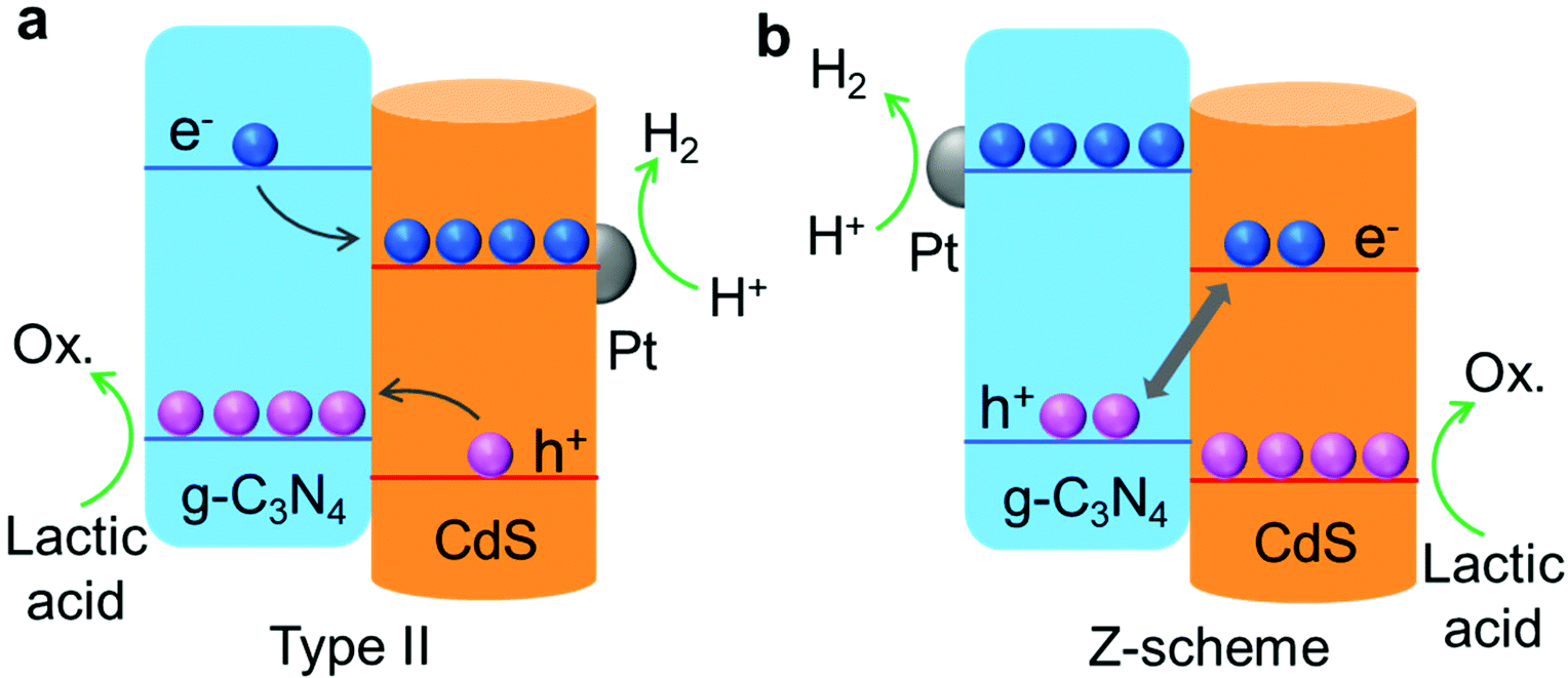 | ||
| Scheme 1 Schematic of charge transfer and photocatalytic reactions on (a) CS/CN-II and (b) CS/CN-Z. | ||
4. Conclusion
In conclusion, we applied the techniques of HRTEM, HAADF STEM and SRM to investigate the charge separation mechanisms of type II and Z-scheme CdS/g-C3N4 composites. Different charge transfer routes were observed for the two heterostructures. In particular, the SRM method was used for the first time to map the photoactive sites on type II and Z-scheme heterojunctions at the nanoscale. It was found that the photo-excited electrons are predominantly located at the two end segments of CdS nanorods while the photoactive species are accumulated at the edges of g-C3N4. As revealed by the photoactivity measurement, type II heterostructure of CdS/g-C3N4 exhibits a superior photocatalytic performance to the Z-scheme one, due to the higher charge separation efficiency and less photocorrosion. Therefore, this work is essential for the following reasons. First, through combining the microscopic study with the bulk activity measurement, our findings provide a deep insight into the understanding of “structure–activity” correlations in nanocomposites. Second, it enables us to potentially control the energy and charge flows and engineer the reactive sites in these materials. Third, such investigation would benefit the electronic band modulation and interface engineering of heterogeneous catalysts, leading to an enhancement of photocatalytic activity under visible light.Conflicts of interest
There are no conflicts to declare.Acknowledgements
We acknowledge the financial support from the Ministry of Education, Singapore, under its Academic Research Fund Tier 1 (No. RG10/20), and the Singapore Agency for Science, Technology and Research (A*STAR) AME YIRG grant (No. A2084c0065). We also would like to thank Haojing Wang for her help in photoelectrochemical measurements.References
- A. Fujishima and K. Honda, Nature, 1972, 238, 37–38 CrossRef CAS PubMed.
- Y. Liu, X. Zeng, X. Hu, J. Hu and X. Zhang, J. Chem. Technol. Biotechnol., 2019, 94, 22–37 CrossRef CAS.
- C. Tan, X. Cao, X.-J. Wu, Q. He, J. Yang, X. Zhang, J. Chen, W. Zhao, S. Han and G.-H. Nam, Chem. Rev., 2017, 117, 6225–6331 CrossRef CAS PubMed.
- Y. Zhu, Y. Feng, S. Chen, M. Ding and J. Yao, J. Mater. Chem. A, 2020, 8, 25626–25648 RSC.
- X. Zhang, X. Yuan, L. Jiang, J. Zhang, H. Yu, H. Wang and G. Zeng, Chem. Eng. J., 2020, 390, 124475 CrossRef CAS.
- Y. Lu, H. Wang, P. Yu, Y. Yuan, R. Shahbazian-Yassar, Y. Sheng, S. Wu, W. Tu, G. Liu and M. Kraft, Nano Energy, 2020, 77, 105158 CrossRef CAS.
- W. Tu, Y. Xu, J. Wang, B. Zhang, T. Zhou, S. Yin, S. Wu, C. Li, Y. Huang, Y. Zhou, Z. Zou, M. Kraft and R. Xu, ACS Sustainable Chem. Eng., 2017, 5, 7260–7268 CrossRef CAS.
- J. Liang, X. Yang, Y. Wang, P. He, H. Fu, Y. Zhao, Q. Zou and X. An, J. Mater. Chem. A, 2021, 9, 12898–12922 RSC.
- Y. Ni, R. Wang, W. Zhang, S. Shi, W. Zhu, M. Liu, C. Yang, X. Xie and J. Wang, Chem. Eng. J., 2021, 404, 126528 CrossRef CAS.
- N. Feng, H. Lin, F. Deng and J. Ye, J. Phys. Chem. C, 2021, 125, 12012–12018 CrossRef CAS.
- X. Zhao, Y. Fan, W. Zhang, X. Zhang, D. Han, L. Niu and A. Ivaska, ACS Catal., 2020, 10, 6367–6376 CrossRef CAS.
- Y. Luo, J. Qin, G. Yang, S. Luo, Z. Zhao, M. Chen and J. Ma, Chem. Eng. J., 2021, 410, 128394 CrossRef CAS.
- N. Güy, Appl. Surf. Sci., 2020, 522, 146442 CrossRef.
- Y. Chen, F. Wang, Y. Cao, F. Zhang, Y. Zou, Z. Huang, L. Ye and Y. Zhou, ACS Appl. Energy Mater., 2020, 3, 4610–4618 CrossRef CAS.
- Z. Shi, Y. Zhang, X. Shen, G. Duoerkun, B. Zhu, L. Zhang, M. Li and Z. Chen, Chem. Eng. J., 2020, 386, 124010 CrossRef CAS.
- Y. Wang, H. Huang, Z. Zhang, C. Wang, Y. Yang, Q. Li and D. Xu, Appl. Catal., B, 2021, 282, 119570 CrossRef CAS.
- M. Zhang, C. Lai, B. Li, F. Xu, D. Huang, S. Liu, L. Qin, X. Liu, H. Yi and Y. Fu, Chem. Eng. J., 2021, 422, 130120 CrossRef CAS.
- X. Zhou, Y. Fang, X. Cai, S. Zhang, S. Yang, H. Wang, X. Zhong and Y. Fang, ACS Appl. Mater. Interfaces, 2020, 12, 20579–20588 CrossRef CAS PubMed.
- G. Li, B. Wang, J. Zhang, R. Wang and H. Liu, Appl. Surf. Sci., 2019, 478, 1056–1064 CrossRef CAS.
- D. P. Kumar, S. Hong, D. A. Reddy and T. K. Kim, J. Mater. Chem. A, 2016, 4, 18551–18558 RSC.
- J. Pan, P. Wang, P. Wang, Q. Yu, J. Wang, C. Song, Y. Zheng and C. Li, Chem. Eng. J., 2021, 405, 126622 CrossRef CAS.
- N.-N. Vu, S. Kaliaguine and T.-O. Do, ACS Appl. Energy Mater., 2020, 3, 6422–6433 CrossRef CAS.
- M. J. Rust, M. Bates and X. Zhuang, Nat. Methods, 2006, 3, 793–796 CrossRef CAS PubMed.
- A. Sharonov and R. M. Hochstrasser, Proc. Natl. Acad. Sci. U. S. A., 2006, 103, 18911–18916 CrossRef CAS PubMed.
- J. B. Sambur, T.-Y. Chen, E. Choudhary, G. Chen, E. J. Nissen, E. M. Thomas, N. Zou and P. Chen, Nature, 2016, 530, 77–80 CrossRef CAS PubMed.
- J. W. Ha, T. P. A. Ruberu, R. Han, B. Dong, J. Vela and N. Fang, J. Am. Chem. Soc., 2014, 136, 1398–1408 CrossRef CAS PubMed.
- M. Shi, G. Li, J. Li, X. Jin, X. Tao, B. Zeng, E. A. Pidko, R. Li and C. Li, Angew. Chem., Int. Ed., 2020, 59, 6590–6595 CrossRef CAS PubMed.
- J. Liu, T. Zhang, Z. Wang, G. Dawson and W. Chen, J. Mater. Chem., 2011, 21, 14398–14401 RSC.
- L. J. Zhang, T. F. Xie, D. J. Wang, S. Li, L. L. Wang, L. P. Chen and Y. C. Lu, Int. J. Hydrogen Energy, 2013, 38, 11811–11817 CrossRef CAS.
- Y. Li, X. Wei, H. Li, R. Wang, J. Feng, H. Yun and A. Zhou, RSC Adv., 2015, 5, 14074–14080 RSC.
- M. Lu, Z. Pei, S. Weng, W. Feng, Z. Fang, Z. Zheng, M. Huang and P. Liu, Phys. Chem. Chem. Phys., 2014, 16, 21280–21288 RSC.
- P. Wang, T. Wu, C. Wang, J. Hou, J. Qian and Y. Ao, ACS Sustainable Chem. Eng., 2017, 5, 7670–7677 CrossRef CAS.
- H. He, J. Cao, M. Guo, H. Lin, J. Zhang, Y. Chen and S. Chen, Appl. Catal., B, 2019, 249, 246–256 CrossRef CAS.
- L. Ge, F. Zuo, J. Liu, Q. Ma, C. Wang, D. Sun, L. Bartels and P. Feng, J. Phys. Chem. C, 2012, 116, 13708–13714 CrossRef CAS.
- B. Chong, L. Chen, D. Han, L. Wang, L. Feng, Q. Li, C. Li and W. Wang, Chin. J. Catal., 2019, 40, 959–968 CrossRef CAS.
- Z. Wang, Z. Wang, X. Zhu, C. Ai, Y. Zeng, W. Shi, X. Zhang, H. Zhang, H. Si and J. Li, Small, 2021, 2102699 CrossRef CAS PubMed.
- X. Liu, Y. Liu, W. Zhang, Q. Zhong and X. Ma, Mater. Sci. Semicond. Process., 2020, 105, 104734 CrossRef CAS.
- Y. Xu, Y. Li, P. Wang, X. Wang and H. Yu, Appl. Surf. Sci., 2018, 430, 176–183 CrossRef CAS.
- Y. Xu and M. A. Schoonen, Am. Mineral., 2000, 85, 543–556 CrossRef CAS.
- S. Wu, W. Wang, W. Tu, S. Yin, Y. Sheng, M. Y. Manuputty, M. Kraft and R. Xu, ACS Sustainable Chem. Eng., 2018, 6, 14470–14479 CrossRef CAS.
- W. Li, C. Feng, S. Dai, J. Yue, F. Hua and H. Hou, Appl. Catal., B, 2015, 168, 465–471 CrossRef.
- L. Qian, Y. Hou, Z. Yu, M. Li, F. Li, L. Sun, W. Luo and G. Pan, Mol. Catal., 2018, 458, 43–51 CrossRef CAS.
- S. Yin, J. Han, Y. Zou, T. Zhou and R. Xu, Nanoscale, 2016, 8, 14438–14447 RSC.
- X. Ning and G. Lu, Nanoscale, 2020, 12, 1213–1223 RSC.
- S. Wu, M. Y. Manuputty, Y. Sheng, H. Wang, Y. Yan, M. Kraft and R. Xu, Small Methods, 2021, 5, 2000928 CrossRef CAS PubMed.
- M. J. K. Ow, J. J. Ng, J. X. Yong, B. Y. L. Quek, E. K. Yeow and Z. Zhang, ACS Appl. Nano Mater., 2020, 3, 3163–3167 CrossRef CAS.
- L. Liu and A. Corma, Chem. Rev., 2018, 118, 4981–5079 CrossRef CAS PubMed.
- X. Zhou, N. M. Andoy, G. Liu, E. Choudhary, K.-S. Han, H. Shen and P. Chen, Nat. Nanotechnol., 2012, 7, 237–241 CrossRef CAS PubMed.
- C. Xu, S. Wu, G. Xiong, X. Guo, H. Yang, J. Yan, K. Cen, Z. Bo and K. K. Ostrikov, Appl. Catal., B, 2021, 280, 119461 CrossRef CAS.
- T.-X. Huang, B. Dong, S. L. Filbrun, A. A. Okmi, X. Cheng, M. Yang, N. Mansour, S. Lei and N. Fang, Sci. Adv., 2021, 7, eabj4452 CrossRef CAS PubMed.
- J. Yang, Y. Liu, D. Zhang, X. Wang, R. Li and Y. Li, Nano Res., 2015, 8, 3054–3065 CrossRef CAS.
Footnote |
| † Electronic supplementary information (ESI) available. See DOI: http://doi.org/10.1039/d2nr00316c |
| This journal is © The Royal Society of Chemistry 2022 |