
Two-dimensional cobalt telluride as a piezo-tribogenerator†
Solomon Demiss
Negedu‡
 ab,
Raphael
Tromer‡
c,
Chinmayee Chowde
Gowda
d,
Cristiano F.
Woellner
e,
Femi Emmanuel
Olu
b,
Ajit K.
Roy
f,
Prafull
Pandey
g,
Douglas S.
Galvao
*ch,
Pulickel M.
Ajayan
*i,
Partha
Kumbhakar
*a and
Chandra S.
Tiwary
*a
ab,
Raphael
Tromer‡
c,
Chinmayee Chowde
Gowda
d,
Cristiano F.
Woellner
e,
Femi Emmanuel
Olu
b,
Ajit K.
Roy
f,
Prafull
Pandey
g,
Douglas S.
Galvao
*ch,
Pulickel M.
Ajayan
*i,
Partha
Kumbhakar
*a and
Chandra S.
Tiwary
*a
aDepartment of Metallurgical and Materials Engineering, Indian Institute of Technology Kharagpur, West Bengal 721302, India. E-mail: parthakumbhakar2@gmail.com; chandra.tiwary@metal.iitkgp.ac.in
bMaterials Science and Engineering, Jimma Institute of Technology, Jimma University, Jimma, Ethiopia
cApplied Physics Department, University of Campinas, Brazil. E-mail: galvao@ifi.unicamp.br
dSchool of Nano Science and Technology, Indian Institute of Technology Kharagpur, West Bengal 721302, India
ePhysics Department, Federal University of Parana, UFPR, Curitiba, PR 81531-980, Brazil
fMaterials and Manufacturing Directorate, Air Force Research Laboratory, Wright Patterson AFB, OH 45433-7718, USA
gDepartment of Materials Engineering, Indian Institute of Science, Bangalore 560012, India
hCenter for Computational Engineering and Sciences, State University of Campinas, Campinas, SP 13083-970, Brazil
iDepartment of Materials Science and Nano Engineering, Rice University, Houston, TX 77005, USA. E-mail: ajayan@rice.edu
First published on 30th March 2022
Abstract
Two-dimensional (2D) materials have been shown to be efficient in energy harvesting. Here, we report the use of waste heat to generate electricity via the combined piezoelectric and triboelectric properties of 2D cobalt telluride (CoTe2). The piezo-triboelectric nanogenerator (PTNG) produced an open-circuit voltage of ∼5 V under 1 N force and the effect of temperature in the range of 305–363 K shows a four-fold energy conversion efficiency improvement. The 2D piezo-tribogenerator shows excellent characteristics with a maximum voltage of ∼10 V, fast response time, and high responsivity. Density functional theory was used to gain further insights and validation of the experimental results. Our results could lead to energy harvesting approaches using 2D materials from various thermal sources and dissipating waste heat from electronic devices.
1. Introduction
The rise in global energy demand has led researchers to explore new sources of green energy, which are environmentally friendly and cost-effective. Self-powered systems based on piezo, tribo, thermo, and pyroelectric phenomena are a good source of green energy.1–5 The energy generated using piezo and triboelectric nanogenerators (with large power densities) is used for small powered appliances such as electronic devices, sensors, and energy harvesting devices.6–11 The need to develop an alternative sustainable energy source is a timely and urgent society demand. Energy harvesting technologies are used to collect energy from different sources around us, such as solar energy, heat, and mechanical energy, and convert into electrical energy. Mechanical energy, on the other hand, is ubiquitous and sufficient in daily life. Although mechanical energy exists abundantly in different forms, a large proportion of them goes unnoticed. Waste heat dissipated from electronic devices is also a form of energy that can be harvested to power electronic devices. Nanogenerators are one such energy harvesting device, which has been developed to convert mechanical energy into electrical energy, providing an effective solution in modern times. Hybrid piezo–triboelectric nanogenerators are a new class of self-powered systems that take advantage of the synergy existing between piezoelectric and triboelectric mechanisms to improve the energy harvesting efficiency and meet the energy and power needs of portable/wearable electronic devices. Devising a nanogenerator to integrate different energy harvesting systems to work at full potential has been a challenge. Self-powered nanogenerators are recently on a rise because of their ability to work without power cables and batteries. The overall power generated is comparatively larger than that of just a nanogenerator working on a single energy generation mechanism.12,13 As the size of electronic devices is reduced, the heat generated during operation is substantial, which can affect the performance of PTNGs. Hence, it is essential to study the efficiency of a PTNG under elevated temperature conditions and explore its utilization to harvest energy.6,14 Recently, considerable innovative research efforts have been dedicated to fabricating piezo/triboelectric nanogenerators using 2D transition metal dichalcogenide (TMDC) materials.14–17 Their well-defined structural topologies, good flexibility, and large surface area make them potential candidates for self-powered systems.17–19 Among TMDCs, tellurides exhibit unique bandgap sensitivity on application of strain, which makes them a better candidate for piezoelectric and triboelectric nanogenerators for energy conversion, storage, and energy harvesting in small electronic devices.19–23 Recently, Ajayan et al. reported the piezoelectric properties of 2D tellurium films (tellurene) due to the presence of Born effective charges.24 Other layered TMDCs such as MX2 (M = Mo and Wo and X = S, Se, and Te) have shown piezoelectricity in their hexagonal forms because of their out-of-plane inversion symmetry.25 Among other layered TMDCs, cobalt-based TMDCs (CoX and CoX2, X = S, Se, and Te) have gained attention due to their catalytic, electrocatalytic, electrical, and magnetic behaviors in low dimensions.26–29 Layered CoTe2 has a hexagonal unit cell and six Te atoms surround each Co atom. 2D materials have been chosen for implementing these piezo/triboelectric nanogenerators due to their transparency, flexibility, and high surface-to-volume ratios, and the possibility of making very thin devices.Here, we demonstrate a high-performance and flexible piezo-triboelectric nanogenerator using 2D CoTe2 as an active material. The device can function as a generator to harvest waste heat and collect mechanical energy from deformations at high temperatures. 2D CoTe2 was synthesized using a simple sonication-assisted liquid exfoliation method from its bulk crystal. A detailed materials characterization using spectroscopy and microscopy has been performed. The energy conversion and energy harvesting properties of 2D CoTe2 have been carefully investigated by carrying out experimental and supporting density functional theory (DFT) calculations. The PTNG fabrication and working mechanism based on temperature dependence and mechanical strain harvesting are shown in Fig. 1. The piezoelectric and triboelectric effects are demonstrated by harvesting mechanical strain (tapping and bending) and heat energy dissipated from various sources (electronic devices). DFT and ab initio molecular dynamics simulations have been used to analyze the temperature-dependent behavior of our PTNG cell under strain conditions. Therefore, utilization of these PTNG devices to effectively harvest energy from such overlooked sources can be realized.
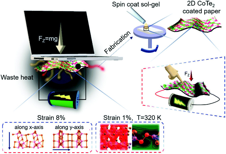 | ||
| Fig. 1 Schematic representation of the utilization of waste heat by generating electricity and the energy harvesting concept of piezo-tribo generators using 2D CoTe2. | ||
2. Experimental
2.1. Synthesis of bulk and exfoliated CoTe2
Bulk CoTe2 was obtained using vacuum induction melting. Metal samples Co and Te (99.99% purity) were used for composite preparation. The stoichiometric composition of the sample was selected based on a Co–Te binary alloy phase diagram, with 17.5 wt% of Co and 82.5 wt% of Te. The alloys were prepared by melting the constituent elements at a temperature of 1050 °C in a quartz tube using a vacuum induction melting method under an argon atmosphere, and the alloys were allowed to cool naturally. A high vacuum condition of 1 × 10⁻⁵ mbarr was maintained inside the melting chamber to ensure high purity and to prevent oxidation. The as-fabricated sample was polished and made ready for further characterization. Initially, the as-fabricated bulk CoTe2 sample was powdered using a mortar and pestle with acetone as the cleaning medium. Later, 2D CoTe2 samples were prepared using a sonication-assisted liquid exfoliation method. 50 mg of the powdered sample was dispersed in 150 ml of isopropyl alcohol (IPA) and ultra-sonicated (probe sonication, f = 30 kHz) for 4 h at room temperature to obtain a suspension of CoTe2 sheets.2.2. Instrumentation
The morphology and thickness of both bulk and 2D CoTe2 samples were characterized using optical microscopy (Leica-DM2500M) and scanning electron microscopy (Jeol JSM-IT300HR) operating at an acceleration voltage of 20 kV and 7.475 nA. X-ray diffraction (XRD) patterns and information on the crystalline phases of the samples were obtained using an X-ray diffractometer (Bruker, D8 Advance) with Cu-Kα radiation with a wavelength (λ) of 1.5406 Å, operating at 40 kV and 40 mA voltage and current, respectively. Powdered XRD patterns of both samples were analyzed and indexed using Pearson's Crystal Database and Panalytical X'pert high score plus software. Raman spectroscopy analyses were carried out using a WITec UHTS Raman spectrometer (WITec, UHTS 300 VIS, Germany) with a laser excitation wavelength of 532 nm at room temperature (RT). The optical absorbance properties of pristine 2D CoTe2 were characterized using a UV-vis spectrometer from 200 up to 800 nm. The optical band gap energy was estimated using the Tauc plot.2.3. Preparation of CoTe2 based nanogenerators
Hybrid nanogenerators were fabricated for both bulk and 2D structures. The three main components of the device are a positive electrode, an active (piezo-triboelectric) material, and a negative electrode. Copper (Cu) tape and aluminium (Al) foil were used as positive and negative electrodes, respectively, and the PTNG was laminated with a transparent tape leaving space for electrode connections. Under continuous stirring, a homogeneous CoTe2 suspension was made by combining the exfoliated CoTe2 sample powder with fast-acting PVA as an adhesive. The concentration of PVA was kept at 10 wt% and the ratio of the slurry mixture was 10![[thin space (1/6-em)]](https://www.rsc.org/images/entities/char_2009.gif) :1 (sample:adhesive). Then, the slurry was spin-coated onto a piece of paper of an active surface area of ∼9 cm2 which was connected to Al foil for establishing external contact. The as-prepared electrodes were dried on a hot plate. The thicknesses of the CoTe2-Al layer are maintained at ∼230 ± 15 μm. On the opposite side, Kapton and Cu electrodes of a similar area were attached. The thickness of the Kapton electrode was 125 ± 10 μm (standard specifications). The entire arrangement of the device was then enclosed using a transparent polythene sheet and secured. The output voltage of the hybrid piezo-tribo nanogenerator was measured using a digital storage oscilloscope (DSO, Tektronix, TBS1072B).
:1 (sample:adhesive). Then, the slurry was spin-coated onto a piece of paper of an active surface area of ∼9 cm2 which was connected to Al foil for establishing external contact. The as-prepared electrodes were dried on a hot plate. The thicknesses of the CoTe2-Al layer are maintained at ∼230 ± 15 μm. On the opposite side, Kapton and Cu electrodes of a similar area were attached. The thickness of the Kapton electrode was 125 ± 10 μm (standard specifications). The entire arrangement of the device was then enclosed using a transparent polythene sheet and secured. The output voltage of the hybrid piezo-tribo nanogenerator was measured using a digital storage oscilloscope (DSO, Tektronix, TBS1072B).
3. Results and discussion
Here we have demonstrated simultaneous energy harvesting using a combination of external strain and waste heat dissipated (Fig. 1). The PTNG consists of atomically thin CoTe2 exhibiting temperature-dependent behavior. The X-ray diffraction patterns of the bulk and exfoliated CoTe2 are shown in Fig. 2a. The indexing of these intense diffraction peaks of bulk crystals and 2D CoTe2 was in the orthorhombic crystal structure of the non-centrosymmetric space group Pnn2 (No. 34) and lattice parameters a = 5.32940 Å, b = 6.32230 Å, and c = 3.90800 Å. We observed two polymorphic phases, 1T in the bulk form and 1H in the case of 2D, as confirmed from XRD result analysis. Based on the XRD data analysis result, a transition from bulk CoTe2 (1T metallic phase) to 2D CoTe2 (1H phase semiconductor) (Fig. S1a†) was observed. Additionally, laser light exposure (inset of Fig. 2a) shows homogeneously dispersed exfoliated CoTe2. Atomic force microscopy (AFM) measurements were used to confirm the formation of atomically thin CoTe2 (Fig. 2b). The thickness was determined from the height profile of the measured histogram plot of the AFM image (Fig. 2c) and was found to be ∼2–4 nm (i.e. 3–5 layers). The as-prepared bulk and pristine 2D CoTe2 samples were subjected to SEM analysis (see the ESI, Fig. S1b and c†). The SEM image confirms the exfoliation of bulk CoTe2 into layered CoTe2 with multilayer stacks (Fig. S2†). Ultrathin sheets are further characterized by bright-field transmission electron microscopy (BF-TEM) imaging of CoTe2. The BF-TEM image (Fig. 2d) shows transparent regions which confirms the overlapping of ultrathin 2D CoTe2 layers. The lateral dimension of the sheet was rectangular and ranged from 100 to 200 nm. From the high-resolution TEM image (Fig. 2e-I) the measured lattice spacing of the exfoliated sample was ∼0.27 nm corresponding to the (120) plane. The fast Fourier transform pattern confirms the orthorhombic structure of CoTe2, as shown in Fig. 2e-II. The EDX analysis (Fig. S3†) shows only the presence of Co and Te with no impurities. Raman spectroscopy was carried out to confirm the formation of ultrathin CoTe2. Fig. 2f shows the Raman spectrum of 2D CoTe2 with characteristic vibration modes, A1, B1, and Eg2 modes. The inset shows multiple modes (two Eg modes and one A1 mode) in the Raman spectrum. The presence of these peaks confirms the formation of a pure phase of CoTe2.30Fig. 2g shows the X-ray photoelectron spectroscopy (XPS) survey spectra of 2D CoTe2 with the characteristic peaks of Co, Te, O, and C in the samples. The de-convoluted XPS peaks of the sample observed for Co 2p (Fig. 2h) at 780 eV and 796 eV corresponding to CoTe2 and other broader peaks were due to surface oxide formation with Co during exfoliation. The peaks in the region of Te 3d (Fig. 2i) were at 576 and 587 eV corresponding to the Te4+ state (Te 3d5/2 and Te 3d3/2). The presence of an oxidized surface is due to the presence of oxygen during exfoliation of the material. The results are in good agreement with previous studies for the same CoTe2 composite structure.31,32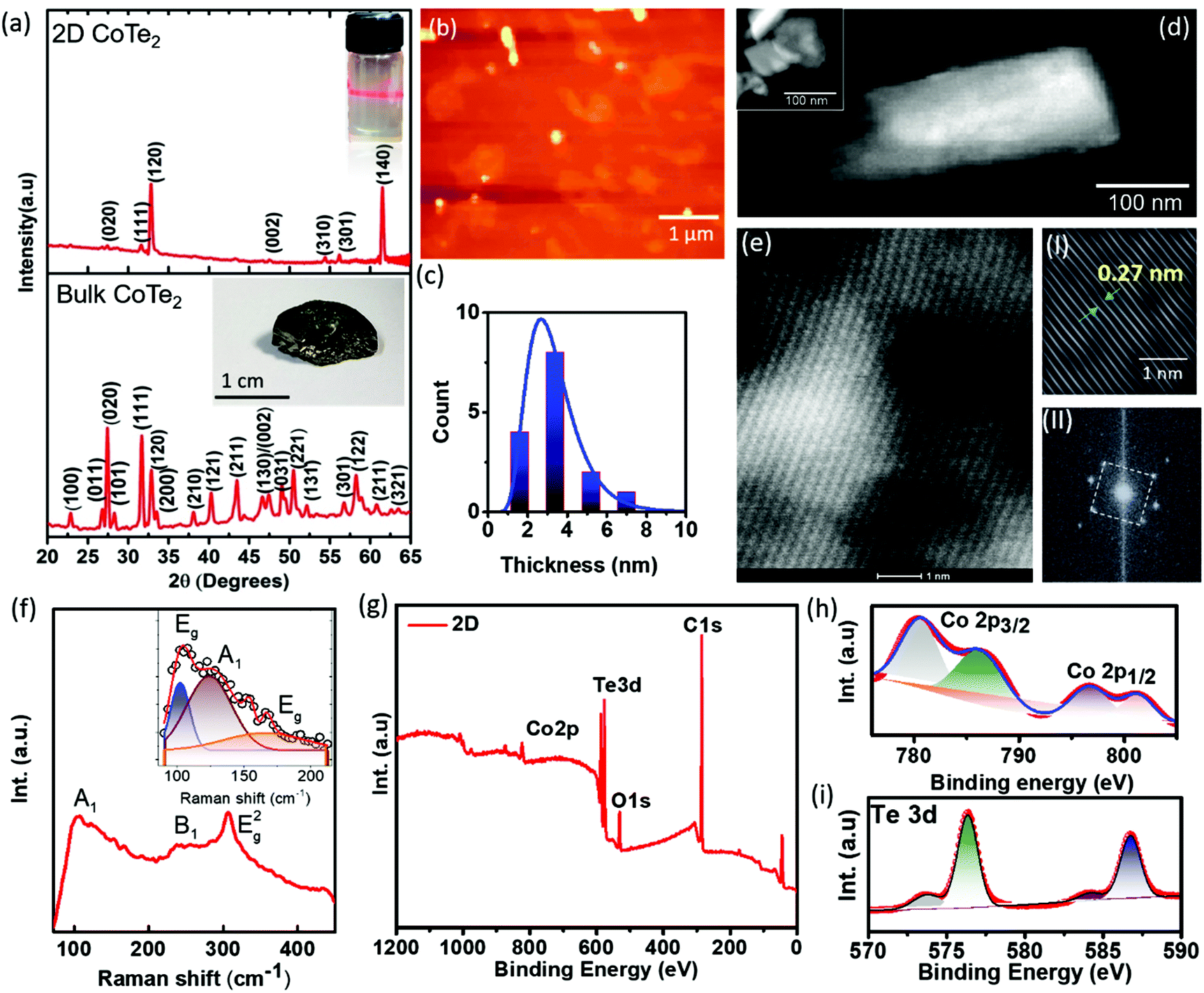 | ||
| Fig. 2 (a) The XRD patterns of bulk and 2D CoTe2. The digital images show bulk CoTe2 (lower inset) and dispersion of exfoliated CoTe2 in IPA solvent (upper inset). (b) AFM image of 2D CoTe2. (c) Histogram plot as a function of thickness. (d) Bright-field TEM image of exfoliated CoTe2 with a single layer shown in the inset. (e) HRTEM image of the exfoliated sample. (I) The upper inset shows the lattice fringe of 2D CoTe2. (II) The lower inset shows the FFT pattern. (f) The Raman spectrum of 2D CoTe2. (g) Full scan XPS spectra of exfoliated CoTe2. (h) De-convoluted XPS spectra of Co 2p. (i) Te 3d peaks. | ||
To clearly explore the semiconducting nature of the exfoliated sample, we measured the UV-vis absorption spectra with different size variations and it shows a clear absorption band in the UV (∼360 nm) and infrared regions (∼900–1050 nm) (Fig. 3a). The optical absorption results show a clear change in the absorption spectra as the size is decreased to a few nanometers, and the IR absorption decreased systematically and became flat. Fig. 3b shows the intensity ratio between the IR and UV bands as a function of particle size. It reveals the opening of the bandgap in the exfoliated samples when the dimensions of the material are reduced (d ≤ 4 nm). As the effective thickness approaches a few nanometers, more high-energy photons are absorbed than low-energy ones. This has also been reported in many studies where the material shows metallic behavior in bulk and a semiconductor one at nanosize.33 In Fig. 3c, we present the calculations for the infinite system to confirm that it is metallic but changes to a semiconductor one when the size of its corresponding finite flakes is decreased. We verified this by calculating the molecular orbitals of the systems with three different sizes: 36, 144, and, 324 atoms, respectively, as shown in Fig. 3c. We can see that the systems with 144 and 324 atoms are already metallic within DFT precision, while the one with 36 atoms exhibits a LUMO–HOMO difference (which can be associated with the bandgap) of about ∼0.13 eV. In Fig. S4a and b,† we present the optimized structure of the 2D CoTe2 unit cell, which contains 6 atoms (4Te + 2Co). The corresponding lattice parameters were obtained with the SIESTA (and Quantum Espresso) code corresponding to an orthorhombic unit cell with lattice vectors given by 3.03 and 8.07 Å along the X and Y directions, respectively. We observed five different bond length values: 2.45 and 2.66 Å for Co–Te, 2.98 and 3.17 Å for Te–Te and, 2.90 Å for Co–Co. Thus, there are two different bond types for Co–Te and Te–Te. In Fig. S4c and d,† we present the electronic band structure of layered CoTe2 and the corresponding projected density of states (PDOS) for the optimized structure shown in Fig. S4a and b.† It shows the metallic characteristics where the weight of the 3d atomic orbital is higher than those of others. We also investigated the effects of Co and Te vacancies and the system maintains its metallic behavior. Our simulations included spin polarization effects, and we verified that the system has an antiferromagnetic characteristic because the energy difference between the ferro and anti-ferro configurations is positive,
| ΔE = Eferromagnetic = Eanti-ferromagnetic = 0.4 eV | (1) |
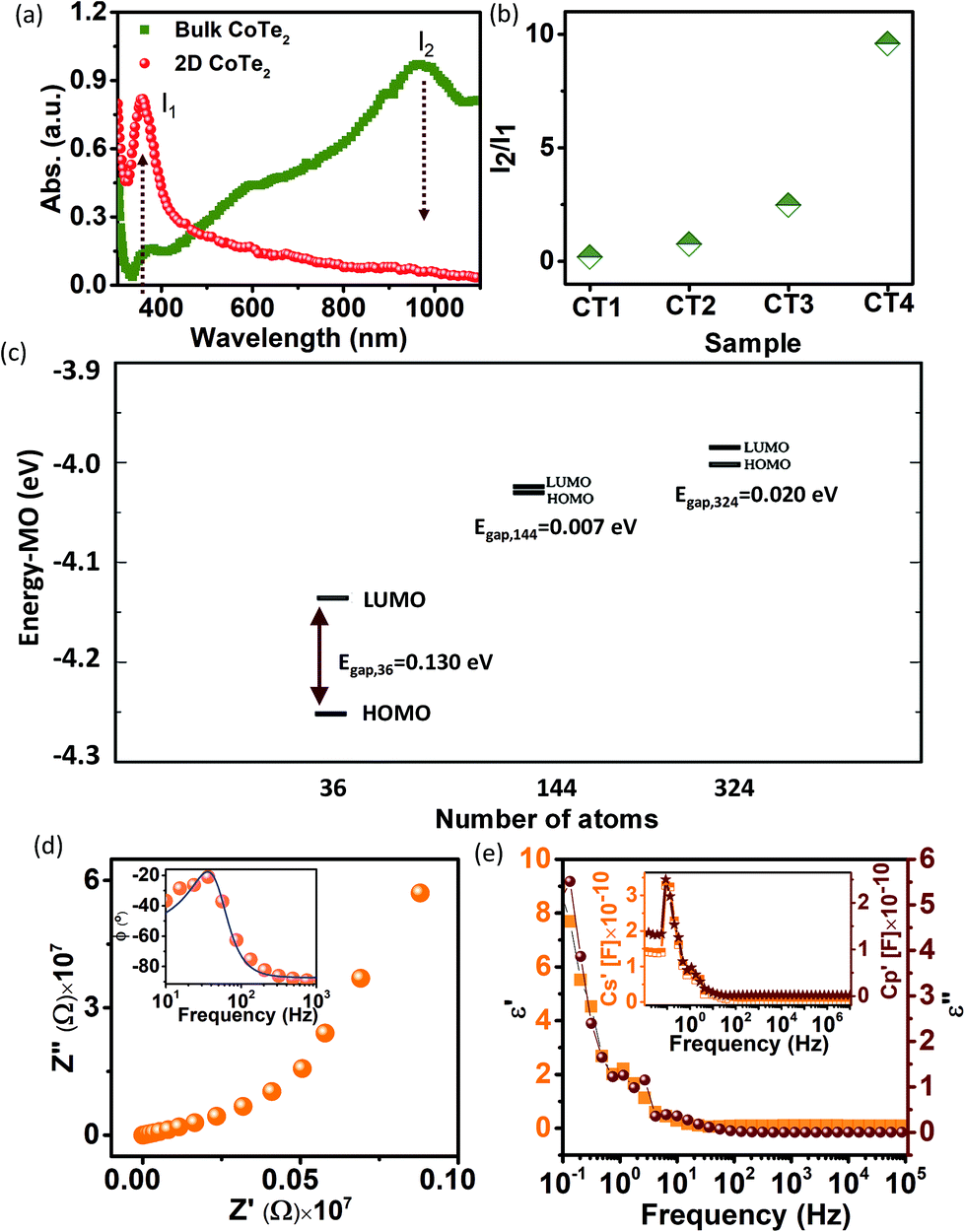 | ||
| Fig. 3 (a) UV-vis absorption spectra of bulk and 2D CoTe2 samples. (b) Intensity ratio of the IR band and UV band as a function of particle size. The size distribution of the synthesized samples is CT1 > CT2 > CT3 > CT4. Here, CT1 = bulk sample and CT4 = 2D CoTe2 with very small dimensions. (c) The molecular orbital values as a function of the number of atoms. The HOMO and LUMO refer to the highest occupied and the lowest unoccupied molecular orbitals, respectively. (d) EIS plot of the sample. The inset shows the impedance at lower frequency. The inset shows the negative phase angle vs. frequency. (e) Material permittivity and the inset shows the specific capacitance of the sample as a function of frequency. | ||
Electrochemical impedance spectroscopy (EIS) was performed in order to observe the capacitive behavior of the material at different frequencies. In Fig. 3d, we plotted the negative real impedance (−Z′) vs. positive imaginary impedance (Z′′), as the Nyquist plot of CoTe2. The diagram indicates a very good capacitive nature. The absence of semi-circles and a 45° line reveals a near-zero interfacial impedance and excellent charge transfer capability. The internal resistance obtained from the intercept on the x-axis is only ∼3.21 Ω, manifesting the ultrafast charge conduction inside the electrode. Another important analysis derived from the EIS data is shown in the inset of Fig. 3d. Here we have plotted the negative phase angle vs. frequency. At a certain frequency, the larger the corresponding negative phase angle, the stronger the capacitance characteristic. To distinguish the capacitance and resistance of the device, 45° is the key boundary. For CoTe2, the corresponding negative phase angle appears at ∼120 Hz. Therefore, the exfoliated sample shows capacitive behavior which helps store the generated charge during applied strain. Most significantly, the material shows the permittivity as a function of frequency and it was found that at low frequency, the value of permittivity is ∼7 (Fig. 3e). Therefore, our material shows dielectric behavior, which helps in the generation of charge as a function of strain. Furthermore, we have plotted the specific capacitance as a function of frequency (inset of Fig. 3e). At low frequency, CoTe2 shows a high value of capacitance and it confirms the charge storage capacity of the sample. These results support that the synthesized ultrathin sample can be fruitfully used in energy harvesting applications.
The fabrication of a PTNG using ultrathin CoTe2 has been illustrated in the Experimental section and ESI.†Fig. 4a shows the output voltage as a function of a periodic force (F) of 1 N. The maximum output voltage reaches up to ∼5 V. We calculated the response time of the fabricated PTNG, and it was found to be ∼4 ms (Fig. 4b). The generated output voltage from the PTNG by the repetitive finger (index and middle fingers) press and release motion is shown in the inset of Fig. 4c. By increasing the applied pressure (different fingers), the device produced an output voltage of ∼0.56 V and it increased up to ∼1.6 V (Fig. 4c). This also shows the great flexibility and voltage produced for bending measurements (Fig. 4d). A linear increase in the output voltage was observed which was directly proportional to the bending angle. Additionally, a maximum voltage of ∼1.5 V for the cell was achieved when it was connected over a bridge rectifier to obtain a positive voltage cycle (Fig. S5a and b†). We also compared the output performance to those of bulk CoTe2 samples, and a ten-fold increment of the output voltage under a periodic force of 1 N (Fig. 4e) was observed. These results confirmed that the generated output voltage originated from the ultrathin CoTe2. To know the internal resistance (RL) of the PTNG, the output voltage was recorded as a function of external load resistance (KΩ to MΩ), as shown in Fig. 4f. It is observed that the PTNG has an internal resistance of ∼9 MΩ. The maximum output power density (Pmax), output electrical energy (Eelec), total input mechanical energy (Emech), and energy-conversion efficiency (η) were calculated to know the efficiency of the fabricated PTNG34 and the detailed calculations are given in the ESI.† A Pmax value of ∼2.56 mW m−2 was obtained for the PTNG at an RL of 9 MΩ. The Eelec value was calculated to be ∼4.3 × 10⁻⁸ J at a maximum output voltage of ∼5 V, whereas the Emech value for an applied force of 1 N was 5.24 × 10⁻⁷ J. Therefore, the maximum conversion efficiency of the PTNG was found to be ∼8.2%. The current density was measured under the application of 1 N load on the PTNG cell at RT and found to be ∼60 nA m−2 (as seen in Fig. S6†). The proposed flexible PTNG will also provide effective electrical energy for real-world applications such as powering a blue LED in a sustainable manner (Fig. S7†). The voltage outputs of the LED with minimum glow were due to the low current output as mentioned above. The fabricated PTNG can provide a sustainable voltage with a current to power the connected LEDs for a longer duration when connected in series.
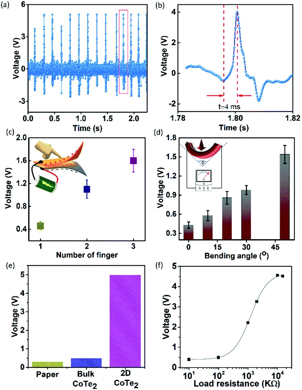 | ||
| Fig. 4 (a) The output voltage of the as-fabricated cell. (b) Enlarged view of a single pulse. (c) Output of the open-circuit voltage as a function of applied pressure for different finger pressures. The inset shows the schematic diagram of voltage generation using finger press as a pressure source. (d) Output voltage responses for different bending angles. The inset shows the schematic diagram of the bending measurement with a voltmeter. (e) The values of the output voltage of the fabricated cells. (f) The output voltage of the PTNG under different external load resistances varying from KΩ to MΩ. | ||
In order to investigate the elastic properties of ultrathin CoTe2, we replicated the unit cell of 2 × 2 × 1 along with the X and Y directions, building one orthorhombic supercell composed of 36 atoms. In Fig. 5a, we present the stress–strain curve for ultrathin CoTe2. We observed a significant anisotropy for the X and Y directions (see also Fig. 5b). The Young's modulus was calculated considering the linear regime for the strain value until 1%. The estimated Young's modulus values (from the linear regime of the stress/strain curve) were 163.73 and 72.13 GPa for the X and Y directions, respectively. We also analyzed the charge distortion effects in the elastic regime to obtain the piezoelectric coefficients using the expression:
| dijl = Pi/σjl, | (2) |
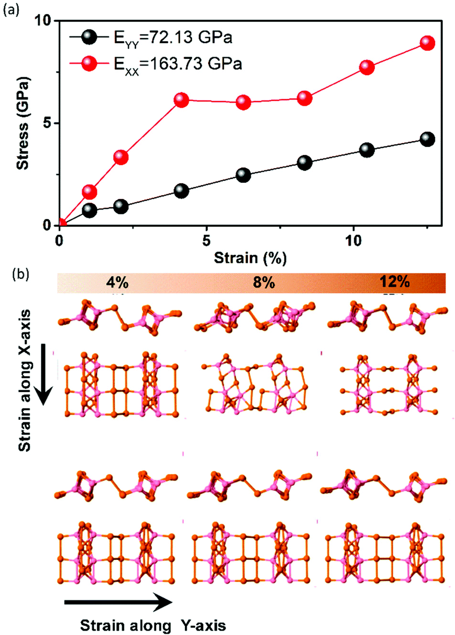 | ||
| Fig. 5 (a) Stress–strain curves of 2D CoTe2 considering one supercell composed of 36 atoms. The Young's modulus values for each direction are 163.73 and 72.13 GPa along the X and Y directions, respectively. (b) Deformation of the lattice structure along the X and Y axes as a function of applied strain. | ||
The charge generation mechanism of the PTNG under external stress is shown in Fig. S8 (a and b†), which is based on the piezoelectricity generated by ultrathin CoTe2 and the triboelectricity produced from the contact electrification process between Kapton and electrode materials (as discussed above, the dielectric properties of 2D CoTe2).We have schematically presented the working principle of the as-fabricated PTNG. In order to explain the voltage generation mechanism for the exfoliated CoTe2 based PTNG, we used a similar theoretical model to that reported by Yousry et al.35 Fig. S8a (aI and II)† shows the piezoelectric model, wherein mechanical stress is applied on the material with a non-centrosymmetric nature, and the centers of the positive and negative charges shift, which is also confirmed from DFT calculations, as discussed above. The charges generally move from one electrode to another until a point is reached where the potential difference between the electrodes is in a balanced (equilibrium) condition (Fig. S8a (I and II)†). The pressing action leads to stretching in the device, creating a piezoelectric polarization. The piezoelectric effect decreases when the external force is released, and the electrons flow back to the top and neutralize the positive potential. When the two surfaces are not in full contact, the triboelectric effect becomes prominent and produces a substantial electrical output (Fig. S8a (III)†). Simultaneously, as a result of this, polarization-free charges flow through the external circuit, maintaining the balance in the potential. Therefore, when an external pressure is applied, the dipole momentum and overall polarization in the pressed state are changed from the initial state; thus an electric current (IP) is generated as a response to the induced applied pressure (Fig. S8 (IV and V)†). After that, when the pressure is released, the opposite electrical potential change is induced, and the structure returns to its original state due to the triboelectric effect. We further analyzed the contribution of piezo and triboelectric modes in our PTNG. In Fig. S8(b),† we present the output performance of the triboelectric, piezoelectric, and hybrid energy harvesters under the same experimental conditions. The fabricated nanogenerator shows a maximum open-circuit voltage output of ∼2.4 V in triboelectric mode while it exhibits a voltage output of ∼0.6 V in piezoelectric mode, both under finger tapping conditions. However, for the hybrid PTNG device, the maximum open-circuit voltage output can reach up to ∼4 V (finger tapping), taking advantage of the synergistic combination of the two effects, which was much higher than the individual piezoelectric and triboelectric outputs. The output electrical potential depends on the deformation of the lattice structure of CoTe2, and it is due to the applied stress, as charges appear on the opposite faces in the material. The generated charges flow through the contact process between electrodes. The exfoliated CoTe2 suffices as a dielectric material in the contact process, which helps in charge transfer. Appropriate connections of the external electric circuit can generate an enhanced and reversible output signal with the electrons moving in the same direction. We also verified that the layer-dependent charge generation effect based on the Mulliken population is negligible, as shown in Fig. S9 in the ESI.† The durability demonstrated for the fabricated device under constant repetitive pressure showed stable behavior over a prolonged period (Fig. S10†). A fatigue test was carried out for the fabricated PTNG. The cell response is continuous and was studied for up to 200 cycles as seen in Fig. S11.† We observed that there is a drop in voltage from ∼5 V to ∼4.4 V, which indicates the good stability of the device. Using first-principles calculations, the piezo-coefficient of 2D CoTe2 is found to be 12.19 pm V−1. Compared to previous reports (see Fig. S12†), 2D CoTe2 produces a significant output response.
Telluride-based structures are widely researched for their thermoelectric behavior. Therefore, ultrathin CoTe2 can also be used as an energy harvesting device from different thermal sources. The utilization of waste heat dissipated for the generation of energy can account for waste heat management. Here we have measured the temperature-dependent behavior of 2D CoTe2. The temperature of the fabricated device was monitored using a laser thermometer. Meanwhile, the device output voltage at each changing temperature was recorded using a digital oscilloscope. With the slightest increase in temperature (in the range from 304 K to 373 K), the output voltage linearly increased (Fig. 6a) and then reached saturation. After the removal of the heat source, the maximum voltage attained is reduced to a minimum gradually. Fig. 6b shows the average values of the output voltage at increasing and decreasing temperatures. It was observed that the output voltage increased almost linearly and is directly proportional to the temperature change (Fig. 6c). The variation of the polarization of surface charges on the application of heat tends to generate significant thermionic vibrations; these vibrations are responsible for producing a drastic variation in the voltage. These produced charges are, in turn, responsible for the temperature-dependent piezoelectric effect that is observed in 2D CoTe2. An open-circuit voltage of ∼10 V was obtained from the PTNG, under a temperature variation from 305 K up to 363 K. We calculated the variation of output electrical energy for increased temperature values at a constant input mechanical energy of ∼5.24 × 10⁻⁷ J. It was observed that for the temperature increase from 305 K to 320 K, there was a gradual increase in efficiency (Fig. 6d and Table S1†). After that, the rate of efficiency increase tempered down. The CoTe2 based PTNG device shows a four-fold increment in conversion efficiency at the maximum temperature compared to RT. To confirm the temperature-induced strain in the atomically thin CoTe2, laser power-dependent Raman measurements were performed. It shows gradual shifting with increasing temperature (Fig. S13†). The temperature induced strain changes the lattice structure by absorbing the heat that creates surface charge and increases the output voltage. We would like to stress that, although the XPS results indicate the presence of Te–O bonds formed on the sample surfaces, these bonds are not very stable and break and/or dissociate under thermal treatments; thus the resulting surfaces are oxide-free. Theoretical studies were also performed in the same temperature region to analyze the origin of the higher energy conversion efficiency of the PTNG cell, discussed later. Therefore, this temperature range was feasible for low-grade-temperature device operation under non-ambient conditions, indicating internal overheating issues.
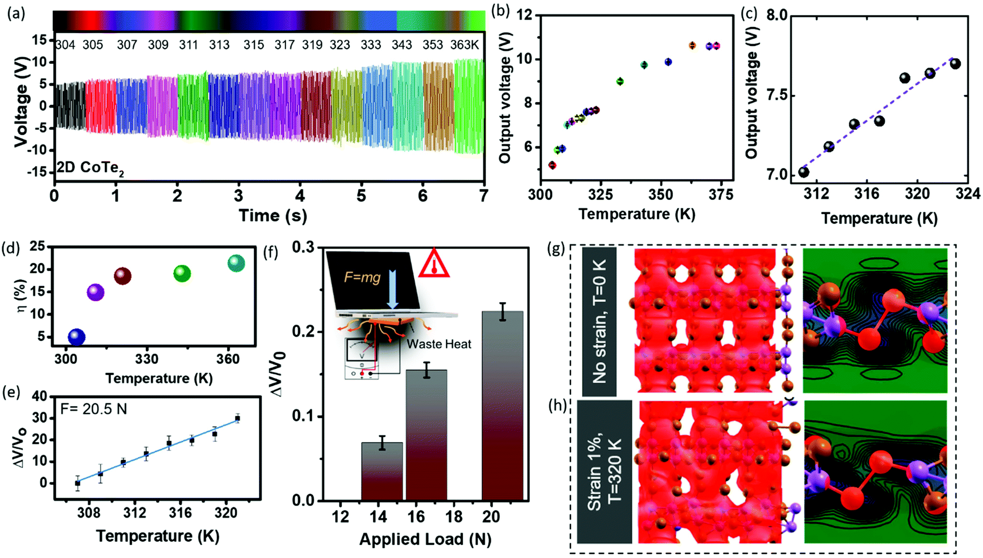 | ||
| Fig. 6 (a) Open-circuit voltage response as a function of temperature. (b) Variation of the average output voltage of the cell at different temperatures (increasing and decreasing) under a constant load. (c) Linear fitted curve of output voltage vs. temperature. (d) Energy conversion efficiency as a function temperature. (e) Relative voltage changes of the CoTe2 cell at various temperatures, with a sensitivity of 2.013 K−1 (room temperature up to 321 K). (f) Relative voltage changes of the cell as a function of the applied load. The inset shows the schematic illustration of the temperature measurement and sensing the temperature of a laptop. The electron density plot at the left from the top view and an isosurface value of 0.16 e Å−3 and an electron density map at the right from the side view at (g) 0 K, no strain, and (h) 320 K, 1% strain. | ||
The electronic devices used in our day-to-day activities radiate temperatures in the range of ∼300 K–325 K on constant usage. One such example is a laptop; we demonstrate that energy can be harvested from overheating of these devices. The average operating temperature of a laptop is below 313 K and above this temperature, internal problems of the device appear. In order to harness this energy, the fabricated PTNG was attached under a laptop (keyboard and touchpad), where most of the heat flow (overheating) is obtained during the working condition. To evaluate the performance of the fabricated PTNG cell, the generated output voltage was measured directly during the working condition of the laptop, as shown in the inset of Fig. 6f. The possibility to harvest waste-heat energy dissipated from the laptop by installing the described system on the source device was demonstrated successfully. The PTNG shows increased output voltage as a function of laptop temperature. A linear change is observed in the generated relative output voltage (ΔV/V0), with respect to increasing temperature (Fig. 6e). This indicates the generation of voltage in the PTNG cell, which is due to the temperature-dependent piezoelectric effect under the given experimental conditions. The responsivity (RS) (measurement of the input–output gain of a detector system) of a device is also a key parameter, and it was calculated using, Rs = (ΔV/V0)/T, where V0 is the initial output voltage at RT, and ΔV is the voltage change at temperature T. It is clearly noted that the device was responsive to temperature variations and exhibited a positive linear relationship in the temperature range of RT to 321 K with a response of 2.013 K−1. Therefore, the results confirm the application of our PTNG cell in scavenging waste heat dissipated during overheating of a laptop. Bulk materials generally harness large amounts of heat and temperatures; usually, small amounts of heat dissipated go unnoticed. Furthermore, the fabricated device was also sensitive as a function of laptop weight despite being a temperature sensing unit. Here, we have taken a different laptop and monitored their output voltage as a function of weight and heat generation (Fig. 6f). The calculated responsivity as a function of applied load (F = mg and m = weight of the laptop) also shows a linear behavior. Therefore, the fabricated lightweight and highly-sensitive PTNG cell can be used for monitoring the temperature of electronic gadgets.
The coupling of the piezoelectric and triboelectric properties of CoTe2 creates a polarized electric field with charge separations observed in a few layers of 2D CoTe2, which is a result of the time-dependent change in temperature.6,36 To explore the possible origin of this output voltage, we have used theoretical calculations on the application of strain and temperature. In Fig. 6g and h, we present the 3D electron density plot (upper) from a top view and the electron density map (lower) from a side view. For a small strain of 1% within the linear regime and a temperature of 320 K, we observed the charge distortion responsible for the changes in the electrical dipole value. In Table 1 we present the piezoelectric coefficients considering the linear elastic regime for a strain value of 1%. The results were obtained using optimized geometries from DFT calculations at T = 0 K and ab initio molecular dynamics for finite temperatures. We observed the same trend for the piezoelectric coefficient discussed in the present manuscript only for stress along the X-direction, as seen in Table 1. These cases occur as the coefficient values change when the temperature increases. With these above coefficients, we were further able to calculate the current density for various temperature conditions (details in the ESI†).37 Therefore, the current density (Isc) was calculated, and maximum current densities of ∼51 nA m−2 for 300 K and ∼67 nA m−2 for 320 K were obtained. The above theoretical simulation is consistent with experimental observation.
| Coefficients (pc N−1) | T = 0 K | T = 300 K | T = 320 K |
|---|---|---|---|
| d 11 (x) | −0.62 | 7.32 | 8.64 |
| d 12 | −4.75 | 57.8 | 41.3 |
| d 21 | −7.12 | 82.3 | 31.5 |
| d 22 (y) | 3.31 | 17.05 | 19.99 |
We would like to remark that while our theoretical results for infinite 2D CoTe2 shows metallic behavior, the experimental data show a semiconductor one after size reduction. The experimental samples considered in the manuscript are very small, because of the quantum confinement effects, and we can expect a transition from a metal to a semiconductor when the system size is decreased, and this is observed in our calculations (see Fig. 3c). The structural models in Fig. 3c did not consider defects and/or strain effects, and both contribute towards increasing the bandgap opening. Eqn (2) that we used to obtain the piezoelectric coefficients is valid only for semiconductors. The piezoelectric coefficients calculated along the X and Y directions for the system composed of 36 atoms are presented in Table 1. Interestingly, some coefficients are negative, but no clear pattern as a function of temperature is observed. This behavior has been also observed for other cobalt telluride families. We presented the results for the infinite system only to obtain some insights into the charge variation induced by the strain regime.
4. Conclusions
In conclusion, we could demonstrate a high-performance and flexible piezo-triboelectric nanogenerator using 2D CoTe2 as an active material. This device was used as a mechanical energy harvesting unit, and it also acts as a self-powered nanogenerator. 2D CoTe2 samples were prepared by a liquid exfoliation method, and their piezo-triboelectric properties were systematically studied. The experimental results demonstrate that the piezo and triboelectric performance of the exfoliated CoTe2 shows an exemplary output voltage. The hybrid nanogenerator can generate up to 5 V by applying a periodic force of 1 N. Also, the temperature-dependent behavior of the output performance of the PTNG cell was investigated. The PTNG shows high-temperature stability in the range of 305 K–363 K with an output voltage of ∼10 V with a four-fold enhancement in energy conversion efficiency which was achieved at the maximum temperature. The relative voltage (V/V0) changed from ∼0.085 V to ∼0.225 V as the laptop weight increased and with the increase in waste heat dissipation, a high responsivity of 2.013 K−1 was noted. To explore the possible origin of this output voltage we used DFT calculations in combination with the application of strain and temperature. Therefore, we believe that our work provides a framework for increasing the output power of conventional power generators and will pave the way for the realization of self-powered energy systems such as mobile electronic devices and energy harvesting approaches that use 2D materials from various thermal sources and dissipate waste heat from electronic devices.Author contributions
Solomon Demiss Negedu: data curation, formal analysis, and writing – original draft; Raphael Tromer: software; Chinmayee Chowde Gowda: formal analysis and writing – review and editing; Cristiano F. Woellner: software; Femi Emmanuel Olu: validation, methodology and writing-review and editing; Ajit K. Roy: validation, writing-review and editing; Prafull Pandey: data curation and methodology; Douglas S. Galvao: visualization, writing – review and editing, and supervision; Pulickel M. Ajayan: supervision; Partha Kumbhakar: conceptualization and writing – review and editing; and Chandra S. Tiwary: visualization, funding acquisition, supervision, and writing – review and editing.Conflicts of interest
There are no conflicts to declare.Acknowledgements
P. K. and C. S. T. acknowledges AOARD (Asian Office of Aerospace Research and Development) grant no. FA2386-19-1-4039. C. S. T. acknowledges Ramanujan fellowship and core research grant of SERB, India. CST acknowledges the funding received from STARS project by MHRD, India.References
- Y. Liua and C. Hu, Nanoscale, 2020, 12, 20118–20130 RSC.
- F. Yi, H. Ren, J. Shan, X. Sun, D. Wei and Z. Liu, Chem. Soc. Rev., 2018, 47, 3152–3188 RSC.
- H. Khan, N. Mahmood, A. Zavabeti, A. Elbourne, M. A. Rahman, B. Y. Zhang, V. Krishnamurthi, P. Atkin, M. B. Ghasemian, J. Yang, G. Zheng, A. R. Ravindran, S. Walia, L. Wang, S. P. Russo, T. Daeneke, Y. Li and K. Kalantar-Zadeh, Nat. Commun., 2020, 11, 1–8 CrossRef PubMed.
- Y. Yang, W. Guo, K. C. Pradel, G. Zhu, Y. Zhou, Y. Zhang, Y. Hu, L. Lin and Z. L. Wang, Nano Lett., 2012, 12, 2833–2838 CrossRef CAS PubMed.
- J. Jung, H. Cho, R. Yuksel, D. Kim, H. Lee, J. Kwon, P. Lee, J. Yeo, S. Hong, H. E. Unalan, S. Han and S. H. Ko, Nanoscale, 2019, 11, 20356–20378 RSC.
- C. X. Lu, C. B. Han, G. Q. Gu, J. Chen, Z. W. Yang, T. Jiang, C. He and Z. L. Wang, Adv. Eng. Mater., 2017, 19, 1–8 CAS.
- M. B. Ghasemian, T. Daeneke, Z. Shahrbabaki, J. Yang and K. K. Zadeh, Nanoscale, 2020, 12, 2875–2901 RSC.
- A. L. Cottrill, A. T. Liu, Y. Kunai, V. B. Koman, A. Kaplan, S. G. Mahajan, P. Liu, A. R. Toland and M. S. Strano, Nat. Commun., 2018, 9, 1–11 CrossRef CAS PubMed.
- P. Liu, A. T. Liu, D. Kozawa, J. Dong, J. F. Yang, V. B. Koman, M. Saccone, S. Wang, Y. Son, M. H. Wong and M. S. Strano, Nat. Mater., 2018, 17, 1005–1012 CrossRef CAS PubMed.
- Z. Liu, H. Li, B. Shi, Y. Fan, Z. L. Wang and Z. Li, Adv. Funct. Mater., 2019, 29, 1–19 Search PubMed.
- K. I. Park, S. B. Bae, S. H. Yang, H. I. Lee, K. Lee and S. J. Lee, Nanoscale, 2014, 6, 8962–8968 RSC.
- T. Zhang, T. Yang, M. Zhang, C. R. Bowen and Y. Yang, iScience, 2020, 23, 101689 CrossRef CAS PubMed.
- L. Lapčinskis, K. Mālnieks, A. Linarts, J. Blūms, K. N. Šmits, M. Järvekülg, M. R. Knite and A. Šutka, ACS Appl. Energy Mater., 2019, 2, 4027–4032 CrossRef.
- S. Karmakar, P. Kumbhakar, K. Maity, D. Mandal and P. Kumbhakar, Nano Energy, 2019, 63, 103831 CrossRef CAS.
- W. Chen, X. Hou, X. Shi and H. Pan, ACS Appl. Mater. Interfaces, 2018, 10, 35289–35295 CrossRef CAS PubMed.
- X. Song, F. Hui, T. Knobloch, B. Wang, Z. Fan, T. Grasser, X. Jing, Y. Shi and M. Lanza, Appl. Phys. Lett., 2017, 111, 083107 CrossRef.
- L. Dong, J. Lou and V. B. Shenoy, ACS Nano, 2017, 11, 8242–8248 CrossRef CAS PubMed.
- M. Chhowalla, H. S. Shin, G. Eda, L. J. Li, K. P. Loh and H. Zhang, Nat. Chem., 2013, 5, 263–275 CrossRef PubMed.
- R. Fei, W. Li, J. Li and L. Yang, Appl. Phys. Lett., 2015, 107, 173104 CrossRef.
- H. Fang, Z. Luo, H. Yang and Y. Wu, Nano Lett., 2014, 14, 1153–1157 CrossRef CAS PubMed.
- R. Hinchet, U. Khan, C. Falconi and S. W. Kim, Mater. Today, 2018, 21, 611–630 CrossRef CAS.
- C. Cui, F. Xue, W. J. Hu and L. J. Li, npj 2D Mater. Appl., 2018, 2, 18 CrossRef.
- Y. Wang, N. Xu, D. Li and J. Zhu, Adv. Funct. Mater., 2017, 27, 1604134 CrossRef.
- A. Apte, S. Kouser, F. Safi Samghabadi, L. Chang, L. M. Sassi, D. Litvinov, B. I. Yakobson, A. B. Puthirath and P. M. Ajayan, Mater. Today, 2021, 44, 40–47 CrossRef CAS.
- K. A. N. Duerloo, M. T. Ong and E. J. Reed, J. Phys. Chem. Lett., 2012, 3, 2871–2876 CrossRef CAS.
- H. Ma, W. Dang, X. Yang, B. Li, Z. Zhang, P. Chen, Y. Liu, Z. Wan, Q. Qian, J. Luo, K. Zang, X. Duan and X. Duan, Chem. Mater., 2018, 30, 8891–8896 CrossRef CAS.
- T. H. Lu, C. J. Chen, M. Basu, C. G. Ma and R. S. Liu, Chem. Commun., 2015, 51, 17012–17015 RSC.
- X. Wang, Z. Zhou, P. Zhang, S. Zhang, Y. Ma, W. Yang, H. Wang, B. Li, L. Meng, H. Jiang, S. Cui, P. Zhai, J. Xiao, W. Liu, X. Zou, L. Bao and Y. Gong, Chem. Mater., 2020, 32, 2321–2329 CrossRef CAS.
- Q. Wang, K. Cui, J. Li, Y. Wu, Y. Yang, X. Zhou, G. Ma, Z. Yang, Z. Lei and S. Ren, Nanoscale, 2020, 12, 9171–9177 RSC.
- M. Yamamoto, S. T. Wang, M. Ni, Y. F. Lin, S. L. Li, S. Aikawa, W. B. Jian, K. Ueno, K. Wakabayashi and K. Tsukagoshi, ACS Nano, 2014, 8, 3895–3903 CrossRef CAS PubMed.
- X. Chia, Z. Sofer, J. Luxa and M. Pumera, Chem. – Eur. J., 2017, 23, 11719–11726 CrossRef CAS PubMed.
- X. Wang, X. Huang, W. Gao, Y. Tang, P. Jiang, K. Lan, R. Yang, B. Wang and R. Li, J. Mater. Chem. A, 2018, 6, 3684–3691 RSC.
- A. Vargas, S. Basak, F. Liu, B. Wang, E. Panaitescu, H. Lin, R. Markiewicz, A. Bansil and S. Kar, ACS Nano, 2014, 8, 1222–1230 CrossRef CAS PubMed.
- K. Maity, S. Garain, K. Henkel, D. Schmeißer and D. Mandal, ACS Appl. Polym. Mater., 2020, 2, 862–878 CrossRef.
- Y. M. Yousry, K. Yao, A. M. Mohamed, W. H. Liew, S. Chen and S. Ramakrishna, Adv. Funct. Mater., 2020, 30, 1–9 CrossRef.
- C. R. Bowen, J. Taylor, E. Leboulbar, D. Zabek, A. Chauhan and R. Vaish, Energy Environ. Sci., 2014, 7, 3836–3856 RSC.
- S. K. Ghosh, P. Adhikary, S. Jana, A. Biswas, V. Sencadas, S. D. Gupta, B. Tudu and D. Mandal, Nano Energy, 2017, 36, 166–175 CrossRef CAS.
Footnotes |
| † Electronic supplementary information (ESI) available. See DOI: https://doi.org/10.1039/d2nr00132b |
| ‡ These authors contributed equally to this work. |
| This journal is © The Royal Society of Chemistry 2022 |