
 Open Access Article
 This Open Access Article is licensed under a
 Creative Commons Attribution 3.0 Unported Licence
Doping MAPbBr3 hybrid perovskites with CdSe/CdZnS quantum dots: from emissive thin films to hybrid single-photon sources†
Justine
Baronnier
,
Julien
Houel
 *,
Christophe
Dujardin
,
Florian
Kulzer
* and
Benoît
Mahler
*
*,
Christophe
Dujardin
,
Florian
Kulzer
* and
Benoît
Mahler
*
Institut Lumière Matière, UMR5306 Université Lyon 1-CNRS, Université de Lyon, 69622 Villeurbanne cedex, France. E-mail: julien.houel@univ-lyon1.fr; benoit.mahler@univ-lyon1.fr; florian.kulzer@univ-lyon1.fr
First published on 23rd March 2022
Abstract
We report the first doping of crystalline methyl–ammonium lead bromide perovskite (MAPbBr3) films with CdSe/CdZnS core/shell quantum dots (QDs), using a soft-chemistry approach that preserves their high quantum yield and other remarkable luminescence properties. Our approach produces MAPbBr3 films of around 100 nm thickness, doped at volume ratios between 0.01 and 1% with colloidal CdSe/CdZnS QDs whose organic ligands were exchanged with halide ions to allow for close contact between the QDs and the perovskite matrix. Ensemble photoluminescence (PL) measurements demonstrate the retained emission of the QDs after incorporation into the MAPbBr3 matrix. Photoluminescence excitation (PLE) spectra exhibit signatures of wavelength-dependent coupling between the CdSe/CdZnS QDs and the MAPbBr3 matrix, i.e., a transfer of charges from matrix to QD, which increases the QD luminescence by up to 150%, or from QD to matrix. Spatially-resolved PL experiments reveal a strong correlation between the positions of QDs and an enhancement of the PL signal of the matrix. Lifetime imaging of the doped films furthermore shows that the emission lifetime of MAPbBr3 is slower in the vicinity of QDs, which, in combination with the increased PL signal of the matrix, suggests that QDs can act as local nucleation seeds that improve the crystallinity of MAPbBr3, thus boosting its emission quantum yield. Luminescence antibunching measurements provide clear evidence of single-photon emission from individual QDs in perovskite. Finally, the analysis of blinking statistics indicates an improvement of the photostability of individual QDs in perovskite as compared to bare CdSe/CdZnS QDs. At high CdSe/CdZnS QD doping levels, this work thus opens a route to hybrid solar concentrators for visible-light harvesting and hybrid-based LEDs, while a low degree of doping could yield hybrid single-photon sources than can be embedded in field-effect devices for single-charge control, which would allow the construction of nanophotonic devices via low-cost solution-processing techniques as an alternative to solid-state quantum dots.
1 Introduction
Research on hybrid perovskites for photovoltaics has been booming since 2009, evolving from the first reported efficiency of 3.8% for a solar cell using perovskites as photo-active materials1 to an efficiency of 25% in 2021.2 Since then, the literature and potential applications of hybrid perovskites have grown exponentially.3–6 In addition to their remarkable optical and transport properties, this success of hybrid halide perovskites is explained by them being easy to process and allowing the creation of multi-scale compounds (from bulk7 to thin-films8 and quantum dots (QDs)9), as well as by their compatibility with industry-scale soft-chemistry processes.5,10 An important step in this direction was recently taken with the use of hybrid perovskites (methylammonium lead iodide, MAPI) to create a host matrix for a different active material (PbS QDs).11 However, this first QD-in-perovskite hybrid offers only limited perspectives for luminescence applications, on the one hand because PbS NCs emit in the infrared, which is not ideal for solar concentrators or LED applications and on the other hand because their low fluorescence quantum yield (QY) has so far not allowed the observation of single nano-objects, which would be essential for potential applications as single-photon sources (SPS). Following that first milestone, several promising ways to take advantage of the properties of II–VI QDs and hybrid perovskites have been proposed: a thin film containing CdSe and CsPbI3 QDs has been deposited on top of MAPbI3 to study potential increases in conversion efficiency of perovskite-based solar cells.12 PbSe nanowires have been coated with CsPbBr3 for applications as photodetectors.13 CsPbBr3/CdS core/shell QDs with enhanced stability have been synthesized.14 Another recent example is the creation of CsPbBr3/ZnS heterodimers and heterostructures to enhance stability.15 In spite of these important developments, no successful realization of visible-range QD-in-perovskite hybrid has been reported so far to the best of our knowledge. CdSe colloidal quantum dots (QDs) are an economical, easy-to-tune, highly fluorescent active material.16,17 The chemical synthesis of QDs is already established at the industrial scale and can be found in consumer products. Additional advantages of QDs are their tunable emission with nanosecond radiative recombination lifetimes and their tunable sheet density, which can be orders of magnitude higher than what is achievable by epitaxial growth. As a consequence, substantial research effort has been dedicated to CdSe QDs in LEDs,18 solar cells,19,20 solar concentrators21 or as SPS and building blocks for quantum-information devices.22–25 Unfortunately, the fragility of this class of emitters during encapsulation process26,27 and the lack of compatible semiconductor host matrices has rendered difficult their incorporation in crystalline, fast charge-transfer devices analog to what was achieved with state-of-the-art InGaAs diodes.28 The semiconductor nature of hybrid perovskites and the process compatibility between CdSe-QD synthesis and perovskite thin-film elaboration (soft chemistry) suggests that combining the remarkable properties of these two materials is an intrinsically interesting route for applications such as light converters (solar concentrator or LEDs at high doping level) and single photon sources (at low doping level). For the last two years, an intense effort has been put on coupling high quantum yield CdSe-based QDs with either organic or inorganic hybrid perovskite.3–5,12,29 So far, research has reported on either depositing CdSe QDs over a perovskite layer to enhance its light harvesting properties,29 or insertion of CdSe and CsPbI3 in between a MAPbI3 layer and a hole transport layer.12 However, to the best of our knowledge, none of the results reported so far was able to retain the fluorescence efficiency and single photon emission capability, which are actually the best assets of CdSe-based colloidal QDs.In this article, we present the first emissive QD-in-perovskite hybrids in the visible range, based on thin MAPbBr3 films doped with highly fluorescencent CdSe/CdZnS core/shell quantum dots. We present ensemble photoluminescence (PL) spectra demonstrating emission of these films at the CdSe/CdZnS wavelength. Photoluminescence excitation (PLE) experiments were performed, which demonstrate different types of coupling between the CdSe/CdZnS QDs and the MAPbBr3 matrix. The combination of confocal PL microscopy and fluorescence lifetime imaging (FLIM) reveal sub-micron-scale correlations between the emission of the QDs and the MAPbBr3 matrix. Finally, confocal PL microscopy demonstrates the first QD-in-perovskite hybrid single photon source emitting in the visible, with blinking properties enhanced compared to the non-encapsulated QDs.
2 Methods
2.1 Quantum dot synthesis
CdSe/Zn1−xCdxS colloidal quantum dots (CQDs) were synthesized following ref. 30 and 31. To create the CdSe core, 15 mL of octadecene (ODE), 1 mmol of cadmium oxide and 3 mmol of myristic acid were introduced in a three-neck flask. The mixture was degassed at 60 °C under vacuum for ten minutes before being heated to 300 °C under argon. When the mixture became transparent, 0.25 mL of TOPSe at 2 M in TOP was introduced to react at 300 °C for three minutes. The Zn1−xCdxS shell was then created: 3 mL of zinc oleate (Zn(OA)2) at 0.5 M in ODE and 1 mmol of dodecanthiol (DDT) were injected over the course of one minute. The solution was then left to react at 300 °C for 30 minutes; the nominal composition of the shell created in this first growth step was 60% of Cadmium and 20% of Zinc. 2 mL of cadmium oleate (Cd(OA)2) at 0.5 M in ODE, 4 mL of Zn(OA)2 at 0.5 M in ODE and 1.5 mL of TOPS at 2 M in TOP were subsequently injected in one minute. This mixture was heated during 10 minutes to 300 °C. This step was repeated 4 times, resulting in a compositional-gradient CdZnS shell. The final synthesized QDs were isolated by precipitation and centrifugation, then redispersed in 10 mL of hexane.2.2 Ligand exchange
An OA-to-halide ligand exchange was necessary to ensure solubility of the CQDs in N,N-Dimethylformamide (DMF), the solvent for the perovskite precursor. To this end, 60 μL of the previously-synthesized CQD solution were diluted in 2 mL of hexane and mixed with 1 mL of DMF solution containing methylammonium bromide (0.2 M) and cadmium bromide (0.3 mmol). This biphasic solution was stirred for three hours, at which point the CQDs were precipitated with isopropanol and redispersed in DMF two times. In the end, CQDs with bromide ligands were dispersed in DMF (2 mL) and 1 mL of methylammonium chloride (0.1 M), then the solution was sonicated for 25 minutes at 50 °C. Further details of this ligand-exchange procedure, as well as an exhaustive optical characterization of the obtained halide-covered CdSe/CdZnS CQDs, can be found in ref. 31.2.3 Perovskite thin films
Thin perovskite films were deposited on BK7 glass substrates using the antisolvent-injection method.32–34 The glass substrates were sonicated at 60 °C in a succession of a 0.5% aqueous solution of Triton X100, demineralized water, and isopropanol, with a rinsing step in demineralized water between each change of bath. After drying under vacuum for 10 minutes, the cleaned substrates were introduced in an argon-filled glovebox, where the deposition procedure was carried out. The perovskite precursor was prepared by dissolving appropriate quantities of methylammonium bromide MABr and lead bromide PbBr2 in DMF to obtain a 1 M solution of MAPbBr3. 100 μL of this precursor solution were deposited on a glass substrate at rest, which was then spun at 5000 rpm for 60 s; manual injection of the antisolvent, 1 mL of chlorobenzene, took place 5 s after the start of this spinning period.2.4 QD-in-perovskite heterostructures
Thin-film QD-in-perovskite heterostructures were created by spin-coating a solution of perovskite precursor and halide-ligand QDs onto a glass (BK7) slide: mixtures of 100 μL of perovskite precursor solution at 1 M and 100 μL of halide-capped QDs in DMF with varying concentrations were spin-cast at 5000 rpm for 60 seconds; 5 seconds after the start, 1 mL of chlorobenzene was injected. The nominal QD-doping percentages (volume/volume) reported in this article are based on the lead-to-cadmium stoichiometric ratios calculated from the concentrations of the components in the perovskite/QD precursor mix used to prepare a given hybrid film.2.5 Ensemble spectroscopy
An FS5 spectrofluorometer (Edinburgh Instruments) was used for ensemble spectroscopy. Absorption spectra were obtained by measuring the intensity transmitted by a given sample as a function of wavelength, followed by a baseline reference measurement of an empty substrate. Photoluminescence (PL) spectra were recorded with an excitation wavelength of 405 nm, an integration times of 300 ms per data point, and a spectral resolution of 1 nm. Photoluminescence-excitation spectra (PLE) used a detection wavelength of 645 nm, an integration time of 1 s per data point, and a spectral resolution of 1 nm.2.6 Spatially-resolved photoluminescence lifetime measurements
Spatially resolved lifetime measurements were performed with the home-built confocal microscope described in detail in ref. 35. Briefly, an oil-immersion objective (Olympus NA = 1.35, 60×) was used to both focus the pulsed excitation laser (Edinburgh Instruments EPL0450, emitting at 445 nm with repetition rate of 2 MHz) and collect the position-dependent emission while the sample was raster-scanned though the focus with a piezo positioner. Detection was assured by two single-photon avalanche photodiodes (SPADs), an ARQH-050 (PerkinElmer) for QD luminescence and a Count-20 C (Laser Components) for the MAPbBr3 signal; the outputs of these detectors were connected to a time-correlated single-photon counting card (TimeHarp 200 with router, PicoQuant). The spectral filters used for selective detection were a combination of an FBH650-40 bandpass (Thorlabs) with a BrightLine 655/15 bandpass (Semrock) for QD emission and a 532/10 bandpass (Edmund Optics, 65–700) with an OD = 1 neutral density filter for the MAPbBr3 signal. The confocal images presented in this article are the sums of 10 consecutive scans of the same sample area with 100 ms integration time per pixel per scan; a cross-correlation-based automatic correction was applied before summing the individual images to compensate for the small in-plane drift of less than 1 μm that occurred between each pair of consecutive images.2.7 Individual QDs in perovskite
Individual QDs were studied in the QD-in-perovskite hybrid films using the confocal microscope described above. Antibunching and blinking measurements were performed under continuous-wave laser excitation at 561 nm (Exelitas) and with a combination of bandpass filters (Thorlabs FBH650-40 and Semrock BrightLine 655/15) placed in front of both SPADs.3 Results and discussion
The discussion of our experimental results in this section is organized as follows: we first present the morphological and structural properties of pure perovskite films deposited with our approach, after which we focus on photoluminescence and photoluminescence-excitation spectra of QD-in-perovskite hybrid samples at different doping percentages; a model is proposed to explain the host–guest coupling phenomena that we observed. A discussion of the single-photon emission properties and the photostability of individual QDs in MAPbBr3 closes the section.3.1 Thin films of undoped perovskite
Fig. 1 gives an overview of the optical and structural properties of undoped MAPbBr3 films. As can be seen in Fig. 1a, the deposition protocol detailed in Methods yields centimeter-sized, transparent yellow/orange films without noticeable milkiness or any other signs of significant diffusion. The absorption spectrum exhibits a strong and narrow absorption peak at 520 nm typical of an MAPbBr3 exciton36 (Fig. 1a); the corresponding photoluminescence (PL) spectrum shows a narrow emission peak centered at 540 nm, with a full width at half-maximum (FWHM) of 35 nm. We note that the emission is actually structured by two peaks at λ = 533 and 544 nm, whose intensity ratio we found to be varying for different regions of the sample. The emission at 533 nm is attributed to the band-edge free exciton,37–39 and the emission at 544 nm to shallow defects near the MAPbBr3 band-edge.38,40 Although these shallow defects unambiguously contribute to the emission spectrum, they do not have a clear signature in the perovskite absorption spectrum, which points to a vanishing absorption coefficient and suggests that their emission is activated via charge relaxation from the MAPbBr3 band-edge exciton.38,39 | ||
| Fig. 1 Optical and structural characterization of thin films of undoped MAPbBr3 on BK7. (a) Absorption (solid line) and PL emission spectrum (dashed, excitation wavelength 405 nm); the inset shows a white-light photograph with a reference grid (periodicity: 5 mm) placed underneath the glass substrate on which the film was deposited. (b) Height profile of a film measured by atomic force microscopy (AFM) on the edge of a crack on the sample surface shown in the microscopy image in the inset (scale bar: 100 μm; the arrow-shaped black feature is the shadow of the AFM cantilever). (c) Scanning electron microscopy (SEM) images of the film surface at two different magnifications (top and bottom panel); the scale bar indicates 5 μm in both cases. (d) X-ray diffraction diagram of a film in Bragg–Brentano geometry (top panel) and under grazing incidence (bottom panel), respectively; diffraction peaks have been labeled with the Miller indices of the corresponding lattice planes. | ||
Atomic force microscopy (AFM) revealed a thickness of around 150 nm for the undoped MAPbBr3 films deposited from the precursor solution at 1 M, as can be seen in Fig. 1b, which shows a topographic line profile along the edge of a crack on the sample surface presented in the optical microscope picture in the inset of the graph. The QD-doped hybrid films that will be discussed in the coming sections, on the other hand, were deposited from a 0.5 M perovskite precursor due to dilution by mixing with the solution containing the QDs; the average thickness of the doped films was therefore smaller, 88 ± 6 nm.
Fig. 1c shows a scanning electron microscopy (SEM) image of a 110 × 25 μm2 area of the perovskite surface (top panel), which appears homogeneous on this scale with occasional straight-line cracks. A magnified SEM picture covering a region of 11 × 2.5 μm2 (bottom panel) reveals a fine structure composed of sub-micron crystallites in an arrangement that suggests a compact thin film of MAPbBr3. The X-ray diffraction diagrams in Fig. 1d confirm that only (00x) lattice planes with x = 1, 2, 3 contribute in standard geometry (normal incidence), suggesting preferential orientation of the thin-film crystallites along those axes; under grazing incidence, on the other hand, additional diffraction peaks associated with other crystallographic planes are detected. We therefore conclude that the injection of the chlorobenzene antisolvent32–34 has indeed induced crystallization of the film without any annealing step being necessary after deposition, contrary to MAPI thin films.41
3.2 QD-in-perovskite hybrid: ensemble luminescence spectroscopy
Fig. 2a shows the photoluminescence (PL) spectra of four different QD-doped MAPbBr3 thin films, labeled samples A–D and doped at 0.025, 0.1, 0.5, and 1% (volume/volume), respectively, with CdSe/CdZnS QDs. All four spectra were normalized to the same integrated intensity of the perovskite emission band (500–580 nm) to facilitate comparison of the relative QD emission intensity (above 600 nm), which ranges from barely visible above the background (sample A) to more intense than the matrix emission (sample D). What is more, the relative QD intensity remained roughly proportional to the doping level as the latter was changed by a factor of 40, as can be seen in Fig. 2b: if the normalized PL spectra of the four samples are rescaled to take into account the differences in nominal doping percentage (taking sample B as the reference), then the heights of the QD emission bands become comparable, with very good agreement between the two low-concentration samples (A and B) and a deviation from proportionality of less than 30% for the two higher doping levels. The center of the QD emission band and its full width at half maximum (FWHM) remained unchanged at 638 nm and 43 nm respectively, for all doping levels considered here; we attribute this observed red-shift of the emission maximum of 4 nm (compared to bare QDs on BK7, see Fig. S1 and Table S1 in the ESI†) to the successful encapsulation of the QDs in the MAPbBr3 matrix, due to which the surrounding perovskite acts as an extended shell that modifies the potential barrier experienced by the QD exciton. The shape of the emission band, on the other hand, remained unchanged in all samples, suggesting good overall structural compatibility of the halide-capped QDs with the perovskite matrix. This interpretation is further supported by the fact that the X-ray diffractogram of the doped MAPbBr3 matrix is identical to that of undoped films, as well as by the homogeneous distribution of the QD photoluminescence over a macroscopic scale and by the photoluminescence survival after on-shelf storage under ambient conditions for a period of weeks to months. (These data are presented in section 2 of the ESI.†) | ||
| Fig. 2 Photoluminescence (PL) and photoluminescence excitation (PLE) spectra of perovskite (MAPbBr3) thin films doped with CdSe/CdZnS QDs. (a) PL spectra of four samples with doping levels (nominal volume/volume) ranging from 0.025% (sample A) to 1% (sample D). These spectra have been normalized with respect to the total area of the perovskite emission band (500–580 nm), and then the height of the narrowest peak (sample B) was chosen to define 1.0 on the y-axis; excitation wavelength: 405 nm. (b) The normalized PL spectra already shown in (a) after further rescaling according to their nominal doping levels compared to that of sample B: the spectrum of sample A was multiplied by four, while those of samples C and D were divided by five and ten, respectively. A PL spectrum of a film of bare QDs on glass, scaled to match the height of the band of sample B, is included for comparison. (c) Normalized PLE spectra S(λ) of samples A and B, detected at the maximum of QD emission (650 ± 1 nm). Both spectra were rescaled to the same average intensity (dotted horizontal line) in the spectral region above 550 nm (gray background), where perovskite absorption is negligible. The reference PLE spectrum Sref(λ) of bare QDs on glass was rescaled in the same manner and then furthermore corrected for perovskite absorption, which yields the expected PLE spectrum S0(λ) in the absence of direct interactions between the QDs and the MAPbBr3 matrix (see text for discussion). | ||
We will now focus on the two low-concentration samples A and B to discuss signatures of potential perovskite-QD coupling processes in their photoluminescence excitation (PLE) spectra, which were detected at the QD emission wavelength (650 ± 1 nm) as the excitation wavelength was scanned over the perovskite and QD absorption bands, see Fig. 2c. Given that the two films in question differ by a factor of four in QD doping percentage, we have normalized their PLE spectra S(λ) to the same average intensity in the transparency region of the MAPbBr3 matrix (550–600 nm) to facilitate comparison (see Fig. S4 of the ESI† for the spectra before normalization); we assume that this rescaling procedure provides an acceptable fist-order correction for the difference in QD concentration and potential small variations of spectrometer alignment that we expect to affect all excitation wavelengths roughly equally. We have furthermore rescaled a reference spectrum Sref(λ) of bare QDs on glass in the same manner and then applied a correction for the absorption of the MAPbBr3 matrix: a QD located at a depth of z in the perovskite film will experience an excitation intensity that is reduced by a factor of e−α(λ)z compared to a QD at front surface of the film, where α(λ) is the absorption coefficient of MAPbBr3. Assuming homogeneous distribution of QDs in the perovskite host, we average this correction factor over the thickness d of the film to obtain:
 | (1) |
To help quantify and explain these variations in QD–perovskite interaction, we introduce the relative spectral difference:
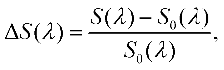 | (2) |
 | ||
| Fig. 3 Potential interaction mechanisms to explain quenching end coupling phenomena in the PLE spectra of CdSe/CdZnS QDs in MAPbBr3. (a) The relative spectral difference ΔS(λ) as defined in eqn (2), shown as a function of the excitation wavelength for samples A and B. The remaining three panels propose a band diagram of the QD-in-perovskite hybrid (energy levels of MAPbBr3 are taken as the mean values of ref. 42, 43, 44, 45, 46, 47 and 48), with associated coupling processes for (b) region I, (c) region II, and (d) region III. Electrons and holes are depicted as black and white dots, respectively; energy levels in the bad gap represent sub-band-edge defects. The excitation processes are symbolized by colored arrows (blue, green and yellow to roughly indicate the associated wavelength region) and the proposed interaction pathways are symbolized by black arrows. | ||
Fig. 3b, c and d propose a putative band alignment of the QD-in-perovskite hybrid system based on literature values.42–48 In the first scenario, region I (Fig. 3b), we indicate ancillary relaxation pathways of an electron in the conduction band of QDs that are only accessible due to presence of the perovskite matrix; while the main relaxation process in bare QDs leads to the QD conduction band edge, the hybrid sample makes it possible for the electron to be delocalized in the perovskite matrix, thus reducing the chance for radiative recombination with the hole and causing the luminescence quenching observed in region I. Such a delocalization effect is expected to become stronger with increasing excitation energy, which fits the trend shown by both films, see Fig. 3a.
Samples A and B behave differently in region II: QDs in sample A lose signal to the matrix, probably by the same quenching mechanism as in region I, while QDs in sample B gain signal from the perovskite host. Fig. 3c proposes a scenario in which coupling between the QDs and the MAPbBr3 matrix can lead to an increase of the QD signal: the putative band alignment of our QD-in-perovskite system suggests that the luminescence boost of up to 150% exhibited by sample B in region II could be the result of the creation of excitons at the perovskite band edge (λ ≈ 521 nm), followed by migration of these excitons to a nearby QD via electron relaxation and hole tunneling. This process could be conceptualized as the surrounding perovskite acting as an extended shell for the QD, thus increasing its effective absorption cross-section in region II, which can counteract the quenching effect already seen in region I to a smaller or larger degree. We speculate that the local hetero-epitaxial arrangement between the QDs and the perovskite matrix might be different for sample A and B, leading to different contributions of the two exciton migration phenomena (from QD to matrix vs. from matrix to QD). Given that the crystallization of the hybrid perovskite films depends strongly on the timing of the manual chlorobenzene injection, it is not surprising that small discrepancies from sample to sample can lead to differences in the QD–perovskite interface; further investigation will be necessary to fully understand and control this intriguing interplay of competing effects.
In region III, finally, the behavior of both films becomes similar again and is dominated by quenching (ΔS < 0). This observation may seem surprising at first, given that perovskite absorption is rather weak in this spectral region, see Fig. 1b. However, the PL spectra of samples A and B exhibit clear sub-band-edge contributions, which are usually attributed to the emission of shallow defects39,49 with small absorption cross-sections; such defects could reduce the QD emission rate by facilitating tunneling of electrons from the QD into the perovskite band edge as outlined in Fig. 3d. Confirming this hypothesis requires further studies, which could include a modification of the matrix composition by introducing chloride and/or iodide ions into the MAPbBr3 lattice to vary its band structure. We think that the charge-transfer-based mechanistic scenario proposed in this section can serve as a good starting point for further investigation and fine-tuning of the model, for example by including contributions of other interaction mechanisms such as fluorescence resonance energy transfer (FRET).
3.3 QD-in-perovskite hybrid: spatially and temporally resolved luminescence
To further investigate the coupling between the QDs and the perovskite matrix in the hybrid films, we performed spatially and temporally resolved luminescence measurements on samples A and B. Fig. 4 shows confocal photoluminescence images of a 50 × 50 μm2 of these samples, which were recorded simultaneously at the QD and MAPbBr3 wavelengths as each sample was raster-scanned through the confocal detection volume. (The QD image of sample A is rendered on a logarithmic false-color intensity scale to accommodate its dynamic range, while the other three intensity images use linear scales clipped at the 99th percentile to prevent rare high-intensity pixels from dominating the scale.) Comparing the images obtained at the QD emission wavelength, Fig. 4a/d, we find that sample A features sub-micron-sized QD clusters dispersed at a rather low surface density, while sample B shows a much more homogeneous distribution of QDs with more intense luminescence: integrating the intensities of these two QD images, we find that the overall signal of sample B is 44 times that of sample A, while the differences in doping percentage and excitation intensity between the two samples predict a B/A intensity ratio of only 4 × 3 = 12; we note that this higher-than-expected emission intensity of sample B is qualitatively consistent with the difference that we saw at 405 nm in the PLE spectra that were normalized to the same emission intensity in transparency region of perovskite, Fig. 2c. | ||
| Fig. 4 50 × 50 μm2 confocal PL intensity and lifetime images of QD-in-perovskite hybrid films, samples A (top row) and B (bottom row); pulsed excitation at 445 nm and 2 MHz repetition rate: 50 W cm−2 (sample A) and 150 W cm−2 (sample B); detection at (650 ± 15) nm (QDs) and (530 ± 5) nm (MAPbBr3); scale bar: 10 μm. Two positions of interest for the discussion of perovskite luminescence lifetimes have been marked in the images of sample A. (a) QD PL intensity on logarithmic false-color scale with contour lines at 250 counts per s. (b) MAPbBr3 PL intensity on linear false-color scale (0th to 99th percentile) with contour lines from (a) for reference. (c) Perovskite luminescence lifetime τ2, see eqn (3), on a false-color scale in which hue (blue-violet-red) indicates lifetime and color saturation is proportional to the logarithm of the intensity of each pixel; contour lines from (a) superimposed in white for reference. (d) QD PL intensity on linear false-color scale (0th to 99th percentile). (e) MAPbBr3 PL intensity on linear false-color scale (0th to 99th percentile). (f) Perovskite luminescence lifetime τ2 on the same false-color scale as (c). | ||
Focusing now on the emission intensity at the MAPbBr3 emission wavelength, Fig. 4b/e, we found similar behavior: sample B exhibited a much higher emission intensity but less structure than sample A. What is more, the perovskite signal in sample A was strongly correlated with the positions of the QD clusters, as can be seen in Fig. 4b using the contour lines from Fig. 4a as a reference. The influence of the QDs on the emission of the MAPbBr3 matrix is noticeable over a length of up to 2 μm; at the higher QD density of sample B, such an interaction can be expected to lead to a homogeneous high-intensity image at the MAPbBr3 emission wavelength, which is indeed confirmed by Fig. 4e. Our tentative interpretation of this luminescence-enhancement effect is that the QDs can act as nucleation points for the perovskite matrix; a higher degree of crystallinity should favor a higher luminescence quantum yield and thus lead to a higher luminescence signal. Overall, the perovskite image of sample B, Fig. 4e, is 6.7 times more intense than the corresponding image of sample A, while the excitation intensities differ only by a factor of three in favor of sample B.
We can in fact test our hypothesis of a QD-induced higher degree of MAPbBr3 crystallinity by looking at a second property of the emission: the luminescence lifetime of perovskite should be longer where the crystallinity of the matrix is increased, as there will be fewer defects giving rise to additional relaxation channels of the excited state. The images in Fig. 4 were acquired under pulsed-laser excitation, meaning that we measured a time-resolved lifetime curve for each pixel. (The intensity images discussed up to this point were in fact calculated from the total number of detected photons in each pixel's histogram of photon-arrival times.) To obtain MAPbBr3 lifetime images, we fitted the lifetime curves of each pixel with a biexponential function,
| I(t) = y0 + A1e−t/τ1 + A2e−t/τ2, | (3) |
The values of the slow component τ2 are represented in the MAPbBr3 lifetime images of Fig. 4c/f, which visualize τ2 on a false-color scale from blue (short lifetime, fast relaxation) to red (long lifetime, slow relaxation). The total intensity of each pixel is taken into account by color saturation, meaning that paler colors indicate lower overall count rates; a logarithmic intensity scale was used here to ensure that the hues of low-intensity pixels remain recognizable. Fig. 4c clearly shows that the perovskite lifetime in sample A is indeed longer in regions featuring a higher density of QDs, which can be identified with the help of the superimposed contour lines from the QD intensity image of the same region (Fig. 4a).
Further information on the perovskite lifetime distributions of the two samples can be found in Fig. 5. Fig. 5a illustrates the analysis of the luminescence decay curves by comparing the examples taken from the two marked pixels in Fig. 4c, which are representative for the two opposite tails of the overall τ2 distribution of sample A. This distribution itself is shown in Fig. 5b and compared to the corresponding distribution found for sample B: the lifetime distribution in sample A is highly skewed toward the long-lifetime tail, peaking around 8.5 ns and extending to more than 20 ns. The lifetime distribution in sample B, on the other hand, is an almost symmetric super-Gaussian (leptokurtic) curve centered at 12.5 ns with a FWHM of about 2 ns. In order to quantify the influence of QD presence on the luminescence lifetime of the surrounding perovskite matrix that we pointed out in the above discussion of Fig. 4c, we distinguished the pixels of this MAPbBr3 lifetime image based on their intensity in the QD luminescence image of the same region, Fig. 4a, using the threshold indicated by the contour lines. As can be seen in Fig. 5c, the distribution of perovskite lifetimes found in sample A at positions exhibiting a QD luminescence intensity of at least 250 counts per s differs significantly from the one obtained from regions of weaker QD signal: the short lifetimes making up the peak at 8.5 ns of the overall distribution (Fig. 5b) are associated with the areas of the MAPbBr3 matrix that do not contain many QDs, while a broader distribution with a median value of around 13.5 ns corresponds to the QD-rich areas. We furthermore note that this median lifetime of QD-rich pixels in sample A corresponds roughly to the maximum of the lifetime distribution found in sample B, which shows a stronger and spatially homogeneous QD signal. These results, corroborating an increased emission lifetime of the MAPbBr3 matrix at the QD locations, are consistent with our hypothesis that the QDs can act as local seeds of the MAPbBr3 host, thus contributing to a local increase in the degree of crystallinity, which in turn reduces the importance of defect-mediated exciton-relaxation pathways.
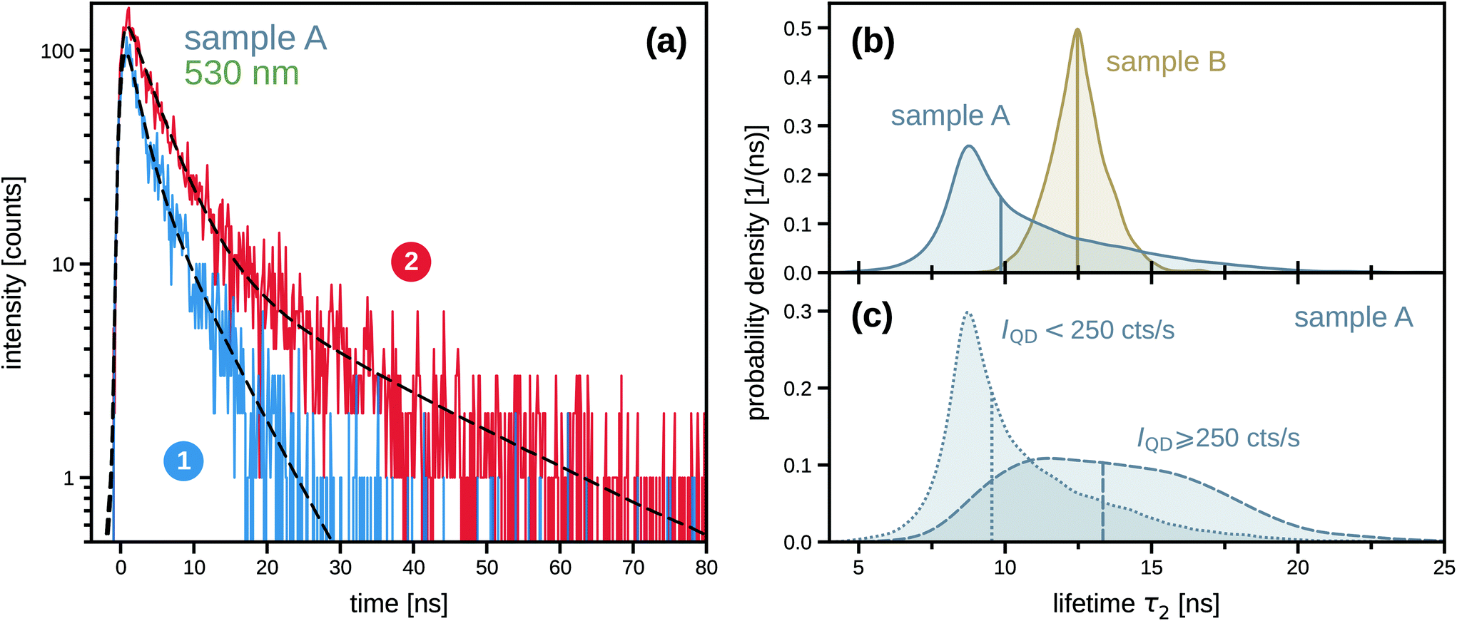 | ||
| Fig. 5 Luminescence decay curves and lifetime distributions of a QD-in-perovskite hybrid film, detected at the perovskite emission wavelength. (a) Two examples of luminescence decay curves, taken from the two pixels indicated by the numbered arrows in Fig. 4c, with biexponential fits (dashed lines), see eqn (3). Maximum-likelihood (ML) parameters for pixel 1: τ1 = (1.9 ± 0.4) ns (49% of signal), τ2 = (6.6 ± 0.9) ns (51% of signal), background 3.7% of detected photons; ML parameters for pixel 2: τ1 = (4.1 ± 0.2) ns (68% of signal), τ2 = (23.8 ± 1.5) ns (32% of signal), background 3.1%. (b) Distributions of the MAPbBr3 lifetime τ2 obtained by intensity-weighted kernel-density estimation from the τ2 values extracted from all pixels of the lifetime images of sample A (Fig. 4c) and sample B (Fig. 4f). A vertical line indicates the median of each distribution. (c) Distributions of perovskite lifetime τ2 in sample A, obtained by post-selection of pixels according to their intensity in the QD emission image (below and above 250 counts per s, see the contour lines in Fig. 4a). | ||
3.4 Individual QD-in-perovskite hybrids
We conclude our presentation of the QD-doped MAPbBr3 films by discussing samples in which we could observe single QD-in-perovskite hybrids, by which we mean embedded QDs that retain the characteristic photophysical properties of individual quantum systems, which are of particular interest for applications such as single-photon sources.50 To this end, we prepared QD-in-perovskite hybrid films with a nominal doping percentage of 0.01% (2.5× more diluted than sample A discussed above). This film was excited by a continuous-wave (CW) laser at 561 nm, i.e., in the transparency region of the MAPbBr3 host, whose luminescence signal is therefore weak, noisy and unstructured, as can be seen in Fig. 6a. The QD luminescence image of the same region of the sample, on the other hand, is structured by isolated, intense, and diffraction-limited spots, cf. Fig. 6b. We performed photon-coincidence measurements at short times of the signal originating from these single-QD spots using a Hanbury Brown and Twiss (HBT) interferometer; a typical result of which is presented in Fig. 6c. The g(2)(t) curve exhibits a clear antibunching behavior, characteristic for the emission of an individual quantum system acting as a single-photon source. We have performed this antibunching measurement on 47 individual QDs and fitted the obtained g(2)(t) functions with a single exponential rise functions,22| g(2)(t) = 1 − Ce−|t|/τQD, | (4) |
![[thin space (1/6-em)]](https://www.rsc.org/images/entities/char_2009.gif) 000 photons per s at high excitation intensities, see Fig. 6d) of the individual QD-in-perovskite hybrids. An alternative explanation is the higher refractive index of MAPbBr3, which increases the radiative relaxation rate of the embedded emitters and thus shortens the rise time without diminishing the luminescence quantum yield. As demonstrated previously, CdSe/ZnS QDs act as probes of the local refractive index with a range of sensitivity of 50–100 nm,51–53 and that furthermore their decay time in a SiO2 matrix can be predicted based on an effective medium model.35 If we use the same approach for our perovskite matrix with a refractive index of nMAPbBr3 = 2.10 (determined by ellipsometry at 650 nm) and a sensitivity radius of 80 nm of the QDs, we predict τQD ≈ 11 ns for the QD-in-perovskite hybrid (details are given in section 4 of the ESI†), in good agreement with our experimental results, which we take as further (indirect) evidence for the incorporation of the QDs in the perovskite matrix under conservation of their luminescence quantum yield.
000 photons per s at high excitation intensities, see Fig. 6d) of the individual QD-in-perovskite hybrids. An alternative explanation is the higher refractive index of MAPbBr3, which increases the radiative relaxation rate of the embedded emitters and thus shortens the rise time without diminishing the luminescence quantum yield. As demonstrated previously, CdSe/ZnS QDs act as probes of the local refractive index with a range of sensitivity of 50–100 nm,51–53 and that furthermore their decay time in a SiO2 matrix can be predicted based on an effective medium model.35 If we use the same approach for our perovskite matrix with a refractive index of nMAPbBr3 = 2.10 (determined by ellipsometry at 650 nm) and a sensitivity radius of 80 nm of the QDs, we predict τQD ≈ 11 ns for the QD-in-perovskite hybrid (details are given in section 4 of the ESI†), in good agreement with our experimental results, which we take as further (indirect) evidence for the incorporation of the QDs in the perovskite matrix under conservation of their luminescence quantum yield.
 | ||
| Fig. 6 Photoluminescence of individual QD-in-perovskite hybrids in a film with a nominal doping percentage of 0.01%. (a and b) 10 × 10 μm2 PL images under continuous-wave (CW) excitation at 561 nm with an intensity of 2.5 kW cm−2; these images were recorded simultaneously at the (a) MAPbBr3 and (b) QD emission wavelengths. Contour lines at 18 counts per ms of QD signal have been indicated in both images for reference; the scale bar represents 1 μm. (c) Photon-coincidence histogram (filled dots) measured with a two-detector Hanbury Brown – Twiss setup under CW excitation and fitted with the monoexponential model of eqn (4) (solid line, includes convolution with instrumental response), which yields τQD=(17.7 ± 0.4) ns and C = 0.77 for this particular QD. (d) Blinking timetrace of a single QD-in-perovskite hybrid under high-intensity CW excitation. | ||
Another photophysical property that has obvious implications for potential applications of single-QD emitters is their propensity to exhibit blinking, that is to say, to show intermittent luminescence under continuous excitation due to stochastic transitions into non-emissive or poorly emissive metastable states. Fig. 6d illustrates this phenomenon with a blinking timetrace of an individual QD-in-perovskite hybrid; such traces were recorded for 11 different individual QDs and compared to the blinking behavior of 12 halide-capped precursor QDs31 on glass under identical excitation conditions (λexc = 561 nm, I = 2.5 kW cm−2). Using a statistical analysis published elsewhere31 to obtain an approximate ON fraction (percentage of time spent in the highly emissive state) for each trace, we found a median value of 90% ON for the halide-capped reference QDs, while the QDs in MAPbBr3 showed a median ON fraction as large as 99% in the sample whose data is presented in Fig. 6. Two further samples with the same nominal doping percentages exhibited similar values, 94 and 96%, respectively. We thus found a consistent improvement of single-QD blinking statistics in all three samples as compared to the bare halide-capped QD precursors, while the median survival time before photobleaching under continuous excitation increased by at least 150%. (See section 5 of the ESI† for a direct comparison of blinking timetraces.) The observed small variability of the median ON time fractions is certainly influenced by many factors, crystallization being probably an important one which needs to be controlled more carefully. We think it is very encouraging that our protocol nevertheless produces such consistent results with simple manual injection of the antisolvent; further optimization of the blinking behavior and of other photophysical properties should be possible by varying the deposition conditions in a more controlled manner, which could establish QD-in-perovskite hybrids as efficient single photons sources in the visible spectral range, for which further interesting applications can be envisaged due to their coupling to the MAPbBr3 matrix that we presented in earlier sections.
4 Conclusion
To conclude, we have presented a soft-chemistry approach for doping MAPbBr3 perovskite thin films with core/gradient shell CdSe/CdZnS quantum dots (QDs) that emit in the visible spectral range. The QDs in question were synthesized with a Zn-rich shell to minimize exchange of cadmium ions with the lead ions of the perovskite matrix, and then a ligand-exchange procedure was employed to replace the native organic ligands (oleic acid) of the QDs with halide ions (chloride and bromide) to improve compatibility with the MAPbBr3 host and ensure QD dispersibility with the perovskite precursors in DMF. Our protocol yielded QD-in-perovskite hybrid films with thicknesses of around 100 nm and nominal doping percentages (volume/volume) that could be adjusted between 0.01 and 1%. The samples all showed stable photoluminescence (PL) emission of both the perovskite host (around 530 nm) and the QD guest (around 650 nm), whose relative intensity scaled roughly linearly with the doping level. We then focused our study on two samples with a doping percentage of 0.025 and 0.1%, respectively, whose PL spectra were comparable after correction for doping level, but whose photoluminescence-excitation (PLE) spectra differed substantially even after a normalization procedure based on equalizing their average intensities in the transparency window of the MAPbBr3 matrix. To explain these intriguing observations, we propose a model based on three distinct perovskite-QD coupling processes, whose wavelength-dependent interplay can vary from sample to sample: first, at high excitation energies, additional relaxation channels of the QD excitons exist due to escape of electrons into the conduction band of the MAPbBr3 matrix; second, at excitation energies close to that of the perovskite exciton, electrons and holes created in the matrix can tunnel to a nearby QD, thus boosting its luminescence by a factor of up to 2.5; and, finally, in a narrow energy region that matches shallow defects of the MAPbBr3 matrix, electrons can be transferred from the QDs to those defects.Local PL measurements by confocal microscopy show that the MAPbBr3 matrix emission signal increases at the QD locations in our doped thin films, suggesting that a higher degree of crystallinity is facilitated by the inclusion of the QDs, which seem to act as seeds in the perovskite crystallization process; the radius of influence of this effect was estimated to be about 2 μm. This nucleation-seed hypothesis was further corroborated by lifetime imaging, which revealed that the emission lifetime of the MAPbBr3 matrix does indeed increase in the vicinity of QD clusters, as is expected in regions where higher crystal quality reduces the number of defect-mediated relaxation channels of the perovskite exciton.
We furthermore demonstrated that individual QDs in MAPbBr3 act as single-photon emitters at sustained count rates of up to 800000 photons per s, which shows that this hybrid system has potential as stable single-photon source in the visible, especially since we noted that the blinking characteristics of the single emitters were actually improved (less time spent in dark or dim states) by incorporation in the perovskite host. Given these favorable photophysical properties and the fact that the doping percentage can be varied over at least two orders of magnitude, our present results offer many intriguing perspectives for applications of the QD-in-perovskite hybrid, for example hybrid-based solar-cell concentrators with QDs emitting in the visible range at high doping percentages, or photonic devices for single-photon optical circuits at low doping levels.
Author contributions
Conceptualization, J. H. and B. M.; data curation, J. B.; formal analysis, J. B., J. H. and F. K.; funding acquisition, J. H. and C. D.; investigation, J. B.; methodology, J. H., F. K. and B. M.; project administration, J. H.; resources, J. H. (optical experiments) and B. M. (chemistry); software, F. K. (data acquisition, maximum-likelihood analysis); supervision, J. H., F. K. and B. M.; validation, J. B. and B. M. (chemistry protocols), J. B. and J. H. (optical experiments); visualization, J. H. and F. K.; writing – original draft, J. H.; writing – review & editing, J. H. and F. K.Conflicts of interest
There are no conflicts to declare.Acknowledgements
The authors thank J.-F. Sivignon, Y. Guillin, G. Montagne and the Lyon center for nano-opto technologies (NanOpTec) for technical support. This work was financially supported by the Agence Nationale de Recherche (ANR-16-CE24-0002), IDEXLYON of Université de Lyon in the framework “Investissement d'Avenir” (ANR-IDEX-0005) and the Fédération de Recherche André–Marie Ampère (FRAMA).References
- A. Kojima, K. Teshima, Y. Shirai and T. Miyasaka, J. Am. Chem. Soc., 2009, 131, 6050 CrossRef CAS PubMed.
- H. Min, D. Lee, J. Kim, G. Kim, K. S. Lee, J. Kim, M. J. Paik, Y. K. Kim, K. S. Kim, M. G. Kim, T. J. Shin and S. I. Seok, Nature, 2021, 598, 444–463 CrossRef CAS PubMed.
- H. T. Wei and J. S. Huang, Nat. Commun., 2019, 10, 1066 CrossRef PubMed.
- Q. A. Akkerman, G. Rainò, M. V. Kovalenko and L. Manna, Nat. Mater., 2018, 17, 394–405 CrossRef CAS PubMed.
- Y. P. Fu, H. M. Zhu, J. Chen, M. P. Hautzinger, X. Y. Zhu and S. Jin, Nat. Rev. Mater., 2019, 4, 169–188 CrossRef CAS.
- V. B. Mykhaylyk, H. Kraus and M. Saliba, Mater. Horiz., 2019, 6, 1740–1747 RSC.
- W. L. Yu, F. Li, L. Y. Yu, M. R. Niazi, Y. T. Zou, D. Corzo, A. Basu, C. Ma, S. Dey, M. L. Tietze, U. Buttner, X. B. Wang, Z. H. Wang, M. N. Hedhili, C. L. Guo, T. Wu and A. Amassian, Nat. Commun., 2018, 9, 5354 CrossRef CAS PubMed.
- S. D. Stranks and H. J. Snaith, Nat. Nanotechnol., 2015, 10, 391–402 CrossRef CAS PubMed.
- H. Utzat, W. W. Sun, A. E. K. Kaplan, F. Krieg, M. Ginterseder, B. Spokoyny, N. D. Klein, K. E. Shulenberger, C. F. Perkinson, M. V. Kovalenko and M. G. Bawendi, Science, 2019, 363, 1068 CrossRef CAS PubMed.
- N. G. Park, M. Grätzel, T. Miyasaka, K. Zhu and K. Emery, Nat. Energy, 2016, 1, 16152 CrossRef CAS.
- Z. J. Ning, X. W. Gong, R. Comin, G. Walters, F. J. Fan, O. Voznyy, E. Yassitepe, A. Buin, S. Hoogland and E. H. Sargent, Nature, 2015, 523, 324–328 CrossRef CAS PubMed.
- J. Ge, W. X. Li, X. He, H. Chen, W. Fang, X. Du, Y. X. Li and L. Zhao, Sustainable Energy Fuels, 2020, 4, 1837–1843 RSC.
- C. Fan, X. Xu, K. Yang, F. Jiang, S. Y. Wang and Q. L. Zhang, Adv. Mater., 2018, 30, 1804707 CrossRef PubMed.
- X. S. Tang, J. Yang, S. Q. Li, Z. Z. Liu, Z. P. Hu, J. Y. Hao, J. Du, Y. X. Leng, H. Y. Qin, X. Lin, Y. Lin, Y. X. Tian, M. Zhou and Q. H. Xiong, Adv. Sci., 2019, 6, 1900412 CrossRef CAS PubMed.
- V. K. Ravi, S. Saikia, S. Yadav, V. V. Nawale and A. Nag, ACS Energy Lett., 2020, 5, 1794–1796 CrossRef CAS.
- M. G. Bawendi, in Confined Electrons and Photons: New Physics and Applications, ed. E. Burstein and C. Weisbuch, Springer US, Boston, MA, 1995, vol. 340 of NATO Advanced Science Institutes Series, Series B, Physics, pp. 339–356 Search PubMed.
- B. Mahler, P. Spinicelli, S. Buil, X. Quélin, J. P. Hermier and B. Dubertret, Nat. Mater., 2008, 7, 659–664 CrossRef CAS PubMed.
- D. Bozyigit, O. Yarema and V. Wood, Adv. Funct. Mater., 2013, 23, 3024–3029 CrossRef CAS.
- H. Zhang, K. Cheng, Y. M. Hou, Z. Fang, Z. X. Pan, W. J. Wu, J. L. Hua and X. H. Zhong, Chem. Commun., 2012, 48, 11235–11237 RSC.
- F. Huang, L. S. Zhang, Q. F. Zhang, J. Hou, H. G. Wang, H. L. Wang, S. L. Peng, J. S. Liu and G. Z. Cao, ACS Appl. Mater. Interfaces, 2016, 8, 34482–34489 CrossRef CAS PubMed.
- M. G. Hyldahl, S. T. Bailey and B. P. Wittmershaus, Sol. Energy, 2009, 83, 566–573 CrossRef CAS.
- B. Lounis, H. A. Bechtel, D. Gerion, P. Alivisatos and W. E. Moerner, Chem. Phys. Lett., 2000, 329, 399–404 CrossRef CAS.
- L. Biadala, Y. Louyer, P. Tamarat and B. Lounis, Phys. Rev. Lett., 2009, 103, 037404 CrossRef CAS PubMed.
- M. J. Fernée, C. Sinito, Y. Louyer, C. Potzner, T. L. Nguyen, P. Mulvaney, P. Tamarat and B. Lounis, Nat. Commun., 2012, 3, 1287 CrossRef PubMed.
- M. J. Fernée, C. Sinito, Y. Louyer, P. Tamarat and B. Lounis, Nanotechnology, 2013, 24, 465703 CrossRef PubMed.
- U. Woggon, E. Herz, O. Schöps, M. V. Artemyev, C. Arens, N. Rousseau, D. Schikora, K. Lischka, D. Litvinov and D. Gerthsen, Nano Lett., 2005, 5, 483–490 CrossRef CAS PubMed.
- M. Rashad, M. Paluga, A. Pawlis, K. Lischka, D. Schikora, M. V. Artemyev and U. Woggon, Phys. Status Solidi C, 2010, 7, 1523–1525 CrossRef CAS.
- R. J. Warburton, C. Schaflein, D. Haft, F. Bickel, A. Lorke, K. Karrai, J. M. Garcia, W. Schoenfeld and P. M. Petroff, Nature, 2000, 405, 926–929 CrossRef CAS PubMed.
- Z. B. Li, H. A. Li, K. Jiang, D. Ding, J. N. Li, C. Ma, S. C. Jiang, Y. Wang, T. D. Anthopoulos and Y. M. Shi, ACS Appl. Mater. Interfaces, 2019, 11, 40204–40213 CrossRef CAS PubMed.
- J. Lim, B. G. Jeong, M. Park, J. K. Kim, J. M. Pietryga, Y. S. Park, V. I. Klimov, C. Lee, D. C. Lee and W. K. Bae, Adv. Mater., 2014, 26, 8034–8040 CrossRef CAS PubMed.
- J. Baronnier, B. Mahler, O. Boisron, C. Dujardin, F. Kulzer and J. Houel, Phys. Chem. Chem. Phys., 2021, 23, 22750–22759 RSC.
- R. Comin, G. Walters, E. S. Thibau, O. Voznyy, Z. H. Lu and E. H. Sargent, J. Mater. Chem. C, 2015, 3, 8839–8843 RSC.
- Y. Yu, S. W. Yang, L. Lei, Q. P. Cao, J. Shao, S. Zhang and Y. Liu, ACS Appl. Mater. Interfaces, 2017, 9, 3667–3676 CrossRef CAS PubMed.
- L. L. Yang, Y. B. Gao, Y. J. Wu, X. X. Xue, F. Y. Wang, Y. R. Sui, Y. F. Sun, M. B. Wei, X. Y. Liu and H. L. Liu, ACS Appl. Mater. Interfaces, 2019, 11, 792–801 CrossRef CAS PubMed.
- A. Aubret, V. Dolique, A. Piednoir, C. Dujardin, F. Kulzer and J. Houel, Semicond. Sci. Technol., 2020, 35, 055005 CrossRef CAS.
- T. Zhao, H. B. Liu, M. E. Ziffer, A. Rajagopal, L. J. Zuo, D. S. Ginger, X. S. Li and A. K. Y. Jen, ACS Energy Lett., 2018, 3, 1662–1669 CrossRef CAS.
- D. Y. Guo, D. Bartesaghi, H. T. Wei, E. M. Hutter, J. S. Huang and T. J. Savenije, J. Phys. Chem. Lett., 2017, 8, 4258–4263 CrossRef CAS PubMed.
- Y. T. Liu, H. Z. Lu, J. X. Niu, H. T. Zhang, S. T. Lou, C. L. Gao, Y. Q. Zhan, X. L. Zhang, Q. Y. Jin and L. R. Zheng, AIP Adv., 2018, 8, 095108 CrossRef.
- P. Kumar, Q. Shi and K. J. Karki, J. Phys. Chem. C, 2019, 123, 13444–13450 CrossRef CAS.
- S. G. Motti, D. Meggiolaro, S. Martani, R. Sorrentino, A. J. Barker, F. De Angelis and A. Petrozza, Adv. Mater., 2019, 31, 1901183 CrossRef CAS PubMed.
- N. J. Jeon, J. H. Noh, Y. C. Kim, W. S. Yang, S. Ryu and S. I. Seok, Nat. Mater., 2014, 13, 897–903 CrossRef CAS PubMed.
- S. Adjokatse, H. H. Fang and M. A. Loi, Mater. Today, 2017, 20, 413–424 CrossRef CAS.
- J. H. Noh, S. H. Im, J. H. Heo, T. N. Mandal and S. I. Seok, Nano Lett., 2013, 13, 1764–1769 CrossRef CAS PubMed.
- S. Ryu, J. H. Noh, N. J. Jeon, Y. C. Kim, S. Yang, J. W. Seo and S. I. Seok, Energy Environ. Sci., 2014, 7, 2614–2618 RSC.
- L. C. Chen, J. R. Wu, Z. L. Tseng, C. C. Chen, S. H. Chang, J. K. Huang, K. L. Lee and H. M. Cheng, Materials, 2016, 9, 747 CrossRef PubMed.
- T. Zhang, J. Wu, P. Zhang, W. Ahmad, Y. F. Wang, M. Alqahtani, H. Chen, C. M. Gao, Z. D. Chen, Z. M. Wang and S. B. Li, Adv. Opt. Mater., 2018, 6, 1701341 CrossRef.
- P. Schulz, E. Edri, S. Kirmayer, G. Hodes, D. Cahen and A. Kahn, Energy Environ. Sci., 2014, 7, 1377–1381 RSC.
- H. Kim, K. G. Lim and T. W. Lee, Energy Environ. Sci., 2016, 9, 12–30 RSC.
- G. Delport, G. Chehade, F. Lédée, H. Diab, C. Milesi-Brault, G. Trippé-Allard, J. Even, J. S. Lauret, E. Deleporte and D. Garrot, J. Phys. Chem. Lett., 2019, 10, 5153–5159 CrossRef CAS PubMed.
- B. Lounis and M. Orrit, Rep. Prog. Phys., 2005, 68, 1129–1179 CrossRef CAS.
- V. LeBihan, A. Pillonnet, D. Amans, G. Ledoux, O. Marty and C. Dujardin, Phys. Rev. B: Condens. Matter Mater. Phys., 2008, 78, 113405 CrossRef.
- A. Aubret, A. Pillonnet, J. Houel, C. Dujardin and F. Kulzer, Nanoscale, 2016, 8, 2317–2325 RSC.
- A. Aubret, J. Houel, A. Pereira, J. Baronnier, E. Lhuillier, B. Dubertret, C. Dujardin, F. Kulzer and A. Pillonnet, ACS Appl. Mater. Interfaces, 2016, 8, 22361–22368 CrossRef CAS PubMed.
Footnote |
| † Electronic supplementary information (ESI) available: Gaussian fits of PL spectra, normalization of PLE spectra, influence of the refractive index on the radiative lifetime. See DOI: https://doi.org/10.1039/d1nr08473a |
| This journal is © The Royal Society of Chemistry 2022 |