
 Open Access Article
 This Open Access Article is licensed under a
 Creative Commons Attribution 3.0 Unported Licence
Wafer-sized WS2 monolayer deposition by sputtering
Michelle Marie S.
Villamayor
a,
Sajid
Husain
bc,
Reinier
Oropesa-Nuñez
 b,
Fredrik O. L.
Johansson
d,
Rebecka
Lindblad
e,
Pedro
Lourenço
f,
Romain
Bernard
f,
Nadine
Witkowski
f,
Geoffroy
Prévot
f,
Nomi L. A. N.
Sorgenfrei
gh,
Erika
Giangrisostomi
g,
Alexander
Föhlisch
gh,
Peter
Svedlindh
b,
Andreas
Lindblad
*d and
Tomas
Nyberg
a
b,
Fredrik O. L.
Johansson
d,
Rebecka
Lindblad
e,
Pedro
Lourenço
f,
Romain
Bernard
f,
Nadine
Witkowski
f,
Geoffroy
Prévot
f,
Nomi L. A. N.
Sorgenfrei
gh,
Erika
Giangrisostomi
g,
Alexander
Föhlisch
gh,
Peter
Svedlindh
b,
Andreas
Lindblad
*d and
Tomas
Nyberg
a
aDivision of Solid State Electronics, Department of Electrical Engineering, Uppsala University, Box 65, SE-751 03 Uppsala, Sweden
bDivision of Solid State Physics, Department of Materials Science and Engineering, Uppsala University, Box 35, SE-751 03 Uppsala, Sweden
cUnité Mixte de Physique, CNRS, Thales, Université Paris-Saclay, 91767 Palaiseau, France
dDivision of X-ray Photon Science, Department of Physics & Astronomy, Uppsala University, Box 516, SE-751 20 Uppsala, Sweden. E-mail: andreas.lindblad@physics.uu.se
eDivision of Inorganic Chemistry, Department of Chemistry-Ångström, Uppsala University, Box 521, SE-751 20 Uppsala, Sweden
fSorbonne Université, CNRS, Institut des NanoSciences de Paris, INSP, F-75005, Paris, France
gInstitute for Methods and Instrumentation for Synchrotron Radiation Research, Helmholtz-Zentrum Berlin für Materialien und Energie GmbH, Albert-Einstein-Straße 15, 12489 Berlin, Germany
hInstitut für Physik und Astronomie, Universität Potsdam, Karl-Liebknecht-Straße 24/25, 14476 Potsdam, Germany
First published on 14th March 2022
Abstract
We demonstrate that tungsten disulphide (WS2) with thicknesses ranging from monolayer (ML) to several monolayers can be grown on SiO2/Si, Si, and Al2O3 by pulsed direct current-sputtering. The presence of high quality monolayer and multilayered WS2 on the substrates is confirmed by Raman spectroscopy since the peak separations between the A1g-E2g and A1g-2LA vibration modes exhibit a gradual increase depending on the number of layers. X-ray diffraction confirms a textured (001) growth of WS2 films. The surface roughness measured with atomic force microscopy is between 1.5 and 3 Å for the ML films. The chemical composition WSx (x = 2.03 ± 0.05) was determined from X-ray Photoelectron Spectroscopy. Transmission electron microscopy was performed on a multilayer film to show the 2D layered structure. A unique method for growing 2D layers directly by sputtering opens up the way for designing 2D materials and batch production of high-uniformity and high-quality (stochiometric, large grain sizes, flatness) WS2 films, which will advance their practical applications in various fields.
1. Introduction
Monolayer two dimensional (2D) transition metal dichalcogenides (TMDCs) recently gained attention due to their excellent electrical, optical and magnetic properties.1,2 Because of their semiconducting characteristics, TMDCs provide the possibility to overcome the shortcomings of zero-bandgap materials, like graphene. Tungsten disulfide (WS2) is one of the most studied 2D-TMDCs, and is a layered material similar to graphene. A layer of a TMDC is typically 6–8 Å thick and consists of one plane of metal atoms sandwiched between two planes of chalcogen atoms – in the planes, the atoms are arranged in hexagonal patterns. Consecutive layers are held together by weak van der Waals forces. Whereas bulk WS2 has an indirect band gap of 1.3 eV, a monolayer has a direct band gap reported to be slightly lower than 2.05 eV since the direct electronic transitions in WS2 originate from excitonic radiative relaxation.3,4 FET devices based on monolayer WS2 exhibit an excellent ON/OFF current ratio of 108 and carrier mobility greater than 200 cm2 V−1 (s−1).5 The strong photoluminescence of WS2 makes it a possible component for future electronic and optoelectronic devices. Its potential applications include transistors, lithium-ion batteries, solid lubricants, chemical sensors, membranes, heterogeneous catalysis especially for the hydrogen evolution reaction (HER) in photocatalytic water splitting, and spintronics.6,7Several methods can be used to grow WS2 films on various substrates. Chemical vapor deposition (CVD) is the most common process to grow TMDCs.8–15 However related methods, including atomic layer deposition (ALD)6,16 and metal–organic CVD (MOCVD)7,17,18 have been used. Also exfoliation of monolayer, or few layers of a dichalcogenide have been achieved.10,19
The biggest issue of these methods is that they are unsuitable for the growth of large area films. They produce small areas, or even flake sizes in the case of exfoliation methods.20 Xu et al., have reported large-scale deposition of monolayer WS2 on SiO2/Si substrate that resulted in triangular flakes with 12.7 μm sides.12 Another approach is to sputter from a W target and then post-anneal the metal film in sulfur atmosphere.14
A two-stage process has been developed to prepare high quality bilayer TMDC stacking using reverse-flow chemical vapor epitaxy.21 Recently, Zhang and co-workers22 succeeded in 6-inch wafer size growth of TMDCs e.g. MoS2. Monolayers of MoS2 were grown using a low pressure face-to-face precursor CVD method where the Mo sheet is kept in front of a soda-lime glass substrate. This process allows large-scale wafer size TMDC production. However, during transfer of the TMDCs onto a different substrate, large strain and cracks develop – a shortcoming of this indirect growth method. High quality TMDCs were also successfully deposited on SiO2 substrates using a two-step process where a metal film is deposited on a substrate followed by sulfurization.23,24
Monolayer TMDC films can be produced by CVD, MOCVD and ALD as outlined above. For instance, wafer-sized specimens synthesised by these techniques are available commercially.
Several attempts have been made to grow TMDCs using sputtering, including MoS2![[thin space (1/6-em)]](https://www.rsc.org/images/entities/char_2009.gif) 25 and WS226 on various substrates such as sapphire Al2O3, glass, and Si/SiO2, but issues relating to film quality when grown on Si/SiO2 substrates have been reported. To grow WS2 films, Regula et al. have used a sintered WS2 target in Ar/H2S atmosphere (H2S 0–10%), where the substrate was electrically grounded, and heated at 600 °C at a process pressure between 7.5–9 mTorr.27 The group of Ellmer explored the effect of different process parameters (substrate temperature, amount of reactive gas, sputtering pressure, substrate material, process gas) using a W target for sputter depositing WS2.28,29 Process parameters for growth of multilayer WS2 films by sputtering from a WS2 have been reported earlier by our group.30
25 and WS226 on various substrates such as sapphire Al2O3, glass, and Si/SiO2, but issues relating to film quality when grown on Si/SiO2 substrates have been reported. To grow WS2 films, Regula et al. have used a sintered WS2 target in Ar/H2S atmosphere (H2S 0–10%), where the substrate was electrically grounded, and heated at 600 °C at a process pressure between 7.5–9 mTorr.27 The group of Ellmer explored the effect of different process parameters (substrate temperature, amount of reactive gas, sputtering pressure, substrate material, process gas) using a W target for sputter depositing WS2.28,29 Process parameters for growth of multilayer WS2 films by sputtering from a WS2 have been reported earlier by our group.30
The sputtering technique is a versatile and promising method for cost-efficient large scale industrial production of TMDCs – a scope unavailable to, e.g. the resource intensive CVD-technique.
Synthesizing TMDC monolayers over large areas (wafer-scale) using sputtering techniques would thus be a route providing industrially viable application of these materials. Tao et al., deposited MoS2 monolayers by sputtering of Mo together with evaporated sulphur.25 To our knowledge, no one has produced a large scale monolayer TMDC by sputtering from a TMDC target without co-evaporation or post-processing (e.g. sulphurization or annealing).
In this paper we report on high quality WS2 large area monolayers directly grown on 500 nm SiO2 on Si, Si, and sapphire substrates. We have used a WS2 target together with H2S atmosphere as described below. The quality of the films has been verified by several methods: Raman spectroscopy, atomic force microscopy (AFM), photoluminescence (PL), cross sectional transmission electron microscopy (TEM), X-ray diffraction (XRD) and X-ray photoelectron spectroscopy (XPS).
2. Methods
2.1. Film preparation
WS2 films were deposited using a CS 600 von Ardenne high vacuum magnetron sputtering system. The magnetron was located on the top lid of the deposition chamber with a 45° angle towards the substrate table at the center of the chamber bottom shown as shown in Fig. 1(a). The target-substrate distance was fixed to 16 cm. Substrates (SiO2/Si, Si and Al2O3) were located in front of the target and heated to 700 °C during deposition. | ||
| Fig. 1 (a) Schematic diagram of the sputter source used to deposit a monolayer and few layers of WS2. (b) A 4-inch diameter wafer with 1 monolayer WS2 on SiO2 substrate. | ||
The base pressure was 10−7 Torr for all depositions. A 100 mm WS2 target (99.9% purity, K. Lesker, Inc.) was powered with a 200 W pulsed-DC at 20 kHz frequency. The working pressure was kept constant at 50 mTorr with H2S flow rate of 20 sccm. The deposition time for one monolayer WS2 was around 2 minutes resulting in a film covering a whole 4 inch wafer as shown in Fig. 1(b).
2.2. Characterization
3. Results and discussion
3.1. Raman spectroscopy
In WS2 the first order phonon modes that occur at the Brillouin zone centre (Γ) are: A1g, 2A2u, 2B2g, B1u, E1g, 2E1u, 2E2g, and, E2u. A2u and E1u are acoustic modes and infrared active. A1g, E1g, and E2g, are Raman active. B2g, B1u, and E2u are undetected optically. In addition to these, a longitudinal acoustic (LA) mode at the (M) symmetry point of the Brillouin zone exists in these TMDCs due to the collective in-plane movement of the atoms in the lattice.38 Note that the 2LA is the second harmonic mode39 appear due to the laser excitation and it can reduce with laser wavelength.38 Moreover, the 2LA intensity is suppressed in more than one layer of WS2, which confirmed the higher layer numbers of WS2 (discussed later). The LA mode overlaps at the Γ point with the E2g mode.Fig. 2 shows the Raman spectra recorded on monolayer and few layers WS2. The peak positions are extracted by multi-peak least squares fit of Lorentzian peaks to the data. These Raman spectra mainly show A1g at 418.27 ± 0.06 cm−1, E2g at 358.50 ± 0.11 cm−1, and 2LA at 354.42 ± 0.42 cm−1. The uncertainty in the peak position is the standard error obtained from the least squares multi-peak fit. These peak positions are representative of monolayer of WS2 at 300 K.40 Notice that low intensity peaks observed at low wavenumber around 300 and 325 cm−1 correspond to the out-of-plane acoustic phonon modes ascribed to the edge of the M-point in the Brillouin zone.41
 | ||
| Fig. 2 Raman spectra as a function of number of layers recorded on: (a) a monolayer (1ML), (b) bilayer (2ML), (c) four layer (4ML), and (d) eight layer (8ML), sample. (e) Peak separation A1g-2LA, and (f) A1g–E2g. The theory data points are from ref. 31, experimental data: blue circles,32 red circles,33 red squares,34 red triangles,35 The grey rectangle in (f) indicate the observed peak separations in the Raman mapping discussed in the text and shown in Fig. 4. | ||
When we increase the number of WS2 layers, the peak positions are shifted with growing peak separation. For bilayer WS2, peak positions for A1g, E2g, and 2LA are observed at 418.27 ± 0.06 cm−1, 356.37 ± 0.13 cm−1, and 350.9 ± 0.37 cm−1, respectively. Further increasing the number of WS2 layers increases the peak separation as shown in Fig. 2(e) and (f) for A1g-2LA and A1g-E2g, respectively. This peak separation indicates the formation of one, two, and so on layers towards bulk WS2. Comparably, our results agree with those of Shi et al.,40 and theoretical predictions31 rather than earlier experimental reports of peak separations of WS2 on monolayer to bulk samples.34,35,38,42 The peak intensity ratio is calculated as shown in Fig. 3. Relative intensity ratios of the 2LA and A1g phonon modes for mono- and bi-layer samples agrees with reported results.38 An intensity ratio close to 2 indicates the presence of a monolayer.41
 | ||
| Fig. 3 Peak intensity ratio of E2g, A1g, and 2LA as function of number of layers. | ||
In order to determine the film uniformity, Raman mapping was performed on a 60 × 60 mm2 area of a 4-inch SiO2/Si wafer. Fig. 4 shows the map of the separation between the two peak positions of A1g–E2g. The mapindicate that the thickness is uniform over the whole 4-inch wafer. Raman mapping shows a narrow spread of the spacing around the value expected for a monolayer (59.9 cm−1). The peak separation is within the spread indicated with a grey rectangle in Fig. 2(f). The mapping thus exhibits a high quality monolayer growth on a large area substrate. This demonstrates the industrial compatibility of WS2 directly grown on SiO2 substrates.
 | ||
| Fig. 4 (a) Raman mapping showing peak separation of A1g–E2g on very large area monolayer WS2 sample on SiO2/Si. The peak separations were measured every 10 mm over area of 60 × 60 mm2 here presented with the points linearly interpolated. The black dots indicate where the peak separations have been measured. The white area is centered on a position where no data was acquired. The range is represented by the gray rectangle in Fig. 2(f). | ||
3.2. Photoluminescence (PL) spectroscopy
Fig. 5 shows the photoluminescence spectra of monolayer and bilayer WS2 grown on SiO2 substrate. The main peak is centered at 2.03 eV for the monolayer sample. The small peaks at 2.17 eV to 2.20 eV are Raman modes. There was significantly smaller photoluminescence signal observed for the bilayer sample. These observations agree with previous computations and experimental results.3,4,35,43–48 | ||
| Fig. 5 The PL spectrum of the WS2 monolayer (black) has its peak intensity at 2.03 eV. No significant PL peak was observed for the bilayer sample (red). | ||
3.3. X-Ray photoelectron spectroscopy (XPS)
The core level photoelectron spectra recorded on WS2 monolayer grown on SiO2 substrates are shown in Fig. 6. A survey spectrum is shown in the bottom panel where we identify signatures at binding energies from: overlayer W, S (corresponding to WS2 binding energies49); substrate Si and O (at SiO2 binding energy positions50) and C species adsorbed on the surface51 – we also find trace amounts of Ag.52 The horizontal lines indicate the distance from the main peak to the plasmon excitation.53,54 The C 1s core level (at binding energy 284 eV) do not have a plasmon which indicate that this element is weakly adsorbed on the surface. | ||
| Fig. 6 X-ray photoelectron spectra of sputter-deposited WS2 monolayer (orange circles). The W 4f-core level spectrum is to the left and the S 2p-core level spectrum to the right. The components from a least squares fit to the data are also included. The positions of the spin orbit components are indicated with vertical lines. A survey spectrum is presented at the bottom with assignment of the core levels. Horisontal lines indicate the distance in energy from a main line to the plasmon peaks discussed in the text. | ||
The recorded spectra have been fitted with spin–orbit components for the W 4f and S 2p-core levels. The peaks corresponding to the W 5p3/2, W 4f5/2, and W 4f7/2 orbitals are observed at 37.9, 34.6 and 32.5 eV, respectively. The peak position of W 4f7/2 (32.5 eV) is at larger binding energy compared to metallic W 4f7/2 (31.6 eV). For sulfur, the 2p1/2 and 2p3/2 binding energies are at 163.3 eV 162.1 eV respectively. The binding energies indicate the valence state of the material, and are consistent with a 4+ valence state of tungsten, corresponding to a S:W ratio of 2, i.e. stoichiometric WS2.15 The chemical composition WSx (x = 2.03 ± 0.05) was obtained from a least squares fit to the data (Fig. 6). Compared with thicker films obtained using the same deposition parameters for which the S/W ratio was found equal to 1.86,30 monolayer films are thus found to be stochiometric.
3.4. Atomic force microscopy (AFM)
Fig. 7 displays the topography of the WS2 films on the SiO2/Si, Si, Al2O3 substrates using AFM. The measured surface roughness σa is also indicated on each sample. On the SiO2/Si substrate, monolayer films present an atomically smooth surface (surface roughness, 3 Å). The roughness increases slightly with increasing number of layers (1 to 8 layers) – for a 8 layer film, we measured a surface roughness of 7 Å. Monolayers with small roughness are also found in the case of Si and Al2O3 substrates. However, increasing the number of WS2 layers leads to a significant increase in the surface roughness on Si and Al2O3 substrates. On those substrates, layers grow rougher than those grown on SiO2/Si (top row in Fig. 7). Note that on the Al2O3 substrate the bi-layer have a small surface roughness compared to the other bilayers. For bulk thicknesses, grain-like features that add to the to the larger surface roughness are observed.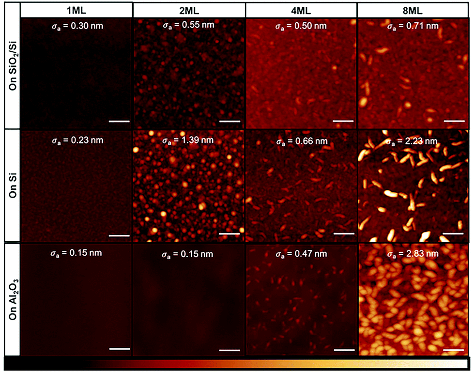 | ||
| Fig. 7 Topographical analysis from AFM of WS2 deposited on SiO2/Si, Si, and Al2O3 substrates and the measured surface roughness σa. (Scale bar: 200 nm; Z scale: 25 nm.) | ||
From this analysis, we can understand that the growth is highly substrate dependent. It is visible that W and S atoms easily bond together when deposited on SiO2 substrate which follow layer by layer growth even in the bulk regime, Fig. 7 (top panel 8ML). Layer by layer growth also occur on Al2O3 substrate up to three layers, but island formation starts after four layers as shown in Fig. 7 (bottom panel 8ML). In case of Si, the growth is mixed, where the small flakes are formed in high number layers with layer-like growth. Thus it is clear that the TMDC growth is substrate dependent which was also observed previously,55 and also depends on deposition conditions.30
3.5. Transmission electron microscopy (TEM)
To further verify the layer-by-layer growth and thickness of WS2 layers, high resolution cross-sectional TEM imaging was performed on a thick film shown in Fig. 8. The total thickness of this film is 26 nm. The thickness of each layer of WS2 was found to 7 Å. A zoomed cross section is shown in the inset with atomic positions marked with colored spheres, green for W and yellow for S.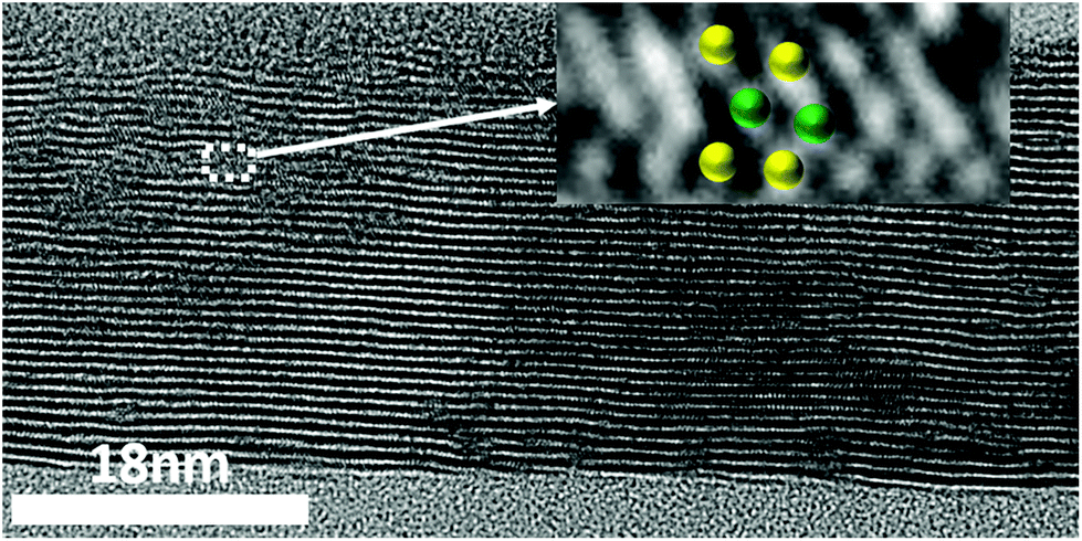 | ||
| Fig. 8 High resolution cross-sectional TEM image of several layers of WS2. Inset is zoomed area of one monolayer WS2 marked by spheres of different colors: green (W) and yellow (S). | ||
3.6. X-Ray diffraction
Fig. 9(a) shows the XRD spectra for 8 monolayer WS2 film deposited on SiO2/Si, Si and Al2O3 substrates. All the films exhibit a strong orientation along the (001) direction which indicate the crystalline nature of WS2 growth on all different substrates. The intensity of the [002] peak is highest for the Al2O3, followed by that on the Si, and then the SiO2/Si substrate. The peak positions are identically matched with the commercially available high quality single crystal.56Fig. 9(b) shows the in-plane XRD pattern for 2, 4 and 8 monolayers of WS2 film deposited on SiO2/Si. The in-plane lattice constant evolves from 0.3151 nm for the 2 ML thick film to 0.3140 nm for the 8 ML thick film.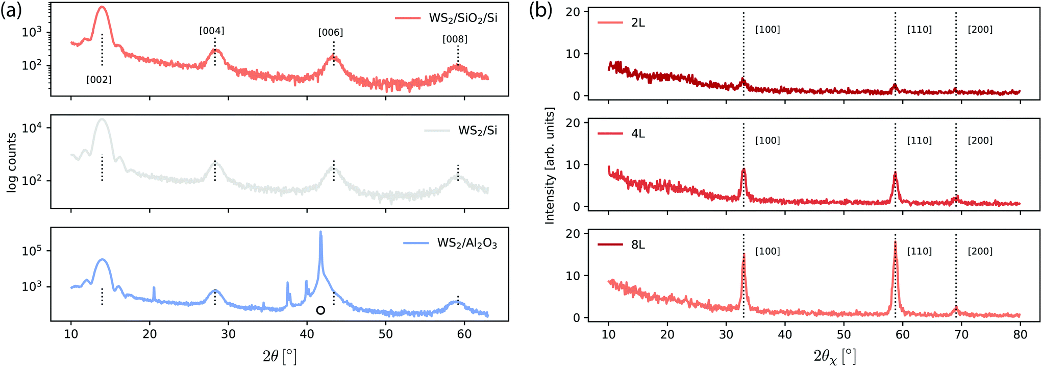 | ||
| Fig. 9 (a) X-ray diffraction patterns of 8 monolayers of WS2 deposited on different substrates. The main substrate peak is indicated by a solid circle (peaks at 20, 35, 38 and 40 degrees are also from the substrate). (b) In-plane X-ray diffraction patterns of 2, 4 and 8 monolayers of WS2/SiO2/Si. | ||
The in plane measurements indicate the presence of polycristalline flakes with domain sizes of the order of 10–20 nm – estimated from using the Scherrer equation and the FWHM of the [100] peak with shape factor 0.9.57
4. Conclusions
We have successfully grown stoichiometric monolayer (and multilayer) films of WS2 on wafer-size substrates of SiO2/Si, Si and Al2O3. The stoichiometry of the film was verified by XPS and the uniformity by Raman mapping. The (001) texture of the WS2 films is confirmed using X-ray diffraction analysis for all substrates. Raman spectroscopy and Photoluminescence measurements discriminate between the deposition of monolayer and few layers WS2. Atomic Force Microscopy shows the uniform growth and the atomic smoothness of the layers. The growth of WS2 is substrate dependent, where monolayer and few layers are formed with layer-by-layer growth. However, islands are formed for large WS2 film thickness when grown on Al2O3 substrate.Previous attempts to sputter stoichiometric 2D WS2 films have resulted in slightly substoichiometric films.27–30 Stoichiometric films, as produced here, are the result of post-deposition sulfurization caused by H2S in the chamber during cooling of the substrate. Complete sulfurization is possible since the deposited films are extremely thin in this study.
To summarise: large area monolayer WS2 films have been grown with a scaleable industrially compatible sputter process. This is proof-of-principle of a new route that is complementary to exfoliated and CVD-grown WS2 (and other TMDC) films.
Conflicts of interest
There are no conflicts to declare.Acknowledgements
The authors would like to acknowledge Lars Riekehr for the TEM images, Tomas Edvinsson for conducting the preliminary PL measurements, and Yunlin Zheng for XRD measurements. This work was supported by the FLAG-ERA grant for the Layered Metal Sulfides (LaMeS) project by the Swedish Research Council (VR Grant 2017-06816); by the French National Research Agency grant ANR-17-GRF1-0001-03 and by the Carl Tryggers Foundation contract CTS 19:258. A. L. acknowledges the support from the Swedish Research Council (Grants No. 2014-6463 and 2018-05336) and Marie Sklodowska Curie Actions (Cofund, Project INCA 600398). A. F. acknowledges funding by FLAG-ERA Graphene Basic Research 2 2017 in project LaMeS DFG project number 400335214. S. H. and P. S. acknowledges Carl Tryggers Stiftelse for Vetenskaplig Forskning (grant no: CTS 17:450) for the financial support. Reinier Oropesa-Nuñez acknowledges Olle Engkvist (project number: 194-0644) for the financial support.References
- S. Manzeli, D. Ovchinnikov, D. Pasquier, O. V. Yazyev and A. Kis, Nat. Rev. Mater., 2017, 2, 17033 CrossRef CAS.
- S. Husain, R. Gupta, A. Kumar, P. Kumar, N. Behera, R. Brucas, S. Chaudhary and P. Svedlindh, Appl. Phys. Rev., 2020, 7, 041312 CAS.
- H. R. Gutiérrez, N. Perea-López, A. L. Elías, A. Berkdemir, B. Wang, R. Lv, F. López-Urías, V. H. Crespi, H. Terrones and M. Terrones, Nano Lett., 2013, 13, 3447–3454 CrossRef PubMed.
- S. Y. Choi, C. T. Yip, G. C. Li, D. Y. Lei, K. H. Fung, S. F. Yu and J. Hao, AIP Adv., 2015, 5, 067148 CrossRef.
- A. Rawat, N. Jena, S. Dimple and A. De Sarkar, J. Mater. Chem. A, 2018, 6, 8693–8704 RSC.
- S. Yeo, D. K. Nandi, R. Rahul, T. H. Kim, B. Shong, Y. Jang, J.-S. Bae, J. W. Han, S.-H. Kim and H. Kim, Appl. Surf. Sci., 2018, 459, 596–605 CrossRef CAS.
- S. Cwik, D. Mitoraj, O. Mendoza Reyes, D. Rogalla, D. Peeters, J. Kim, H. M. Schütz, C. Bock, R. Beranek and A. Devi, Adv. Mater. Interfaces, 2018, 5, 1–11 Search PubMed.
- Y.-H. Lee, X.-Q. Zhang, W. Zhang, M.-T. Chang, C.-T. Lin, K.-D. Chang, Y.-C. Yu, J. T.-W. Wang, C.-S. Chang and L.-J. Li, et al. , Adv. Mater., 2012, 24, 2320–2325 CrossRef CAS PubMed.
- A. Alharbi and D. Shahrjerdi, Appl. Phys. Lett., 2016, 109, 193502 CrossRef.
- Q. Fu and B. Xiang, Prog. Nat. Sci.: Mater. Int., 2016, 26, 221–231 CrossRef CAS.
- G. V. Bianco, M. Losurdo, M. M. Giangregorio, A. Sacchetti, P. Prete, N. Lovergine, P. Capezzuto and G. Bruno, RSC Adv., 2015, 5, 98700–98708 RSC.
- Z. Xu, Y. Lv, J. Li, F. Huang, P. Nie, S. Zhang, S. Zhao, S. Zhao and G. Wei, RSC Adv., 2019, 9, 29628–29635 RSC.
- B. Groven, D. Claes, A. Nalin Mehta, H. Bender, W. Vandervorst, M. Heyns, M. Caymax, I. Radu and A. Delabie, J. Chem. Phys., 2019, 150, 104703 CrossRef CAS PubMed.
- J. Park, M. S. Kim, E. Cha, J. Kim and W. Choi, Sci. Rep., 2017, 7, 1–8 CrossRef.
- K. M. McCreary, A. T. Hanbicki, G. G. Jernigan, J. C. Culbertson and B. T. Jonker, Sci. Rep., 2016, 6, 19159 CrossRef CAS PubMed.
- B. Groven, A. N. Mehta, H. Bender, Q. Smets, J. Meersschaut, A. Franquet, T. Conard, T. Nuytten, P. Verdonck, W. Vandervorst, M. Heyns, I. Radu, M. Caymax and A. Delabie, J. Vac. Sci. Technol., A, 2018, 36, 01A105 CrossRef.
- K. Kang, S. Xie, L. Huang, Y. Han, P. Y. Huang, K. F. Mak, C.-J. Kim, D. Muller and J. Park, Nature, 2015, 520, 656–660 CrossRef CAS PubMed.
- G. Piccinini, S. Forti, L. Martini, S. Pezzini, V. Miseikis, U. Starke, F. Fabbri and C. Coletti, 2D Mater., 2019, 7, 014002 CrossRef.
- A. O. Tanoh, J. Alexander-Webber, J. Xiao, G. Delport, C. A. Williams, H. Bretscher, N. Gauriot, J. Allardice, R. Pandya, Y. Fan, Z. Li, S. Vignolini, S. D. Stranks, S. Hofmann and A. Rao, Nano Lett., 2019, 19, 6299–6307 CrossRef CAS PubMed.
- F. Wang, S. Li, M. A. Bissett, I. A. Kinloch, Z. Li and R. J. Young, 2D Mater., 2020, 7, 045022 CrossRef CAS.
- X. Zhang, H. Nan, S. Xiao, X. Wan, X. Gu, A. Du, Z. Ni and K. K. Ostrikov, Nat. Commun., 2019, 10, 598 CrossRef CAS.
- P. Yang, X. Zou, Z. Zhang, M. Hong, J. Shi, S. Chen, J. Shu, L. Zhao, S. Jiang, X. Zhou, Y. Huan, C. Xie, P. Gao, Q. Chen, Q. Zhang, Z. Liu and Y. Zhang, Nat. Commun., 2018, 9, 979 CrossRef.
- S. Husain, A. Kumar, P. Kumar, A. Kumar, V. Barwal, N. Behera, S. Choudhary, P. Svedlindh and S. Chaudhary, Phys. Rev. B, 2018, 98, 180404(R) CrossRef.
- S. Husain, X. Chen, R. Gupta, N. Behera, P. Kumar, T. Edvinsson, F. García-Sánchez, R. Brucas, S. Chaudhary, B. Sanyal, P. Svedlindh and A. Kumar, Nano Lett., 2020, 20, 6372–6380 CrossRef CAS PubMed.
- J. Tao, J. Chai, X. Lu, L. M. Wong, T. I. Wong, J. Pan, Q. Xiong, D. Chi and S. Wang, Nanoscale, 2015, 7, 2497–2503 RSC.
- Y. Koçak and E. Gür, ACS Appl. Mater. Interfaces, 2020, 13, 15785–15792 CrossRef.
- M. Regula, C. Ballif, J. Moser and F. Lévy, Thin Solid Films, 1996, 280, 67–75 CrossRef CAS.
- K. Ellmer, C. Stock, K. Diesner and I. Sieber, J. Cryst. Growth, 1997, 182, 389–393 CrossRef CAS.
- K. Ellmer, S. Seeger, I. Sieber, W. Bohne, J. Röhrich, E. Strub and R. Mientus, Phys. Status Solidi A, 2006, 203, 497–503 CrossRef CAS.
- M. M. S. Villamayor, A. Lindblad, F. O. Johansson, T. Tran, N. H. Pham, D. Primetzhofer, N. L. Sorgenfrei, E. Giangrisotomi, A. Föhlisch, P. Lourenço, R. Bernard, N. Witkowski, G. Prévot and T. Nyberg, Vacuum, 2021, 188, 110205 CrossRef CAS.
- H. Terrones, E. Del Corro, S. Feng, J. Poumirol, D. Rhodes, D. Smirnov, N. Pradhan, Z. Lin, M. Nguyen and A. Elias, et al. , Sci. Rep., 2014, 4, 4215 CrossRef CAS PubMed.
- A. Berkdemir, H. R. Gutiérrez, A. R. Botello-Méndez, N. Perea-López, A. L. Elías, C.-I. Chia, B. Wang, V. H. Crespi, F. López-Urías and J.-C. Charlier, et al. , Sci. Rep., 2013, 3, 1–8 Search PubMed.
- W. Zhao, Z. Ghorannevis, K. K. Amara, J. R. Pang, M. Toh, X. Zhang, C. Kloc, P. H. Tan and G. Eda, Nanoscale, 2013, 5, 9677–9683 RSC.
- N. Peimyoo, J. Shang, W. Yang, Y. Wang, C. Cong and T. Yu, Nano Res., 2015, 8, 1210–1221 CrossRef CAS.
- H. Zeng, G.-B. Liu, J. Dai, Y. Yan, B. Zhu, R. He, L. Xie, S. Xu, X. Chen and W. Yao, et al. , Sci. Rep., 2013, 3, 1–5 Search PubMed.
- D. M. Popovic, V. Milosavljevic, A. Zekic, N. Romcevic and S. Daniels, Appl. Phys. Lett., 2011, 98, 051503 CrossRef.
- M. P. Seah, Surf. Interface Anal., 2001, 31, 721–723 CrossRef CAS.
- A. Berkdemir, H. R. Gutiérrez, A. R. Botello-Méndez, N. Perea-López, A. L. Elías, C. I. Chia, B. Wang, V. H. Crespi, F. López-Urías, J. C. Charlier, H. Terrones and M. Terrones, Sci. Rep., 2013, 3, 1–8 Search PubMed.
- A. A. Mitioglu, P. Plochocka, G. Deligeorgis, S. Anghel, L. Kulyuk and D. K. Maude, Phys. Rev. B: Condens. Matter Mater. Phys., 2014, 89, 245442 CrossRef.
- W. Shi, M.-L. Lin, Q.-H. Tan, X.-F. Qiao, J. Zhang and P.-H. Tan, 2D Mater., 2016, 3, 025016 CrossRef.
- M. R. Molas, K. Nogajewski, M. Potemski and A. Babiński, Sci. Rep., 2017, 7, 1–8 CrossRef CAS PubMed.
- M. O'Brien, N. McEvoy, D. Hanlon, T. Hallam, J. N. Coleman and G. S. Duesberg, Sci. Rep., 2016, 6, 19476 CrossRef PubMed.
- Z. He, X. Wang, W. Xu, Y. Zhou, Y. Sheng, Y. Rong, J. M. Smith and J. H. Warner, ACS Nano, 2016, 10, 5847–5855 CrossRef CAS PubMed.
- F. Zhang, Y. Lu, D. S. Schulman, T. Zhang, K. Fujisawa, Z. Lin, Y. Lei, A. L. Elias, S. Das and S. B. Sinnott, et al. , Sci. Adv., 2019, 5, eaav5003 CrossRef CAS PubMed.
- L. Yuan and L. Huang, Nanoscale, 2015, 7, 7402–7408 RSC.
- Z. He, Y. Sheng, Y. Rong, G.-D. Lee, J. Li and J. H. Warner, ACS Nano, 2015, 9, 2740–2748 CrossRef CAS PubMed.
- D. Thakur, P. Kumar, M. Sabarigresan, R. Ramadurai and V. Balakrishnan, Surf. Interfaces, 2021, 26, 101308 CrossRef CAS.
- X. Xu, L. Li, X. Li, X. Hu, M. Yang, Q. Guo, Y. Wang, X. Zhuang and B. Liang, Optik, 2022, 251, 168374 CrossRef CAS.
- J. Sundberg, R. Lindblad, M. Gorgoi, H. Rensmo, U. Jansson and A. Lindblad, Appl. Surf. Sci., 2014, 305, 203–213 CrossRef CAS.
- D. S. Jensen, S. S. Kanyal, N. Madaan, M. A. Vail, A. E. Dadson, M. H. Engelhard and M. R. Linford, Surf. Sci. Spectra, 2013, 20, 36–42 CrossRef.
- G. Greczynski and L. Hultman, Sci. Rep., 2021, 11, 1–5 CrossRef PubMed.
- J. C. Fuggle and N. Mårtensson, J. Electron Spectrosc. Relat. Phenom., 1980, 21, 275–281 CrossRef CAS.
- J.-J. Pireaux, J. Ghijsen, J. W. McGowan, J. Verbist and R. Caudano, Surf. Sci., 1979, 80, 488–502 CrossRef CAS.
- D. David, C. Godet, F. O. Johansson and A. Lindblad, Appl. Surf. Sci., 2020, 505, 144385 CrossRef CAS.
- J. You, M. D. Hossain and Z. Luo, Nano Convergence, 2018, 5, 26 CrossRef PubMed.
- 2H Tungsten Disulfide, http://www.hqgraphene.com/WS2.php.
- A. J. Ying, C. E. Murray and I. Noyan, J. Appl. Crystallogr., 2009, 42, 401–410 CrossRef CAS.
| This journal is © The Royal Society of Chemistry 2022 |