
Optimizing cathodoluminescence microscopy of buried interfaces through nanoscale heterostructure design†
Luca
Francaviglia
 *a,
Jonas
Zipfel
a,
Johan
Carlstroem
a,
Sriram
Sridhar
ab,
Fabrizio
Riminucci
ac,
Daria
Blach
ad,
Ed
Wong
a,
Edward
Barnard
a,
Kenji
Watanabe
e,
Takashi
Taniguchi
f,
Alexander
Weber-Bargioni
a,
D. Frank
Ogletree
a,
Shaul
Aloni
a and
Archana
Raja
*a
*a,
Jonas
Zipfel
a,
Johan
Carlstroem
a,
Sriram
Sridhar
ab,
Fabrizio
Riminucci
ac,
Daria
Blach
ad,
Ed
Wong
a,
Edward
Barnard
a,
Kenji
Watanabe
e,
Takashi
Taniguchi
f,
Alexander
Weber-Bargioni
a,
D. Frank
Ogletree
a,
Shaul
Aloni
a and
Archana
Raja
*a
aMolecular Foundry, Lawrence Berkeley National Laboratory, 1 Cyclotron Rd., Berkeley, CA, USA. E-mail: araja@lbl.gov; lfrancaviglia@lbl.gov
bDepartment of Materials Science and Engineering, University of California, Berkeley, CA 94720, USA
cDipartimento di Fisica, Università del Salento, Strada Provinciale Lecce-Monteroni, Campus Ecotekne, Lecce, 73100, Italy
dDepartment of Chemistry, Purdue University, West Lafayette, IN 47909, USA
eResearch Center for Functional Materials, National Institute for Materials Science, 1-1 Namiki, Tsukuba 305-0044, Japan
fInternational Center for Materials Nanoarchitectonics, National Institute for Materials Science, 1-1 Namiki, Tsukuba 305-0044, Japan
First published on 14th March 2022
Abstract
Mapping the optical response of buried interfaces with nanoscale spatial resolution is crucial in several systems where an active component is embedded within a buffer layer for structural or functional reasons. Here, we demonstrate that cathodoluminescence microscopy is not only an ideal tool for visualizing buried interfaces, but can be optimized through heterostructure design. We focus on the prototypical system of monolayers of semiconducting transition metal dichalcogenide sandwiched between hexagonal boron nitride layers. We leverage the encapsulating layers to tune the nanoscale spatial resolution achievable in cathodoluminescence mapping while also controlling the brightness of the emission. Thicker encapsulation layers result in a brighter emission while thinner ones enhance the spatial resolution at the expense of the signal intensity. We find that a favorable trade-off between brightness and resolution is achievable up to about ∼100 nm of total encapsulation. Beyond this value, the brightness gain is marginal, while the spatial resolution enters a regime that is achievable by diffraction-limited optical microscopy. By preparing samples of varying encapsulation thickness, we are able to determine a surprisingly isotropic exciton diffusion length of >200 nm within the hexagonal boron nitride which is the dominant factor that determines spatial resolution. We further demonstrate that we can overcome the exciton diffusion-limited spatial resolution by using spectrally distinct signals, which is the case for nanoscale inhomogeneities within monolayer transition metal dichalcogenides.
 Archana Raja | Dr Archana Raja is a Staff Scientist at Lawrence Berkeley National Laboratory. Her research group is based at the Imaging and Manipulation of Nanostructures Facility at the Molecular Foundry, a nanoscale science research center based at Berkeley Lab. She received her PhD in Chemical Physics from Columbia University. After spending a year as a postdoctoral scholar in the Applied Physics department at Stanford University, she joined the Kavli Energy and Nanoscience Institute at UC Berkeley as a Heising-Simons Junior Fellow. Her research focuses on manipulating potential landscapes in nanoscale quantum materials for transport of energy, charge, and information. |
Introduction
Over the past decades, the library of available nanoscale materials has seen a vast growth in terms of their functionalities, chemistries and dimensionalities. Such rapid progress has expedited the use of these materials as nanoscale building blocks that can be assembled into novel heterostructures with emergent properties that are greater than the sum of the parts.1 This approach continues to yield discoveries of intriguing physical phenomena by using such heterostructures as model systems for fundamental research, opening up new possibilities for applications in future technologies.Often the functional units of such nanoscale heterostructures are buried for reasons ranging from improving chemical stability2,3 to reducing heterogeneities in the local environment4–6 which can strongly influence structure and function. Given the typically enhanced light-matter coupling at the nanoscale,7 far-field optical microscopy has been a method of choice to probe these systems. However, the resolution achieved with far-field optics is typically greater than the dimensions of interest in the nanostructure due to the diffraction limit of light.
Cathodoluminescence (CL) is a technique that allows resolving light emission beyond the fundamental limits of optical diffraction by focusing an electron beam (e-beam) into a nanoscale probe on the order of 10 nm and detecting the optical emission in the far field. CL combines the advantages of far-field optics with high spatial resolution in excitation and has therefore been established as a standard technique to map the nanoscale composition of minerals,8 as well as disorder in solid-state heterostructures9,10 and semiconductor nanostructures.11,12 Furthermore, CL performed in a scanning electron microscope (SEM) can easily span fields of view from the nano- to the microscale. Compared to far-field photoluminescence (PL), CL can thus achieve spatial resolution beyond the diffraction limit while utilizing the broadband excitation of the e-beam that enables the study of even wide-bandgap semiconductors and insulators without the need for deep UV light sources.13
Here, we focus on the application of SEM CL for the study of transition metal dichalcogenides (TMDCs) encapsulated in hexagonal boron nitride (hBN). TMDC monolayers (MLs) have shown unique optoelectronic properties of great interest to the discovery of fundamental physical phenomena14–17 and potential practical applications.18–20 Moreover, the deterministic stacking of TMDC MLs within van der Waals heterostructures has led to the emergence of novel physical phenomena, such as Moiré superlattices where the relevant length scales are on the order of 10 nm or less.1,21–23 While these systems serve as a prototypical platform for our study of enhanced optical resolution through systematic CL mapping, our approach should be universally applicable to any other optically active nanomaterial system. hBN encapsulation of nanoscale semiconductors has recently become a common practice to increase their chemical stability, like in the case of perovskites,24 or to passivate their surface, like in the case of solar cells.25,26 In the case of TMDC heterostructures, hBN encapsulation is used to access intrinsic properties.27,28 This reduces the impact of nanoscale variations in electronic properties arising from the high sensitivity of monolayer TMDCs to the surrounding environment.4,5,29,30
The hBN encapsulation layer provides a convenient way to dramatically increase the efficiency of CL for such low dimensional systems, as already demonstrated for a few different TMDC materials.33–35 While low-voltage SEM CL can, in principle, be applied as a technique to map ML light emission with nanoscale spatial resolution, this does not work well in practice because of minimal direct interaction between an e-beam and a bare TMDC ML. The resulting excitation density and emitted CL is generally rather low due to the fact that only very few electron scattering events happen across an atomically thin TMDC layer.31 Here, one can then take advantage of the additional thickness of the hBN encapsulation to increase the excitation cross section in the sample and generate a highly enhanced CL signal, while avoiding deleterious effects on the sample through direct electron bombardment. The hot electron–hole (e–h) pairs that are efficiently excited inside the wide-bandgap hBN layer (∼6 eV![[thin space (1/6-em)]](https://www.rsc.org/images/entities/char_2009.gif) 32), diffuse through the material before transferring into the TMDC ML, where they can then radiatively recombine.33–35 At the same time, the hBN encapsulation does not prevent the detection of other forms of signal generated in the electron microscope, enabling a powerful correlation between light emission and, e.g., maps of atomic composition or chemical bonding.36
32), diffuse through the material before transferring into the TMDC ML, where they can then radiatively recombine.33–35 At the same time, the hBN encapsulation does not prevent the detection of other forms of signal generated in the electron microscope, enabling a powerful correlation between light emission and, e.g., maps of atomic composition or chemical bonding.36
While both the e-beam focal point size and the electron interaction volume in the sample material play a role in the overall spatial resolution of CL, it is the characteristic length of exciton diffusion in hBN that gives the dominating contribution to the achieved resolution.37 However, a systematic study of the diffusion-limited spatial resolution of TMDC CL is still lacking as well as methods to control it. Moreover, the diffusion length of excitons in hBN is unknown, which hinders a deeper understanding of charge-carrier dynamics in hBN38 and their role in the generation of the TMDC CL signal.
Here, we systematically study the effect of exciton diffusion on spatial resolution in CL and provide a new approach to optimize the microscopy of buried interfaces through nanoscale heterostructure design. We experimentally explore how the thickness of the encapsulating hBN controls CL brightness and spatial resolution. While we restrict our discussion to CL maps of MoSe2 MLs at 3 kV as an illustrative experimental system, our approach can be extended to different materials and voltages. Surprisingly, we find experimental evidence for nearly isotropic exciton diffusion with identical efficiencies for in-plane and out-of-plane directions. Finally, we provide a comprehensive metric to identify an optimal working range of parameters to design hBN–TMD–hBN heterostructures for CL imaging. We conclude with the demonstration that spectral information can further improve the spatial resolution, similar to other optical super-resolution techniques.39–41
Results and discussion
Sample configuration and cathodoluminescence excitation
An intuitive and direct method to estimate the spatial resolution of an instrument is to measure its edge response;43,44 that is, determining how it records a sharp and straight discontinuity or edge. As any recorded feature is effectively convolved with the spatial resolution of the system, the magnitude of the resulting blurring of an actually sharp edge gives a measurement for the achieved spatial resolution. Here, the edges of TMDC flakes provide a perfect edge as they are atomically sharp and one can easily find straight edges cleaved along a crystallographic axis.Fig. 1a schematically illustrates the expected interaction of a focused e-beam with hBN-encapsulated TMDCs. The e-beam defines a nanoscale spot on the sample surface from which electrons travel into the underlying material by successive scattering events. The sum of all the electron paths forms the electron interaction volume (dark green in Fig. 1a), and its size depends on the initial acceleration of the incident e-beam as well as the sample material. At the same time, the inelastic scattering events generate e–h pairs in semiconductors and insulators, which then diffuse across the material beyond the limits of the electron interaction volume.
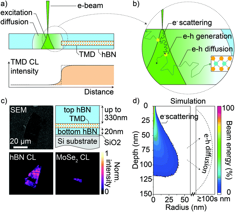 | ||
| Fig. 1 (a) Top: Sketch of the cross-sectional side view of a TMDC ML encapsulated in hBN. The interaction volume of the incident electrons is in dark green and the charge carrier diffusive zone is in lighter green. Bottom: Sketch plot of the intensity of the CL signal as a function of the e-beam position across the TMDC edge (TMDC CL edge response). The dashed step function is the ideal profile of a perfect probe, while the orange smooth sigmoid depicts the broadening of the edge response in the presence of electron and exciton diffusion. (b) Detailed view of the circled region in (a). The cartoon highlights the random path of an incident electron as a consequence of multiple electron scattering events; one of these events is shown to generate an e–h pair or exciton that diffuses beyond the electron interaction volume and can excite the TMDC, even though the e-beam does not directly interact with it. (c) Counterclockwise order from upper left: 3 kV scanning electron micrograph, hBN CL (>3.032 eV), and MoSe2 CL (<1.687 eV) maps at 20 K and cross-section scheme of a typical sample. (d) Cross-sectional view of the radially-averaged energy deposition by a 3 kV e-beam in hBN, according to a Monte Carlo simulation using the software CASINO.41 The dashed line is indicative of the range of exciton diffusion, exceeding several times the electron interaction volume. | ||
We note that the high charge-carrier binding energy in hBN32,45 suggests that e–h pairs form tightly bound excitons. The e–h pair or exciton diffusion volume is schematically indicated by the light green area in Fig. 1a.
Fig. 1b shows a zoomed-in representation of the events of electron scattering in the electron interaction volume, including e–h generation and the subsequent diffusion process up to the TMDC interface. It is of specific interest in our study that diffusive excitons can reach the TMDC even if the e-beam is still far from the TMDC edge. We note that due to the lower TMDC bandgap, it acts as an efficient sink for the excitons reaching the interface, leading to exciton generation inside the TMDC. The radiative recombination of the excitons is then used as a probe to quantitatively monitor the amount of excitons reaching the interface, where exciton diffusion in the TMDC itself can be neglected due to their lifetimes being limited to a few picoseconds by fast radiative decay at low temperatures.46–48 Therefore, there are three contributions, as shown in Fig. 1a and b, that define the effective finite size of the probe and thus the resolution of CL: the size of the focused e-beam, the electron interaction volume, and the diffusion volume. In this work, we demonstrate that the length scale of exciton diffusion in hBN exceeds the size of the e-beam and the electron interaction volume by at least an order of magnitude, making it by far the dominating factor in determining the spatial resolution of CL of hBN-encapsulated TMDCs.
Fig. 1c shows an SEM image of a typical hBN-encapsulated sample. The general sample configuration is shown in the sketch at the upper right corner of Fig. 1c. A silicon substrate with ∼2 nm of native oxide is used to limit the charging effect during the CL scans. At the bottom in Fig. 1c, we report the hBN and MoSe2 CL emission at 20 K (energies above 3.032 eV and below 1.687 eV, respectively) from the same scan. The hBN band-edge emission is strongly quenched in the presence of the MoSe2 flake. This confirms a very efficient transfer of excitons from the hBN to the TMDC, which is the working principle of TMDC CL valid across all TMDC materials. At the same time, the bright signal from both the hBN and the TMDC, suggests that possible non-radiative recombination at the hBN surface or at the interface is dominated by the radiative recombination rate in both the hBN and the TMDC.
Fig. 1d shows a cross-sectional view of the energy that the incident electrons retain as a function of their position in hBN. The view sums all the contributions along the direction perpendicular to the cross-section plane. We obtained this result by a Monte Carlo simulation of one million electrons at a 3 kV acceleration voltage using the software CASINO.42 The incident electrons deposit 95% of their energy in hBN within a 46 nm radius around the incident spot and a depth of 128 nm from the surface. We use these dimensions to define the electron interaction volume,38 although Fig. 1d clarifies that the e-beam deposits most of its energy in a smaller volume on the order of 10 nm. The dashed line already qualitatively indicates that the exciton diffusion length can easily exceed the size of the electron interaction volume, depending on the hBN thickness. This dependence of the hBN exciton diffusion length is discussed in detail in the following section.
Effect of hBN thickness on the spatial resolution in cathodoluminescence
In this study, we focused on low-temperature CL because several TMDC excitonic complexes, not observed at room temperature, appear and become spatially localized. Yet, we have confirmed that the CL edge response on the same samples used here are identical at room temperature (see section S12 in the ESI for details†). Fig. 2b shows a CL map of an MoSe2 ML fully encapsulated in hBN. The white dashed lines are a guide to the eye of the ML edges. The total thickness of 43 ± 2 nm was obtained by atomic force microscopy (AFM, see section S5 in the ESI for illustrative AFM profiles†).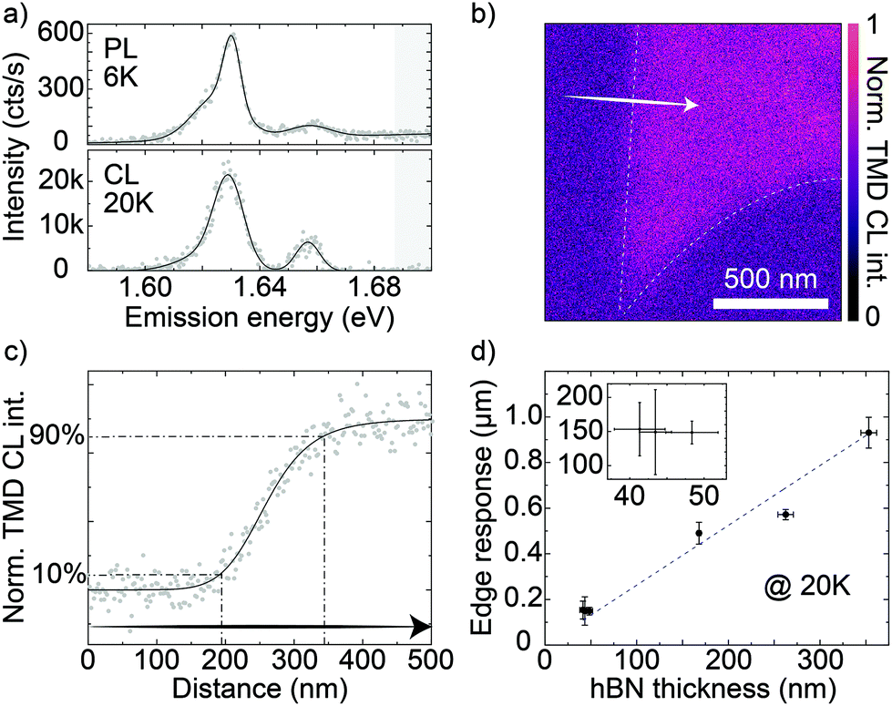 | ||
| Fig. 2 (a) PL (top) and CL (bottom) spectra of hBN-encapsulated MoSe2 MLs at 6 K and 20 K, respectively. The solid lines are Gaussian fits to data. The gray bands show the wavelengths discarded by a long-pass filter (edge at 1.687 eV) used for MoSe2 imaging. (b) Normalized CL intensity raster scan of MoSe2 ML encapsulated in 43 ± 2 nm of hBN. The dashed white lines are a guide to the eye of the MoSe2 flake edges derived from the TMDC CL map. (c) CL intensity vs position along the arrow in (b). The solid line is a logistic fit to the data. The dashed-dotted lines mark the 10–90% intensity range used to measure the edge response. (d) Average values of the MoSe2 CL edge response as a function of the total hBN thickness. The inset zooms into an interval of thinner hBN. The error bars are the standard deviation of the data sets; the dashed line is a linear fit to the data. | ||
We acquired the TMDC signal at 20 K by means of a photomultiplier tube (PMT) and selectively detected only the MoSe2 emission using a long-pass filter. We show illustrative micro-PL and CL spectra of the MoSe2 emission at low temperature in Fig. 2a. The two techniques show very similar emission peaks, with only minor differences due to the specific position within the same ML at which the spectra were acquired. The cut-off wavelength is indicated by the gray area in the spectra in Fig. 2a (we discuss peak assignment in more detail in the last section). We prepared multiple MoSe2 ML samples fully encapsulated in hBN with varying thicknesses of the top hBN layer. The edge response was extracted at multiple different positions in each CL map of MoSe2 MLs acquired with an acceleration voltage of 3 kV. To better study the effect of the hBN thickness, we limit this work to CL maps acquired at 3 kV. Moreover, we observe that changing the electron acceleration voltage has a negligible role in controlling the edge response (section S7 in the ESI†).
Fig. 2c reports a prototypical edge response (gray dots) corresponding to a line scan along the white arrow in Fig. 2b. In order to obtain a metric for the TMDC CL spatial resolution, we measured the width of the edge response as the distance between the two positions where CL intensity is 10% and 90% of the amplitude A, as obtained from the fit of each curve with the function:
We also measured the secondary electron (SE) edge response of our microscope using a 3 kV electron beam as a function of hBN thickness (section S6 in the ESI†). We observed that the SE response increases in thicker hBN layers, but it is always at least one order of magnitude smaller than the CL edge response. Therefore, the SE edge response is largely negligible in contributing to the CL edge response at a given hBN thickness.
Effective exciton diffusion length in hBN after e-beam excitation
We now turn to a method to measure the exciton diffusion length in hBN, which is inherently linked to the width of the CL edge response. As previously mentioned, we assume that (1) MoSe2 is a perfect sink for mobile carriers in hBN and (2) the radiative transfer rate at the MoSe2 layer is significantly higher than the non-radiative recombination rate at the hBN surface. This assumption is supported by the strong quenching of the hBN luminescence on top of the TMDC (Fig. 1c). It also suggests that most excitons cannot travel a long distance in the hBN on top of the TMDC: therefore, while the probe approaches the TMDC, we can simply assume that the majority of the exciton transfer happens near the TMDC edge. Under these assumptions, the intensity of the MoSe2 emission is proportional to the exciton concentration reaching the ML and the spatial distribution of excitons directly depends on their diffusion in the hBN layer. Among different experimental strategies to measure charge-carrier diffusion lengths by a scanning probe,49–51 our experimental configuration facilitates the implementation of a simple method based on measuring how steeply the CL signal rises while the probe approaches the sharp onset of a light emitter.50 The density of excitons decreases with increasing distance from the electron interaction volume; therefore, while the e-beam approaches the TMDC, an increasingly larger number of excitons can reach and excite the TMDC. A steep increase in the response indicates short diffusion lengths while a more gradual increase is indicative of dominant contributions from diffusion with longer average diffusion lengths. Importantly, this method measures the exciton diffusion in hBN regardless of the consequent diffusion inside the TMDC. Under a wide range of experimental conditions, the spatial profile of the luminescence intensity due to diffusive charge carriers is well described by an exponential function49–51 derived by Fick's law in the form:| y0 + Aex/Lxy |
We performed our analysis on the same data set used in Fig. 2. The inset in Fig. 3a shows the same experimental curve also presented in Fig. 2c. The dashed line goes through the inflection point of the curve logistic fit, that we use as a systematic definition of the position of the MoSe2 edge which is not visible by SEM imaging during the CL acquisitions. The main graph in Fig. 3a presents the lower part of the curve together with its exponential fit (solid curve) to obtain the parameter Lxy. Through the same procedure, we extracted the diffusion length Lxy as a function of the hBN thickness for all measurements shown in Fig. 2d, as presented in Fig. 3b. The graph shows that the in-plane diffusion length Lxy increases linearly with an increasing hBN thickness; interestingly, the slope of the linear fit (dashed line in Fig. 3b) is almost one (0.91 ± 0.02 nm), suggesting an increase of 1 nm in thickness corresponds to an increase of about 1 nm in Lxy.
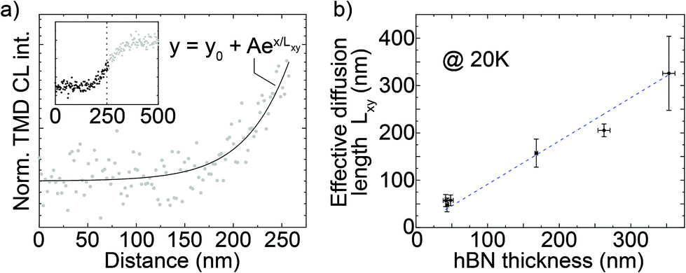 | ||
| Fig. 3 (a) Onset of the CL intensity edge response as a function of hBN thickness from Fig. 2c (reported in the inset). The dots are experimental data, the line is the exponential fit to the data according to the equation in the plot. (b) Average values of the effective diffusion length Lxy derived from exponential fit like in (a) as a function of the total hBN thickness. The error bars are the standard deviations of the data. | ||
All data in Fig. 3 are shown for the 20 K measurements, but room-temperature data lead to similar results and in particular an almost identical one-to-one linear relation of Lxy and hBN thickness (see sections S12 and S13 in ESI†). This diffusion-thickness correlation is analogous to the resolution-thickness correlation of Fig. 2 and corroborates the hypothesis that the hBN thickness controls the CL spatial resolution by limiting exciton diffusion.
Moreover, the negligible change in edge response in thick hBN as a function of the acceleration voltage (S7 in the ESI†) suggests that exciton diffusion controls the edge response rather than the acceleration voltage. This observation supports that we can neglect the effect of the voltage-dependent size of injection volume for determining the diffusion volume.
To give an intuitive interpretation for the behavior of spatial resolution and diffusion as a function of the hBN thickness, we consider the out-of-plane Lz and in-plane Lxy components of the exciton diffusion length in hBN. Their vectorial sum gives the total three-dimensional diffusion length Ltot. We do not have direct access to this total diffusion length; yet, we know that the fundamental limit for the out of plane diffusion is simply given by the layer thickness of the hBN. In general, we do not observe a significant decrease of CL intensity when the hBN is thicker than the depth of the electron interaction volume (data not shown). We thus infer that the majority of the excitons can diffuse deep enough from the electron interaction volume to reach the TMDC layer, at least in the investigated thickness range. This suggests that the diffusion length is larger than the distance between the interaction volume and the TMDC even in the thickest sample, setting a lower limit to the diffusion length. Since the thickest top hBN is 340 ± 8 nm and we calculate that 95% of electron energy is lost within 128 nm from the hBN surface, we can therefore estimate that the exciton diffusion length in hBN is at least 212 ± 8 nm in the out-of-plane direction.
With the out of plane diffusion length thus given by the hBN thickness, we can take a very simple approximation, where the linear, almost one-to-one behavior of hBN thickness (=Lz) and Lxy then suggest that excitons in hBN diffuse with very similar efficiencies in the in-plane and out-of-plane directions. We note that this analysis does not take into account the anisotropic electron injection profile. Given the layered nature of the material, indications for almost isotropic exciton diffusion constitutes an intriguing observation.
Optimization of CL intensity by varying hBN thickness
We now focus on the control of the CL brightness. While a more general discussion is available in section S10 the ESI,† here we focus on factors that we can control through the hBN thickness: the fluence G of excitons generated in hBN, and the coefficient of absorption fA and reflection and fR that affect the transmission of the light emitted by the buried TMDC, so that the CL intensity, ICL ∼ GfAfR.G directly scales with the fraction of the e-beam energy deposited into hBN: if the hBN is thinner than the electron interaction volume in bulk hBN, part of the e-beam energy is lost and cannot generate excitons in hBN.
Fig. 4a shows the percentage of energy released from a 3 kV e-beam into hBN as a function of the increasing hBN thickness (Monte Carlo CASINO42 simulations of 1 million electrons): the curve increases almost linearly from 0% to 100% with increasing hBN thickness until about 130 nm where it plateaus. Therefore, for a given e-beam energy, we can set the excitation power by changing the hBN thickness; conversely, for a given hBN thickness, we can tune the e-beam acceleration to control the energy proportion deposited in hBN. Simulations on the energy absorption as a function of the e-beam acceleration are available in section S7 in the ESI.† Using three-dimensional finite-difference time-domain Lumerical simulations (details in section S11 in the ESI†), we also calculate the transmission of light across the top hBN layer of hBN–MoSe2–hBN structures on Si substrates, which we show in the contour plot in Fig. 4b as a function of wavelength and top hBN thickness (bottom hBN at a constant thickness of 20 nm). At the emission energies of the MoSe2 room- and low-temperature luminescence (1.568 eV and 1.658 eV, respectively, marked by the dashed lines in Fig. 4b) the first transmission maxima happen for a top hBN thickness of about 104 nm and 93 nm, respectively.
 | ||
| Fig. 4 (a) Energy deposited in hBN by a 3 kV e-beam as a function of the hBN thickness (Monte Carlo simulations). 100% corresponds to the whole e-beam energy deposited in hBN. (b) Three-dimensional Lumerical simulation of light transmission through top hBN as a function of the top hBN thickness between 10 nm and 500 nm (bottom hBN fixed at 20 nm). (c) Right axis: Transmission at 1.658 eV from the simulation in (b) as a function of the total hBN thickness (top and bottom). Left axis: CL intensity as a function of total hBN thickness obtained combining the curve in (a) with the transmission at 1.658 eV. (d) Inset: CL intensity from (c) (right axis) and the inverse of the edge response (left axis). Main: CL intensity from (c) divided by the edge response (linear fit in Fig. 2d) as a function of the total hBN thickness (bottom axis) and edge response (top axis). The blue shadowing indicates the range of optimization for brightness and resolution. | ||
In Fig. 4c (right Y axis) we show the transmission coefficient at 1.658 eV extracted from Fig. 4b as a function of the total (top and bottom) hBN thickness. We then multiply this transmission coefficient by the curve in Fig. 4a to obtain the intensity factor ICL ∼ fAfRG. On the left axis of Fig. 4c, we report ICL as a function of the total hBN thickness. From the curve in Fig. 4c, we observe that increasing the total hBN thickness increases the CL brightness up to about 125 nm. For thicker hBN, Fig. 4c shows a slightly modulated, almost constant intensity.
On the contrary, we observed in Fig. 2d that the CL spatial resolution decreases with increasing hBN thickness. We highlight the opposing behavior of brightness and resolution vs. hBN thickness in the inset in Fig. 4d where we report the product of ICL ∼ fAfRG and 1/Δ (where Δ is the edge response fit from Fig. 2d) as a function of the total hBN thickness. In the main graph in Fig. 4d, we multiply the two curves in the inset to obtain ICL/Δ. The dashed part of the curve indicates an extrapolation beyond experimental data. ICL/Δ is a concise metric of the CL brightness normalized by resolution, which helps visualize that a practical trade-off between brightness and resolution is achievable up to about 100 nm of total hBN; beyond this value, the CL intensity only slightly increases, while the spatial resolution quickly worsens into values easily achieved by diffraction-limited optical microscopy. The blue shading in Fig. 4d indicates the resulting optimal range of hBN thickness. Generally, for an increase of signal intensity a value close to 100 nm should be chosen, whereas smaller values of hBN thicknesses result in lower CL intensity but spatial higher resolution: for instance, with 40 nm of hBN the edge response is as narrow as 104 nm (top axis in Fig. 4d), but the TMDC CL intensity decreases to 25% of the maximum. This metric can be adapted for any given system and the top layer thickness can then be adjusted to the experimental needs. We derived similar conclusions also from room-temperature measurements, shown in section S14 in the ESI.†
Hyperspectral maps reveal complex heterogeneity resolved beyond the diffusion-limited spatial resolution
We now turn to CL hyperspectral maps where we show that locally and spectrally separable emission features can help to improve resolution below the exciton diffusion limit. Fig. 5a is a 20 K hyperspectral CL map of the emission (1.569 eV to 1.675 eV shown) from MoSe2 ML encapsulated in total 263 ± 9 nm of hBN. The ML is to the right of the dashed line. The map shows significant variations of the intensity of the MoSe2 emission at different sub-micron length scales. In Fig. 5b, we show a plot of the emission spectra along the horizontal black arrow in Fig. 5a, covering more than 3 μm from beyond the MoSe2 edge into the flake, with observed variations in both emission energy and intensity. Fig. 5c shows three normalized spectra I, II, and III from positions indicated by the dashed lines in Fig. 5b. By fitting the low-energy peak, we observe a redshift of about 15 meV, from 1.609 eV to 1.594 eV, between the spectra I and III. At the same time, the peak maintains a similar FWHM of slightly less than 9 meV. The high-energy peak is spectrally stable at 1.635 eV, with a FWHM of about 8 meV in spectrum I and a slight broadening towards the MoSe2 edge (not shown in Fig. 5c, but already visible in the plot in Fig. 5b). By comparison with literature and with the support of temperature-dependent CL spectra (shown in section S15 in the ESI†), the high-energy peak matches the neutral MoSe2 exciton emission whereas the low-energy one would match the reported energy range of charged exciton emission.52,53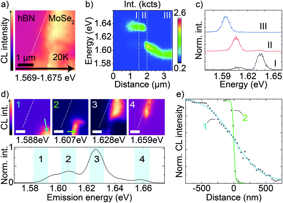 | ||
| Fig. 5 (a) Hyperspectral CL map of a MoSe2 ML encapsulated in hBN of total thickness of 263 ± 9 nm over the energy range of 1.569–1.675 eV obtained at 20 K. The white dashed line indicates the MoSe2 edge. (b) Plot of the spectra along the black arrow in (a). (c) CL spectra extracted from (b) at the positions I, II, III indicated by the vertical dashed lines. (d) Same hyperspectral map as in (a) that shows intensity within narrower 10 meV bands centered at 1.588 eV (1), 1.607 eV (2), 1.628 eV (3), and 1.659 eV (4) indicated by blue shadowing in the bottom spectrum of the whole map emission. The scale bars are 1 μm. (e) Normalized CL intensity as a function of distance along the green arrows in the maps 1 and 2 in (d) together with logistic fit (solid lines). Data offset to center the inflection points. | ||
In the lower panel in Fig. 5d, we show the normalized emission spectrum from the whole map in Fig. 5a. Together with the two peaks assigned to the neutral and charged excitons of MoSe2, here further peaks are visible. Although we do not study the origin of these peaks, they may be associated with excitonic complexes affected by spectral shifts in different positions of the map due to local structural defects or strain, as reported in similar TMDC systems.36,54 In the spectrum in Fig. 5d, the blue bands highlight the four 10 meV-wide energy bands that we show in the four top panels in Fig. 5d. These bands are centered at 1.588 eV (1), 1.607 eV (2), 1.628 eV (3), and 1.659 eV (4).
The corresponding four maps show that different emission peaks dominate spatially distinct sub-micron regions. Fig. 5e shows the intensity profile along the short green lines in Fig. 5d (1) and (2). These intensity profiles are directly obtained from the spectrally filtered hyperspectral maps in (1) and (2). By the same logistic fit used for the edge responses of Fig. 2 (solid lines in Fig. 5e) we obtain an edge response of 936 ± 27 nm and 54 ± 6 nm for the lines in (1) and (2), respectively. The first edge is comparable to the average edge response measured in Fig. 2 (about 600 nm) for a sample of this hBN thickness, but the second edge is one order of magnitude narrower than the expected edge response. We believe that this effect is due to the presence of a highly localized emission, which we can distinguish it from the surroundings by a narrow spectral selection.12,55 This is similar to implementations of super-resolution microscopy in optics and similar to other reports of highly-resolved TMDC CL.36 In the same flake, we observe even narrower features (edge response of 27 nm in section S16 of the ESI†) as well as wider ones, like edge (1). The enhancement of spatial resolution through spectral filtering of hyperspectral maps offers an additional degree of freedom to enhance the resolution together with the reduction of the hBN thickness that we have discussed in the previous sections. To discern what phenomena account for the observed formation,56 localization,53 or energy shift30,57 of specific emission peaks in our sample, dedicated experiments (like morphological correlations, control of the Fermi level, etc.) are necessary and are beyond the scope of our current discussion. In this section we have highlighted how spectrally resolved CL mapping can be utilized to achieve truly nanoscale imaging despite otherwise longer diffusion-limited resolution.
Conclusions
In conclusion, we have demonstrated the optimization of cathodoluminescence microscopy of buried interfaces through nanoscale heterostructure design. We focused on prototypical hBN encapsulated monolayer TMDC systems and delineated the prominent role of exciton diffusion in hBN to define the spatial resolution of CL. Surprisingly this diffusion was found to be nearly isotropic and we determined for the first time the out-of-plane hBN exciton diffusion length to be >200 nm. We find that the spatial resolution monotonically decreases for increasing hBN thicknesses and we correlate this observation with the associated linear increase of the in-plane diffusion length in thicker hBN. This observation will enable a deeper understanding of charge-carrier phenomena in hBN, such as exciton annihilation.38 We further demonstrated that the thickness of the hBN encapsulation is an easily tunable parameter that allows us to control the brightness of the TMDC CL signal. We combine our study of CL resolution and brightness to define a practical range of hBN thicknesses below 100 nm within which thicker layers favor a brighter emission and thinner ones enhance the spatial resolution at the expense of the signal intensity.Finally, we show that we can leverage hyperspectral CL maps to resolve spectrally distinct nanoscale features beyond the spatial resolution set by the diffusion of carriers. The use of hBN as an indirect excitation medium is generalizable to other nanoscale semiconductors, beyond the prototypical case study of TMDC MLs. We envision hBN-mediated CL as a flexible characterization technique that can also benefit delicate, beam-sensitive structures.
Experimental
Sample preparation
All the samples used in this manuscript were obtained by successive picking-up of exfoliated hBN and TMDC MLs using a PC film and subsequent stamping onto Si substrates, followed by cleaning in CHCl3 for few hours, rinsing in isopropyl alcohol and drying under a gentle nitrogen flux.We adjusted the acquisition times in each map to ensure that the signal clearly overcomes the detector noise. However, we observed that an increasing noise level simply degrades the quality of the logistic fit but does not introduce any systematic error towards either the narrowing or broadening of the fit-derived width of the edge response (demonstrated by simulations reported in section S9 in the ESI†). We also kept the e-beam current at 197 pA to keep the concentration of the charge carriers generated in hBN low. Large charge-carrier concentrations would lead to significant exciton–exciton annihilation, also known as Auger recombination. However, from the work by Plaud et al.,38 we infer that current values below 200 pA largely mitigate Auger effects. These processes would otherwise lead to the loss of excitons that would not contribute to the CL emission and may also affect the diffusion dynamics by shortening the charge-carrier lifetimes.38
While measuring the CL edge response, we used a density of pixels high enough to ensure that they do not limit the CL spatial resolution; that is, the pixel size is several times smaller than the edge response width.
Author contributions
LF, AR: conceptualization. JC, SS: sample fabrication. LF: data acquisition, curation and analysis. AR: project supervision. LF prepared the first draft with inputs from JC, JZ, AR. LF, JZ, SS, FR, DB, SA, DFO, AR revised the manuscript. All co-authors have approved the final draft.Conflicts of interest
There are no conflicts to declare.Acknowledgements
All authors would like to thank Dr Sunphil Kim for his contribution to sample preparation and for fruitful discussions. Work at the Molecular Foundry (including sample preparation, CL and PL measurements, and AFM maps) was supported by the Office of Science, Office of Basic Energy Sciences, of the U.S. Department of Energy under Contract No. DE-AC02-05CH11231. A. R. acknowledges support through the Early Career LDRD Program of Lawrence Berkeley National Laboratory under DOE Contract No. DE-AC02-05CH11231. L. F. acknowledges funding from the Swiss National Science Foundation (SNSF) via Early PostDoc Mobility Grant No. P2ELP2_184398. J. Z. acknowledges funding by the Deutsche Forschungsgemeinschaft (DFG, German Research Foundation) through the Walter-Benjamin Programme 462503440, and the U.S. Department of Energy, Office of Science, Basic Energy Sciences, Materials Sciences and Engineering Division, award number DE-SC0022289. D. B. acknowledges support from the U.S. Department of Energy, Office of Science, Office of Workforce Development for Teachers and Scientists, Office of Science Graduate Student program through the SCGSR program administered by the Oak Ridge Institute for Science and Education (ORISE) for the DOE. ORISE is managed by ORAU under contract number DE-SC0014664. K. W. and T. T. acknowledge support from JSPS KAKENHI (Grant Numbers 19H05790, 20H00354 and 21H05233).Notes and references
- A. K. Geim and I. V. Grigorieva, Nature, 2013, 499, 419–425 CrossRef CAS PubMed.
- J. Holler, L. Bauriedl, T. Korn, A. Seitz, F. Özyigit, M. Eichinger, C. Schüller, K. Watanabe, T. Taniguchi, C. Strunk and N. Paradiso, 2D Mater., 2019, 7, 015012 CrossRef.
- M. Seitz, P. Gant, A. Castellanos-Gomez and F. Prins, Nanomaterials, 2019, 9, 1120 CrossRef CAS PubMed.
- M. I. B. Utama, H. Kleemann, W. Zhao, C. S. Ong, F. H. da Jornada, D. Y. Qiu, H. Cai, H. Li, R. Kou, S. Zhao, S. Wang, K. Watanabe, T. Taniguchi, S. Tongay, A. Zettl, S. G. Louie and F. Wang, Nat. Electron., 2019, 2, 60–65 CrossRef CAS.
- D. Rhodes, S. H. Chae, R. Ribeiro-Palau and J. Hone, Nat. Mater., 2019, 18, 541–549 CrossRef CAS PubMed.
- A. Raja, L. Waldecker, J. Zipfel, Y. Cho, S. Brem, J. D. Ziegler, M. Kulig, T. Taniguchi, K. Watanabe, E. Malic, T. F. Heinz, T. C. Berkelbach and A. Chernikov, Nat. Nanotechnol., 2019, 14, 832–837 CrossRef CAS PubMed.
- C. F. Klingshirn, Semiconductor Optics, Springer Science & Business Media, 2007 Search PubMed.
- G. Remond, F. Cesbron, R. Chapoulie, D. Ohnenstetter, C. Roques-Carmes and M. Schvoerer, Scanning Microsc., 1992, 6, 2 Search PubMed.
- A. K. Chin, C. L. Zipfel, S. Mahajan, F. Ermanis and M. A. DiGiuseppe, Appl. Phys. Lett., 1982, 41, 555–557 CrossRef CAS.
- J. T. Griffiths, S. Zhang, B. Rouet-Leduc, W. Y. Fu, A. Bao, D. Zhu, D. J. Wallis, A. Howkins, I. Boyd, D. Stowe, M. J. Kappers, C. J. Humphreys and R. A. Oliver, Nano Lett., 2015, 15, 7639–7643 CrossRef CAS PubMed.
- N. Bologna, S. Wirths, L. Francaviglia, M. Campanini, H. Schmid, V. Theofylaktopoulos, K. E. Moselund, A. F. I. Morral, R. Erni, H. Riel and M. D. Rossell, ACS Appl. Mater. Interfaces, 2018, 10, 32588–32596 CrossRef CAS PubMed.
- L. Francaviglia, G. Tütüncüoglu, F. Matteini and A. F. I. Morral, Nanotechnology, 2019, 30, 054006 CrossRef CAS PubMed.
- F. J. García de Abajo, Rev. Mod. Phys., 2010, 82, 209–275 CrossRef.
- A. Splendiani, L. Sun, Y. Zhang, T. Li, J. Kim, C.-Y. Chim, G. Galli and F. Wang, Nano Lett., 2010, 10, 1271–1275 CrossRef CAS PubMed.
- K. F. Mak, C. Lee, J. Hone, J. Shan and T. F. Heinz, Phys. Rev. Lett., 2010, 105, 136805 CrossRef PubMed.
- N. Kumar, J. He, D. He, Y. Wang and H. Zhao, Nanoscale, 2014, 6, 12690–12695 RSC.
- J. Krustok, T. Raadik, R. Jaaniso, V. Kiisk, I. Sildos, M. Marandi, H.-P. Komsa, B. Li, X. Zhang, Y. Gong and P. M. Ajayan, Appl. Phys. Lett., 2016, 109, 253106 CrossRef.
- L.-N. Nguyen, Y.-W. Lan, J.-H. Chen, T.-R. Chang, Y.-L. Zhong, H.-T. Jeng, L.-J. Li and C.-D. Chen, Nano Lett., 2014, 14, 2381–2386 CrossRef CAS PubMed.
- F. Withers, O. Del Pozo-Zamudio, A. Mishchenko, A. P. Rooney, A. Gholinia, K. Watanabe, T. Taniguchi, S. J. Haigh, A. K. Geim, A. I. Tartakovskii and K. S. Novoselov, Nat. Mater., 2015, 14, 301–306 CrossRef CAS PubMed.
- A. Chaves, J. G. Azadani, H. Alsalman, D. R. da Costa, R. Frisenda, A. J. Chaves, S. H. Song, Y. D. Kim, D. He, J. Zhou, A. Castellanos-Gomez, F. M. Peeters, Z. Liu, C. L. Hinkle, S.-H. Oh, P. D. Ye, S. J. Koester, Y. H. Lee, P. Avouris, X. Wang and T. Low, npj 2D Mater. Appl., 2020, 4, 1–21 CrossRef.
- P. Rivera, J. R. Schaibley, A. M. Jones, J. S. Ross, S. Wu, G. Aivazian, P. Klement, K. Seyler, G. Clark, N. J. Ghimire, J. Yan, D. G. Mandrus, W. Yao and X. Xu, Nat. Commun., 2015, 6, 6242 CrossRef CAS PubMed.
- C. Jin, E. C. Regan, D. Wang, M. Iqbal Bakti Utama, C.-S. Yang, J. Cain, Y. Qin, Y. Shen, Z. Zheng, K. Watanabe, T. Taniguchi, S. Tongay, A. Zettl and F. Wang, Nat. Phys., 2019, 15, 1140–1144 Search PubMed.
- E. C. Regan, D. Wang, C. Jin, M. Iqbal Bakti Utama, B. Gao, X. Wei, S. Zhao, W. Zhao, Z. Zhang, K. Yumigeta, M. Blei, J. D. Carlström, K. Watanabe, T. Taniguchi, S. Tongay, M. Crommie, A. Zettl and F. Wang, Nature, 2020, 579, 359–363 CrossRef CAS PubMed.
- H.-H. Fang, J. Yang, S. Tao, S. Adjokatse, M. E. Kamminga, J. Ye, G. R. Blake, J. Even and M. A. Loi, Adv. Funct. Mater., 2018, 28, 1800305 CrossRef.
- M. Shanmugam, R. Jacobs-Gedrim, C. Durcan and B. Yu, Nanoscale, 2013, 5, 11275–11282 RSC.
- V. Raj, D. Chugh, L. E. Black, M. M. Shehata, L. Li, F. Kremer, D. H. Macdonald, H. H. Tan and C. Jagadish, npj 2D Mater. Appl., 2021, 5, 1–8 CrossRef.
- E. Courtade, M. Semina, M. Manca, M. M. Glazov, C. Robert, F. Cadiz, G. Wang, T. Taniguchi, K. Watanabe, M. Pierre, W. Escoffier, E. L. Ivchenko, P. Renucci, X. Marie, T. Amand and B. Urbaszek, Phys. Rev. B, 2017, 96, 085302 CrossRef.
- F. Cadiz, E. Courtade, C. Robert, G. Wang, Y. Shen, H. Cai, T. Taniguchi, K. Watanabe, H. Carrere, D. Lagarde, M. Manca, T. Amand, P. Renucci, S. Tongay, X. Marie and B. Urbaszek, Phys. Rev. X, 2017, 7, 021026 Search PubMed.
- A. Raja, A. Chaves, J. Yu, G. Arefe, H. M. Hill, A. F. Rigosi, T. C. Berkelbach, P. Nagler, C. Schüller, T. Korn, C. Nuckolls, J. Hone, L. E. Brus, T. F. Heinz, D. R. Reichman and A. Chernikov, Nat. Commun., 2017, 8, 15251 CrossRef PubMed.
- N. Peimyoo, H.-Y. Wu, J. Escolar, A. De Sanctis, G. Prando, F. Vollmer, F. Withers, A. C. Riis-Jensen, M. F. Craciun, K. S. Thygesen and S. Russo, ACS Appl. Mater. Interfaces, 2020, 12, 55134–55140 CrossRef CAS PubMed.
- M. Negri, L. Francaviglia, D. Dumcenco, M. Bosi, D. Kaplan, V. Swaminathan, G. Salviati, A. Kis, F. Fabbri and A. F. I. Morral, Nano Lett., 2020, 20, 567–576 CrossRef CAS PubMed.
- G. Cassabois, P. Valvin and B. Gil, Nat. Photonics, 2016, 10, 262–266 CrossRef CAS.
- G. Nayak, S. Lisi, W. L. Liu, T. Jakubczyk, P. Stepanov, F. Donatini, K. Watanabe, T. Taniguchi, A. Bid, J. Kasprzak, M. Richard, V. Bouchiat, J. Coraux, L. Marty, N. Bendiab and J. Renard, Phys. Rev. Mater., 2019, 3, 114001 CrossRef CAS.
- S. Zheng, J.-K. So, F. Liu, Z. Liu, N. Zheludev and H. J. Fan, Nano Lett., 2017, 17, 6475–6480 CrossRef CAS PubMed.
- A. Singh, H. Y. Lee and S. Gradečak, Nano Res., 2020, 13, 1363–1368 CrossRef CAS.
- N. Bonnet, H. Y. Lee, F. Shao, S. Y. Woo, J.-D. Blazit, K. Watanabe, T. Taniguchi, A. Zobelli, O. Stéphan, M. Kociak, S. Gradečak and L. H. G. Tizei, Nano Lett., 2021, 21, 10178–10185 CrossRef CAS PubMed.
- P. R. Edwards and R. W. Martin, Semicond. Sci. Technol., 2011, 26, 064005 CrossRef.
- A. Plaud, L. Schué, K. Watanabe, T. Taniguchi, F. Fossard, F. Ducastelle, A. Loiseau and J. Barjon, Appl. Phys. Lett., 2019, 114, 232103 CrossRef.
- S. W. Hell and J. Wichmann, Opt. Lett., 1994, 19, 780–782 CrossRef CAS PubMed.
- E. Betzig, G. H. Patterson, R. Sougrat, O. W. Lindwasser, S. Olenych, J. S. Bonifacino, M. W. Davidson, J. Lippincott-Schwartz and H. F. Hess, Science, 2006, 313, 1642–1645 CrossRef CAS PubMed.
- M. J. Rust, M. Bates and X. Zhuang, Nat. Methods, 2006, 3, 793–795 CrossRef CAS PubMed.
- D. Drouin, A. R. Couture, D. Joly, X. Tastet, V. Aimez and R. Gauvin, Scanning, 2007, 29, 92–101 CrossRef CAS PubMed.
- J. R. Michael and D. B. Williams, J. Microsc., 1987, 147, 289–303 CrossRef.
- J. Kološová, T. Hrnčíř, J. Jiruše, M. Rudolf and J. Zlámal, Microsc. Microanal., 2015, 21, 206–211 CrossRef.
- P. Jaffrennou, J. Barjon, J.-S. Lauret, B. Attal-Trétout, F. Ducastelle and A. Loiseau, J. Appl. Phys., 2007, 102, 116102 CrossRef.
- M. Palummo, M. Bernardi and J. C. Grossman, Nano Lett., 2015, 15, 2794–2800 CrossRef CAS PubMed.
- C. Robert, D. Lagarde, F. Cadiz, G. Wang, B. Lassagne, T. Amand, A. Balocchi, P. Renucci, S. Tongay, B. Urbaszek and X. Marie, Phys. Rev. B, 2016, 93, 205423 CrossRef.
- G. Moody, C. Kavir Dass, K. Hao, C.-H. Chen, L.-J. Li, A. Singh, K. Tran, G. Clark, X. Xu, G. Berghäuser, E. Malic, A. Knorr and X. Li, Nat. Commun., 2015, 6, 1–6 Search PubMed.
- H. A. Zarem, P. C. Sercel, J. A. Lebens, L. E. Eng, A. Yariv and K. J. Vahala, Appl. Phys. Lett., 1989, 55, 1647–1649 CrossRef CAS.
- A. Gustafsson, J. Bolinsson, N. Sköld and L. Samuelson, Appl. Phys. Lett., 2010, 97, 072114 CrossRef.
- C.-H. Chu, M.-H. Mao, Y.-R. Lin and H.-H. Lin, Sci. Rep., 2020, 10, 5200 CrossRef CAS PubMed.
- G. D. Shepard, O. A. Ajayi, X. Li, X.-Y. Zhu, J. Hone and S. Strauf, 2D Mater., 2017, 4, 021019 CrossRef.
- T. Godde, D. Schmidt, J. Schmutzler, M. Aßmann, J. Debus, F. Withers, E. M. Alexeev, O. Del Pozo-Zamudio, O. V. Skrypka, K. S. Novoselov, M. Bayer and A. I. Tartakovskii, Phys. Rev. B, 2016, 94, 165301 CrossRef.
- A. Arora, N. K. Wessling, T. Deilmann, T. Reichenauer, P. Steeger, P. Kossacki, M. Potemski, S. M. de Vasconcellos, M. Rohlfing and R. Bratschitsch, Phys. Rev. B, 2020, 101, 241413(R) CrossRef.
- N. Kumar Balla, C. Rendón-Barraza, L. M. Hoang, P. Karpinski, E. Bermúdez-Ureña and S. Brasselet, ACS Photonics, 2017, 4, 292–301 CrossRef CAS.
- H.-P. Komsa, J. Kotakoski, S. Kurasch, O. Lehtinen, U. Kaiser and A. V. Krasheninnikov, Phys. Rev. Lett., 2012, 109(3), 035503 CrossRef PubMed.
- J. O. Island, A. Kuc, E. H. Diependaal, R. Bratschitsch, H. S. J. van der Zant, T. Heine and A. Castellanos-Gomez, Nanoscale, 2016, 8, 2589–2593 RSC.
Footnote |
| † Electronic supplementary information (ESI) available. See DOI: https://doi.org/10.1039/d1nr08082b |
| This journal is © The Royal Society of Chemistry 2022 |