
 Open Access Article
 This Open Access Article is licensed under a
 Creative Commons Attribution 3.0 Unported Licence
Defects in an orthorhombic MoAlB MAB phase thin film grown at moderate synthesis temperature†
Rajib
Sahu
 *ab,
Dimitri
Bogdanovski
b,
Jan-Ole
Achenbach
b,
Jochen M.
Schneider
ab and
Christina
Scheu
*ac
*ab,
Dimitri
Bogdanovski
b,
Jan-Ole
Achenbach
b,
Jochen M.
Schneider
ab and
Christina
Scheu
*ac
aMax-Planck-Institut für Eisenforschung GmbH, Max-Planck-Str. 1, 40237 Düsseldorf, Germany. E-mail: r.sahu@mpie.de; scheu@mpie.de
bMaterials Chemistry, RWTH Aachen University, Kopernikusstr. 10, 52074 Aachen, Germany
cMaterials Analytics, RWTH Aachen University, Kopernikusstr. 10, 52074 Aachen, Germany
First published on 2nd February 2022
Abstract
Here, we report on atomic scale characterization of various defects in a MoAlB (MAB) phase thin film grown by DC sputtering at a synthesis temperature of 700 °C. Aberration-corrected scanning transmission electron microscopy reveals the formation of an intergrown metastable Mo3Al2B4 phase accompanied by thermally stable 90° twist boundaries, coexisting within the pristine MoAlB matrix. The concurrent formation of these structural defects in the MoAlB matrix can be rationalized based on minute differences in formation enthalpies as shown via density functional theory calculations. The specific structural nature of both the twist boundary and compositional defect (Mo3Al2B4) in a MoAlB matrix is hitherto unreported in literature. Apart from these defects, faceted grain boundaries are observed. In the vicinity of amorphous AlOx regions, Al is deintercalated and a 2D MoB MBene phase is formed as reported before. Besides these amorphous AlOx regions, a few nanometer-sized 3D MoB clusters are found. The advancement of aberration-corrected scanning transmission electron microscopy significantly improves characterization from 1D to 3D defects which is important for thin film materials design for the moderate synthesis temperature range. The reported defects might play an important role in the formation of 2D MoB MBenes.
1. Introduction
Layered ternary transition metal borides such as MAB phases, where M is a transition metal, A a group III or VI element and B is boron, are known as ceramic nanolaminates.1,2 A specific class are Al-containing MAB phases which exist with several variable chemical formulas, such as MAlB, M2AlB2, M3AlB4, M4AlB6, and Mo7Al6B7.2,3 Unlike two-dimensional (2D) materials, where weak van der Waals interactions dominate the interlayer bonding, metallic M–Al interactions and strong covalent/ionic M–B bonds are present in MAB phases.4,5 Both the orthorhombic and hexagonal MoAlB MAB phases with an equistoichiometric 1![[thin space (1/6-em)]](https://www.rsc.org/images/entities/char_2009.gif) :1:1 composition are potential candidates for various applications such as protective coatings6,7 and battery electrodes.4,8–11 This is due to their good corrosion resistance,12 high temperature stability,12,13 and excellent electrical and thermal conductivities14etc. Typically, MoAlB MAB phases are synthesized at high temperatures of ∼1000–1400 °C in bulk form.4,8,9,12–16 Synthesizing orthorhombic MoAlB material at lower/moderate temperature is important for many industrial applications and at the same time challenging due to growth kinetics. Achenbach et al. reduced the growth temperature by 42% compared to the reported values and successfully synthesized a crystalline orthorhombic phase by direct current (DC) magnetron sputtering.7 Recently, Evertz et al. established that by adopting growth conditions that enable both surface and bulk diffusion, fully dense MoAlB coatings are grown.17 It is well known that plasma-assisted thin film deposition methods often lead to the formation of metastable phases,18,19 including a large number of defects of different dimensionalities.18,19,20–23
:1:1 composition are potential candidates for various applications such as protective coatings6,7 and battery electrodes.4,8–11 This is due to their good corrosion resistance,12 high temperature stability,12,13 and excellent electrical and thermal conductivities14etc. Typically, MoAlB MAB phases are synthesized at high temperatures of ∼1000–1400 °C in bulk form.4,8,9,12–16 Synthesizing orthorhombic MoAlB material at lower/moderate temperature is important for many industrial applications and at the same time challenging due to growth kinetics. Achenbach et al. reduced the growth temperature by 42% compared to the reported values and successfully synthesized a crystalline orthorhombic phase by direct current (DC) magnetron sputtering.7 Recently, Evertz et al. established that by adopting growth conditions that enable both surface and bulk diffusion, fully dense MoAlB coatings are grown.17 It is well known that plasma-assisted thin film deposition methods often lead to the formation of metastable phases,18,19 including a large number of defects of different dimensionalities.18,19,20–23
In the present work, we study various defects with different dimensionalities in an orthorhombic MoAlB MAB phase thin film grown at 700 °C by DC magnetron sputtering, using a combined experimental and computational approach. In contrast to the work of Achenbach et al.,7 a compound target was used for the deposition.24 The defects are characterized by different (scanning) transmission electron microscopy (S)TEM techniques including electron energy loss spectroscopy (EELS). The experiments reveal the presence of several defects, such as faceted grain boundaries, planar twist boundaries (TB), 3D intergrown compositional defects (CD) and amorphous clusters. The experimental findings can be correlated to the results of density functional theory (DFT) calculations, which predict comparable formation energies for the different defect types. Furthermore, the formation of MBene was observed in close vicinity of these defects, as reported earlier.24
2. Experimental
The MoAlB thin film was deposited using a single MoAlB compound target (from Plansee Composite materials GmbH, Germany) by DC magnetron sputtering, as described in detail in our previous work.24 The growth temperature was 700 °C and a single crystal Al2O3 (0001) was used as substrate. The final thickness of the coating was around ∼3 μm as measured on cross-sectional TEM micrographs (Fig. 1a). The average chemical composition ratios determined by time-of-flight energy elastic recoil detection analysis (ERDA) were Mo/Al = 0.96 and Mo/B = 0.85,24 indicating close-to-equistoichiometric composition. | ||
| Fig. 1 (a) Overview TEM micrograph of the MoAlB thin film cross section, showing a columnar growth with the long axis inclined to the substrate. (b) Cross-sectional bright field TEM micrograph revealing various defects, ranging from planar defects to 3D clusters, marked by red, white and black arrows. (c) Plan view HAADF STEM image of twist boundaries marked by white arrows. (d) SAD pattern of orthorhombic phase taken along [001] zone axis. | ||
Aberration-corrected STEM was conducted on a ThermoFisher probe-corrected Titan Themis while bright field imaging and selected area diffraction (SAD) were performed on an image-corrected Titan Themis. Both instruments were set at an accelerating voltage of 300 kV. Cross-sectional and plan view TEM samples were prepared and thinned down below 35 nm by conventional mechanical polishing and Ar ion milling in Gatan PIPS. A convergence angle of 23.8 mrad was chosen for high resolution STEM. A range of 10–16, 18–34, and 78–200 mrad was set as a collection angle for annular bright field (ABF), annular dark field (ADF) and high-angle annular dark field (HAADF) imaging, respectively. The EELS data were collected at 1 eV energy resolution measured from the full width at half maxima (FWHM) of the zero-loss peak. The spectra were acquired with a 2.5 nm aperture at an energy dispersion of 0.10 eV per channel. The microscope was equipped with a Bruker SuperX detector for energy-dispersive X-ray spectroscopy (EDX) analysis. The X-ray diffraction patterns were acquired with a Bruker D8 discovery general area detector diffraction system (GADDS) (Bruker, Billerica, MA, USA) using Cu(Kα) radiation.
3. Density functional theory
Energies of formation were obtained from density functional theory (DFT) calculations using the Vienna ab initio Simulation Package (VASP, version 5.4.4, University of Vienna, Austria).25–27 Projector-augmented waves (PAW)28 with a cut-off energy of 500 eV were used for basis set representation, with electron exchange and correlation treated via the generalized gradient approximation-based functional parametrized by Perdew, Burke and Ernzerhof (PBE).29 The Monkhorst–Pack method30 was employed to handle Brillouin zone integration, utilizing a smearing parameter of 0.15 eV and choosing a Γ-point-centered k-mesh of varying dimensions (depending on system size) to guarantee energetic convergence in each case. The valence electron configurations of the individual species as described in the utilized PAW potentials were 5s14d54p64s2 for Mo, 3s23p1 for Al and 2s22p1 for B.The initial structural model for MoAlB was taken from literature31 and fully optimized with respect to lattice parameters and atomic positions. As a subsequent energetic comparison of spin-polarized (ferromagnetic) and nonmagnetic MoAlB yielded identical results and zero magnetic moments for all atoms in the system in the spin-polarized case, spin polarization was not considered for any further calculations.
The defect-containing systems were modelled based on the experimental observations discussed in this work, with the goal of closely replicating the structural morphology of the defect in question, employing supercells. The resulting structural models, which were then fully optimized, are described in more detail in the discussion section. In the case of MoB, the previously optimized MoAlB structural model served as the starting point, with subsequent removal of the Al layer and full structural optimization.
The energy of formation in the ground state was obtained from the difference of the total energy of the system in question and the sum of the total energies of the corresponding elements in their ground states (body-centered cubic Mo, face-centered cubic Al, rhombohedral B), normalized to one mole:
| Ef = E0,DFT(MoxAlyBz) – (xE0,DFT(Mo) + yE0,DFT(Al) + zE0,DFT(B)) |
As all calculations were performed in the ground state at 0 K, we assume, neglecting pressure contributions, that ΔHf (0 K) ≈ ΔEf (0 K).
4. Results and discussion
Growth kinetics and energetics may induce several types of defects which can be used to design materials with specific properties, as discussed in prior literature.18,19 The overall microstructure of the as-deposited MoAlB thin film is displayed in Fig. 1(a) and is characteristic for columnar growth. Some seed crystals with a size of 10 to 30 nm are located at the film-substrate interface and are overgrown by columnar grains. Most of these elongated grains grow slightly inclined to the substrate normal (Fig. 1(b)). Their largest facet is typically parallel to the (020) plane and the longest axis parallel to the [100] direction, as depicted from the SAD pattern (Fig. (1d)). The SAD pattern also confirms that the MoAlB matrix possesses an orthorhombic crystal structure with lattice parameters in accordance with literature values (a = 3.18 Å, b = 14.12 Å and c = 3.12 Å).7 This is in agreement with X-ray diffraction data (ESI, Fig. S1†).Several defects are visible within the grains ranging from planar defects to 3D clusters (Fig. 1(b)). Two defects dominate: twist boundaries (TB) (marked with white arrows in Fig. 1(b) and (c)) and a novel, metastable compositional defect (CD) (red arrow in Fig. 1(b)). The domain width separated by the TB ranges up to 6 nm while the CD has a width less than 1 nm.
Before discussing the defects in detail, it is worth mentioning that two impurity phases are observed by STEM EDX, marked by white and yellow arrows in Fig. 2. This observation is consistent with our previous investigation of a MoAlB film deposited using two sputter targets.7 These impurity phases are Al- or O-rich and have an area fraction of 4.5% and 2%, respectively, while the remaining matrix regions are close to the ideal stoichiometric ratio in composition.24 We also observe formation of amorphous AlOx in the impurity regions, identified by yellow arrows in Fig. 2(d). The amorphous oxide is likely formed during synthesis due to incorporation of residual gases present within the sputtering chamber.32 In a recent work, we reported the concurrent formation of a MoAlB MAB phase and local two-dimensional MoB MBene in the vicinity of the AlOx region.24 The areal fraction of MoB MBene areas compared to all other impurity phases is <1% and the typical size of the amorphous AlOx region, where the MBene is formed, is ∼10×12 nm2.24 Basically, a three-component heterostructure consisting of MoAlB, MoB MBene and amorphous AlOx was identified, which indicated Al deintercalation from MoAlB.24
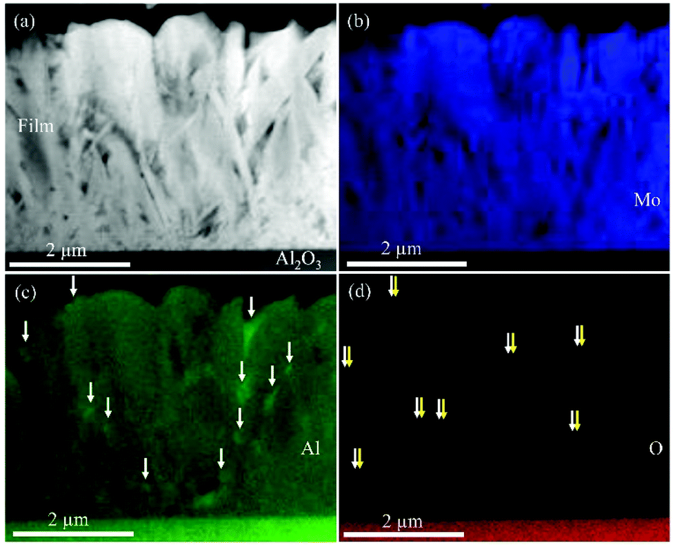 | ||
| Fig. 2 (a)–(d) Cross-sectional HAADF STEM image of the film and corresponding EDX maps of Mo, Al and O. Al- and O-rich areas are marked by white arrows in (c) and (d). Representative areas of AlOx are marked by yellow arrows in (d). | ||
In the present work, the planar film defects were studied in detail by aberration-corrected high-resolution STEM imaging (Fig. 3(a)–(d)). A HAADF STEM image is shown in Fig. 3(a) where the brightest atomic columns are Mo columns and the dark grey ones are Al, as the intensity is roughly proportional to Z2, where Z is the atomic number.33 The atomic arrangement in the ab plane is seen along the [001] viewing direction of the pristine MoAlB: Mo–Mo dumbbells of parallel orientation extend along [100] in defect-free MoAlB (marked with a yellow arrow) within the Mo2B2 subunits, which are in turn separated by two Al layers along [010]. An additional Mo layer is found in the CD type (black arrow) and in-plane zigzag Mo–Mo stacking is observed at the TB (white arrow). Al deintercalation or a local off-stochiometric composition may cause the formation of CD. The fact that TB defects form frequently within a grain is illustrated in Fig. 3(d). As seen in this figure, the TB domains can have different width. The smallest width of the TB domain is half of the lattice parameter b, which is ≈7 Å for the MoAlB, while the other one in the displayed region has a width of around ≈29 Å. The domains separate regions with different orientations. Fast Fourier transforms (FFTs) from the pristine area (zone axis [001]) and the larger TB domain (zone axis [100]) are given in Fig. 3(e) and (f). Thus, the defects are indeed 90° TB, where the individual domains extend along the [010] direction, but one is aligned along [100] and the other along [001]. More regions from different grains, showing TBs with a width from less than a nanometer to maximum 6 nm are depicted in Fig. S2 (ESI†). Such nanometer-sized domains were also reported in Cr2AlB234 but were not observed in MoAlB until now. As in Cr2AlB2, the smallest width of a TB domain is half of the lattice parameter b. In accordance with Lu et al.34 we refer to them as nanosized TB defects (Fig. 3(a)).
 | ||
| Fig. 3 (a) High magnification HAADF STEM image showing a twist grain boundary (TB) (white arrow) and a Mo3Al2B4 compositional defect (CD) (black arrow) within pristine MoAlB (yellow arrow). Here and in the following throughout the text, violet, blue and green colors represent Mo, Al, and B atomic columns, respectively. (b) Corresponding ABF STEM image comparing B positions in the TB, Mo3Al2B4 and the pristine MAB. (c) Local phase analysis depicting Mo3Al2B4 in pristine MoAlB. (d) TB boundaries separating domains with one and four units width (white bracket), respectively. The FFT of the pristine region and the three-units-wide twisted domain is shown in (e) and (f). (g, h and i) Schematic drawings of the atomistic structural models of pristine MoAlB, TB, CD, respectively. Except for TB, all structures are shown along the [001] zone axis, a and b represent the crystallographic direction. The TB separates domains with [001] and [100] orientation. | ||
As compared to HAADF STEM imaging, the intensity is proportional to Z1/3 in annular bright field images.35 Thus, it can be used for detection of the light B atoms. Fig. 3(b) depicts the in-plane atomic positions of B atoms (green dots) in the CD, as evident from ABF STEM, and compares it with the corresponding positions in the pristine structure. The CD composition is thus identified as Mo3Al2B4 by simple atom counting in the HAADF and ABF STEM images. Sample tilt36 is a well-known issue in ABF STEM imaging, hindering accurate location of light atoms inside a crystal, as picometer-level precision would require other techniques such as integrated differential phase contrast (iDPC) STEM imaging.37 Nevertheless, ABF STEM imaging can be used to assign the B position while taking a larger error into account. In addition, the B K edge transitions in STEM EELS data are considered here as proof that B is present, as discussed below.
Combined high-resolution HAADF STEM micrographs and geometrical phase analysis (GPA)38 yield quantitative maps of the local Mo–Mo interplanar spacing differences of the Mo3Al2B4-like CD, compared to the Mo–Mo interplanar spacing of pristine MoAlB (Fig. 3(c)). Herein, the map is calculated from the interplanar spacing differences, obtained by comparing the reference lattice (pristine MoAlB) – marked in the yellow square in Fig. 3(c) – with the rest of the image presented in Fig. 3(c).38 The color scale corresponds to the upper and lower limit of the total relative interplanar spacing difference; additional components of the relative interplanar spacing difference tensor (εyy) are given in the ESI (Fig. S3†). The in-plane Mo–Mo spacing map reveals a lattice spacing in Mo3Al2B4 that is up to 11% larger compared to pristine MoAlB. Interestingly, we observed MoB MBene formation in the vicinity of CD located close to the grain boundaries.24 At this stage of research it is too early to claim that Mo3Al2B4 acts as a precursor for 2D MoB synthesis, but further investigations are currently ongoing to verify this.
Schematic models of the projected atomic columns in pristine MoAlB, the TB as well as the CD are displayed in Fig. 3(g)–(i). They were used as input to construct structural models for the DFT calculations, from which the ground-state enthalpies of formation were determined. The obtained values are shown in Fig. 4. The enthalpies of formation of pristine MoAlB (Fig. 3(g)), an isolated TB in a MoAlB supercell (Fig. 3(h)) and an isolated region of a model Mo1.125AlB1.25 phase (corresponding in morphology to the CD) in a MoAlB supercell (Fig. 3(i)) are relatively close to each other, as shown in Fig. 4. This is particularly true for MoAlB and the model Mo1.125AlB1.25 phase, which was calculated using an atomic arrangement identical to that of the CD, but off-stoichiometric, due to supercell size feasibility. In addition, the energy of formation of the 2D MBene discussed in our previous study24 has also been calculated, and is lying roughly between those of the TB and CD defects.
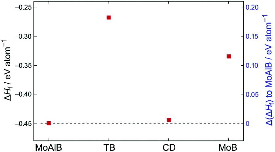 | ||
| Fig. 4 Enthalpies of formation ΔHf at the ground state (T = 0 K) from density functional theory calculations for pristine MoAlB, an isolated TB defect, an isolated analogue for the compositional defect (CD), both in a MoAlB supercell, and MoB. The left Y-axis shows the absolute values in eV per atom, the right Y-axis gives the difference to the energetically most favourable system, pristine MoAlB, indicated by the dashed line at 0 eV. | ||
It is evident from the right axis in Fig. 4 that the highest difference in ΔHf is approximately 0.18 eV per atom (for the model TB defect), whereas the minuscule enthalpic difference between the CD and the pristine phase is <0.01 eV per atom. It is well known that during magnetron sputtering,39 the magnitude of the energetic barriers predicted here can readily be overcome. Hence, the concurrent formation of all defect phases observed is expected in additon to pristine MoAlB. This assessment is based on predictions and the experimental verification of other ionically-covalently bonded sputtered thin film materials.39
Apart from the TB and CD, we frequently observed faceted grain boundaries, with a facet length of up to a few nanometers. An example is given in Fig. 5, where one grain is oriented in the [001] zone axis and the other is oriented out of the zone axis. The corresponding line profile from a HAADF STEM image (Fig. 5(a)) shows a Mo deficiency (intensity from MoI and MoII atomic columns) at the grain boundary in Fig. 5(d). Simultaneously, HAADF, ABF and ADF imaging on the same area of interest provides better visualization with respect to heavy, medium and light atoms. The stair-like atomic arrangement from Mo to B is marked at the grain boundary. The ADF STEM image in Fig. 5(b) shows that the adjacent bilayers of Al positions seem unaffected. Boron positions were analyzed with the help of ABF STEM images and we found that B planes are sandwiched between Mo, while the Al double layers are unchanged (Fig. 5(c)). The grains along [001] end with ‘stair’ structures. More examples from other grains are available in the ESI (Fig. S4†).
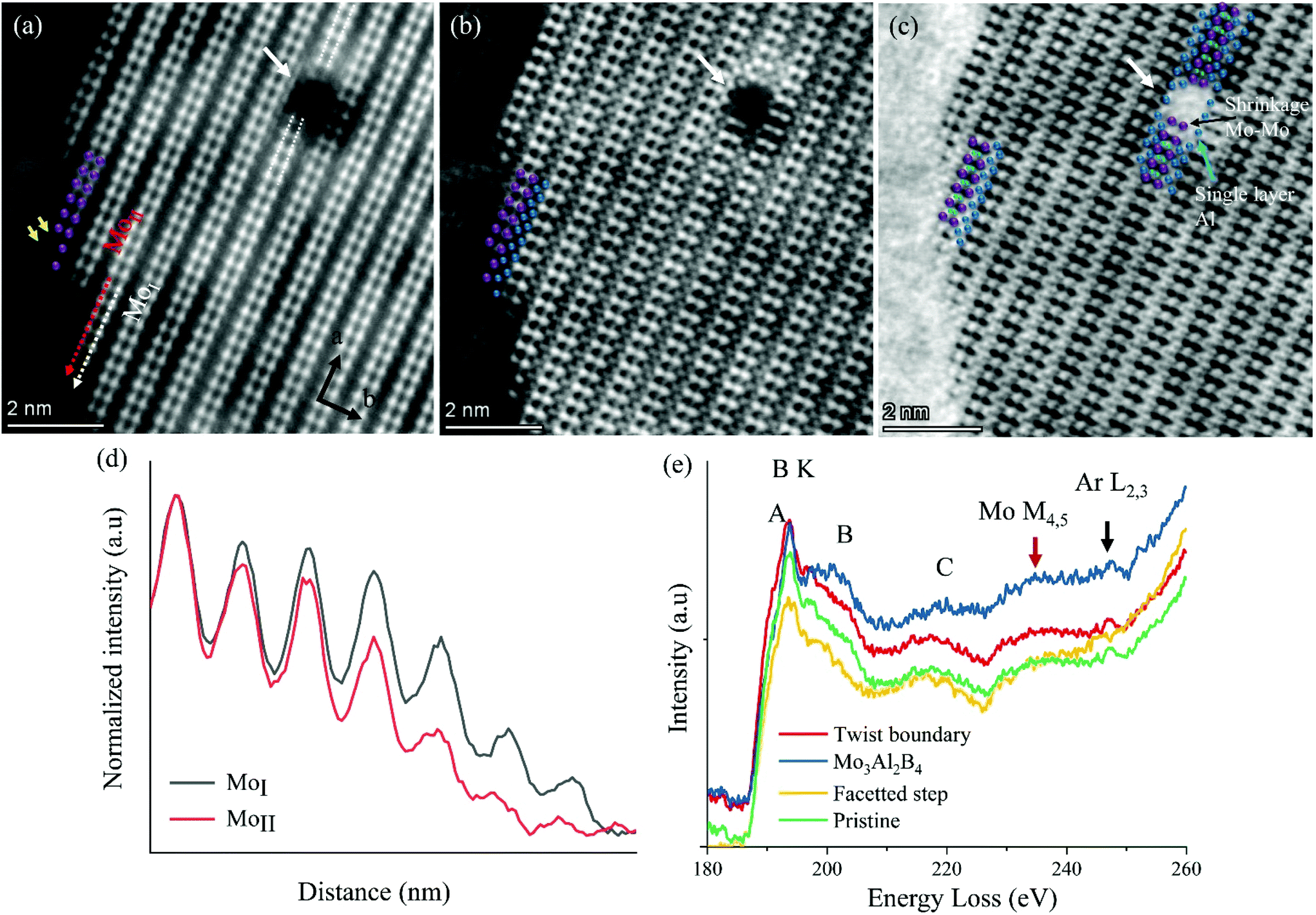 | ||
| Fig. 5 Simultaneously acquired (a) HAADF, (b) ADF and (c) ABF STEM images of a grain boundary region with one grain viewed along the [001] orientation. A 3D cluster defect is visible within the grain, marked by a white arrow. Yellow arrows indicate missing Mo atomic columns. (b) Atomic positions of both Mo and Al are marked in the ADF STEM image near the faceted region at the grain boundary. (c) B positions near the 3D cluster and at the faceted grain boundary are marked by green dots. (d) Line profile from the HAADF image, showing atomic intensity of MoI (white) and MoII (red) columns. (e) STEM EELS spectra showing B K edge, with the main peaks labelled by A, B, C. In addition, the Mo M4,5 and Ar L2,3 edges are assigned. Images (a)–(c) without color dots are available in ESI (Fig. S7†) for comparison purposes. | ||
We also observed 3D nanosized clusters in the grain interior (Fig. 5(a)–(c)). A lattice distortion in the vicinity of these clusters is clearly visible by inverse fast Fourier transformation (IFFT) (available in the ESI, Fig. S5†) and at a distance of approximately 2 nm from the cluster the distortion disappears. The atomic arrangement of each element in the vicinity of such 3D clusters is visualized by representative color dots in the ABF STEM micrograph (Fig. 5(c)). Deintercalation of Al from the double layer to a single layer is marked by a blue arrow and the shrinkage of the Mo–Mo bond by a black arrow in the ABF STEM image. At this point, the interplanar Mo–Mo distance (white dotted line in Fig. 5(a)) is shortened by 5–6% compared to the pristine MoAlB region. A HAADF STEM image and corresponding line profile, showing the presence of an Al single layer in the vicinity of a 3D cluster, are available in the ESI (Fig. S6†). Similar 3D cluster defects were observed in a Mo2BC/Cr2AlC coating.40,41 They might be caused by the bombardment with ions of the starting materials and Ar ions in the DC magnetron sputtering chamber.
EELS studies were carried out on these various structural defects to compare changes in their fine features with the pristine MoAlB area in Fig. 5(e). In the depicted energy loss regime in Fig. 5(e), the element-specific edges of B K (peak A, B, C) and Mo M4,5 (marked by the red arrow) are present. The energy-loss near-edge structure (ELNES) of the B K edge illustrates transitions from 1s to unoccupied π* states (sharp peak A) and σ* states (peak B) while peak C can be an effect of plasmon contributions.42,43 The onset of the B K edge is roughly identical for all defects, starting from 186.8 eV. A minute splitting of peak A was noticed at the faceted grain boundary structure. It is also well known in literature that the B K edge is coordination-sensitive,44 so closer investigation of the changes of peak B and C here is warranted. The observed changes in the fine structure of peaks B and C distinguish local electronic states of the structural defect from those of the pristine layer. As an example, the broader C peak seems to be flattened in Mo3Al2B4. Similar comparative spectral changes in the Mo M4,5 bump (red arrow, around 234 eV) are observed in this plot. Besides that, the film absorbed Ar, as evidenced by the presence of the Ar L2,3 edge around approx. 247 eV, signified by the black arrow. These minute changes in the fine structural features demonstrate the strength of EELS as a nanoscale electronic structure measurement method, where no alternative technique exists in terms of simultaneous imaging and spectroscopy at atomic length scale.
5. Conclusions
In summary, we demonstrate that various previously unreported structural defects forming in an orthorhombic MoAlB matrix at moderate temperature were identified by advanced STEM imaging. A 90° twist boundary along with a newly formed compositional defect (Mo3Al2B4) were observed. Correlating aberration-corrected HR(S)TEM with GPA provides a maximum 11% larger lattice plane of a newly formed Mo3Al2B4 MAB phase compared to pristine MoAlB. Formation enthalpy differences from DFT between the defect phases and the pristine MoAlB phase are minute and thus readily overcome during sputtering. Hence, the concurrent phase formation of TB, CD and MoB, observed by a combination of advanced imaging techniques, is consistent with ab initio predictions. Apart from 2D twist boundaries and 3D compositional defects, 3D amorphous clusters were observed. Overall, the analysis demonstrated how the correlation between advanced imaging techniques such as HAADF, ADF and ABF STEM allowed us to identify the above mentioned defect phases. The nature of these structural defects may have a strong impact on the feasibility of Al deintercalation and formation of 2D MoB MBene.Author contributions
R. S., D. B., J. M. S. and C. S. conceived the research. R. S. performed the advanced STEM work with support from C. S. The manuscript was drafted by R. S. with support from D. B., J. M. S. and C. S. D. B. performed and interpreted the DFT calculations and J.-O. A. synthesized the thin film. All authors then contributed and have given approval to the final version of the manuscript.Conflicts of interest
The authors declare no competing financial interests.Acknowledgements
D. B. and J. M. S. thank the IT Center of RWTH Aachen University for the provision of computational resources and IT support via the Jülich-Aachen Research Alliance's (JARA) JARA0206 grant. J. M. S. acknowledges financial support from the MPG fellow program. Open Access funding provided by the Max Planck Society.References
- W. Rieger, H. Nowotny and F. Benesovsky, Über einige Komplexboride von Übergangsmetallen, Monatsh. Chem. Verw. Teile Anderer Wiss., 1965, 96, 844–851 CrossRef.
- S. Kota, M. Sokol and M. W. Barsoum, A progress report on the MAB phases: atomically laminated, ternary transition metal borides, Int. Mater. Rev., 2020, 65(4), 226–255 CrossRef CAS.
- M. Khazaei, J. Wang, M. Estili, A. Ranjbar, S. Suehara, M. Arai, K. Keivan Esfarjani and S. Yunoki, Novel MAB phases and insights into their exfoliation into 2D MBenes, Nanoscale, 2019, 11, 11305–11314 RSC.
- N. F. Rosli, M. Z. M. Nasir, N. Antonatos, Z. Sofer, A. Dash, J. Gonzalez-Julian, A. C. Fisher, R. D. Webster and M. Pumera, MAX and MAB Phases: Two-Dimensional Layered Carbide and Boride Nanomaterials for Electrochemical Applications, ACS Appl. Nano Mater., 2019, 2(9), 6010–6021 CrossRef CAS.
- Z. Sun, D. Music, R. Ahuja, S. Li and J. M. Schneider, Bonding and classification of nanolayered ternary carbides, Phys. Rev. B: Condens. Matter Mater. Phys., 2004, 70, 092102 CrossRef.
- F. Li, S. Sun, Y. Xu, L. Tian, Y. Wang, Z. Xu and R. Li, Microstructure and Wear Behaviors of Plasma-Sprayed MoAlB Ceramic Coating, Coatings, 2021, 11, 474 CrossRef CAS.
- J.-O. Achenbach, R. Sahu, B. Völker, M. Hans, D. Primetzhofer, D. J. Miljanovic, C. Scheu and J. M. Schneider, Synthesis and Properties of Orthorhombic MoAlB Coatings, Coatings, 2019, 9(8), 510 CrossRef CAS.
- L. T. Alameda, C. F. Holder, J. L. Fenton and R. E. Schaak, Partial etching of Al from MoAlB single crystal to expose catalytically active basal planes for the hydrogen evolution reaction, Chem. Mater., 2017, 29, 8953–8957 CrossRef CAS.
- Y. Fu, P. Richardson, K. Li, H. Yu, B. Yu, S. Donne, E. Kisi and T. Ma, Transition Metal Aluminum Boride as a New Candidate for Ambient-Condition Electrochemical Ammonia Synthesis, Nano-Micro Lett., 2020, 12(1), 1–13 CrossRef PubMed.
- Z. Guo, J. Zhou and Z. Sun, New two-dimensional transition metal borides for Li ion batteries and electrocatalysis, J. Mater. Chem. A, 2017, 5, 23530–23535 RSC.
- T. Zhang, B. Zhang, Q. Peng, J. Zhou and Z. Sun, Mo2B2 MBene-supported single-atom catalysts as bifunctional HER/OER and OER/ORR electrocatalysts, J. Mater. Chem. A, 2021, 9, 433–441 RSC.
- L. Xu, O. Shi, C. Liu, D. Zhu, S. Grasso and C. Hu, Synthesis, microstructure and properties of MoAlB ceramics, Ceram. Int., 2018, 44, 13396–11340 CrossRef CAS.
- X. Lu, S. Li, W. Zhang, B. Yao, W. Yu and Y. Zhou, Crack healing behavior of a MAB phase: MoAlB, J. Eur. Ceram. Soc., 2019, 39, 4023–4028 CrossRef CAS.
- S. Kota, E. Zapata-Solvas, A. Ly, J. Lu, O. Elkassabany, A. Huon, W. E. Lee, L. Hultman, S. J. May and M. W. Barsoum, Synthesis and characterization of an alumina forming nanolaminated boride: MoAlB, Sci. Rep., 2016, 6, 26475 CrossRef CAS PubMed.
- L. T. Alameda, P. Moradifar, Z. P. Metzger, N. Alem and R. E. Schaak, Topochemical deintercalation of Al from MoAlB: stepwise etching pathway, layered intergrowth structures, and two-dimensional MBene, J. Am. Chem. Soc., 2018, 140(28), 8833–8840 CrossRef CAS PubMed.
- L. T. Alameda, R. W. Lord, J. A. Barr, P. Moradifar, Z. P. Metzger, B. C. Steimle, C. F. Holder, N. Alem, S. B. Sinnott and R. E. Schaak, Multi-Step Topochemical Pathway to Metastable Mo2AlB2 and Related Two-Dimensional Nanosheet Heterostructures, J. Am. Chem. Soc., 2019, 141(27), 10852–10861 CrossRef CAS PubMed.
- S. Evertz, P. Pöllmann, D. M. Holzapfel, E. Mayer and J. M. Schneider, Low temperature synthesis of dense MoAlB thin films, J. Eur. Ceram. Soc., 2021, 41(13), 6302–6308 CrossRef CAS.
- S. K. Aghda, D. Music, Y. Unutulmazsoy, H. H. Sua, S. Mráz, M. Hans, D. Primetzhofer, A. Anders and J. M. Schneider, Unravelling the ion-energy-dependent structure evolution and its implications for the elastic properties of (V, Al) N thin films, Acta Mater., 2021, 214, 117003 CrossRef.
- D. M. Holzapfel, D. Music, M. Hans, S. Wolff-Goodrich, D. Holec, D. Bogdanovski, M. Arndt, A. O. Eriksson, K. Yalamanchili, D. Primetzhofer, C. H. Liebscher and J. M. Schneider, Enhanced thermal stability of (Ti,Al)N coatings by oxygen incorporation, Acta Mater., 2021, 218, 117204 CrossRef CAS.
- A. Saksena, Y. C. Chien, K. Chang, P. Kümmerl, M. Hans, B. Völker and J. M. Schneider, Metastable phase formation of Pt-X (X = Ir, Au) thin films, Sci. Rep., 2018, 8, 10198 CrossRef PubMed.
- T. Unold, I. Sieber and K. Ellmer, Efficient CuInS2 solar cells by reactive magnetron sputtering, Appl. Phys. Lett., 2006, 88, 213502 CrossRef.
- S. Gleich, H. Fager, H. Bolvardi, J.-O. Achenbach, R. Soler, K. G. Pradeep, J. M. Schneider, G. Dehm and C. Scheu, Nanostructure of and structural defects in a Mo2BC hard coating investigated by transmission electron microscopy and atom probe tomography, J. Appl. Phys., 2017, 122(7), 075305 CrossRef.
- A. Jamnig, N. Pliatsikas, M. Konpan, J. Lu, T. Kehagias, A. N. Kotanidis, N. Kalfagiannis, D. V. Bellas, E. Lidorikis, J. Kovac, G. Abadias, I. Petrov, J. E. Greene and K. Sarakinos, 3D-to-2D Morphology Manipulation of Sputter-Deposited Nanoscale Silver Films on Weakly Interacting Substrates via Selective Nitrogen Deployment for Multifunctional Metal Contacts, ACS Appl. Nano Mater., 2020, 3(5), 4728–4738 CrossRef CAS.
- R. Sahu, D. Bogdanovski, J.-O. Achenbach, S. Zhang, M. Hans, D. Primetzhofer, J. M. Schneider and C. Scheu, Direct MoB MBene domain formation in magnetron sputtered MoAlB thin films, Nanoscale, 2021, 13, 18077–18083 RSC.
- G. Kresse and J. Hafner, Ab initio molecular dynamics for liquid metals, Phys. Rev. B: Condens. Matter Mater. Phys., 1993, 47(1), 558–561 CrossRef CAS PubMed.
- G. Kresse and J. Furthmüller, Efficiency of ab initio total energy calculations for metals and semiconductors using a plane-wave basis set, Comput. Mater. Sci., 1996, 6(1), 15–50 CrossRef CAS.
- G. Kresse and D. Joubert, From ultrasoft pseudopotentials to the projector augmented-wave method, Phys. Rev. B: Condens. Matter Mater. Phys., 1999, 59(3), 1758–1775 CrossRef CAS.
- P. E. Blöchl, Projector augmented-wave method, Phys. Rev. B: Condens. Matter Mater. Phys., 1994, 50(24), 17953–17979 CrossRef PubMed.
- J. P. Perdew, K. Burke and M. Ernzerhof, Generalized Gradient Approximation Made Simple, Phys. Rev. Lett., 1996, 77(18), 3865–3868 CrossRef CAS PubMed.
- H. J. Monkhorst and J. D. Pack, Special points for Brillouin-zone integrations, Phys. Rev. B: Condens. Matter Mater. Phys., 1976, 13(12), 5188–5192 CrossRef.
- M. Ade and H. Hillebrecht, Ternary Borides Cr2AlB2, Cr3AlB4, and Cr4AlB6: The First Members of the Series (CrB2)nCrAl with n = 1, 2, 3 and a Unifying Concept for Ternary Borides as MAB-Phases, Inorg. Chem., 2015, 54(13), 6122–6135 CrossRef CAS PubMed.
- J. M. Schneider, K. Larsson, J. Lu, E. Olsson and B. Hjörvarsson, Role of hydrogen for the elastic properties of alumina thin films, Appl. Phys. Lett., 2002, 80, 1144–1146 CrossRef CAS.
- S. J. Pennycook and P. D. Nellist, Scanning transmission electron microscopy, Springer, New York, 2011 Search PubMed.
- J. Lu, S. Kota, S. M. W. Barsoum and L. Hultman, Atomic structure and lattice defects in nanolaminated ternary transition metal boride, Mater. Res. Lett., 2017, 5(4), 235–241 CrossRef CAS.
- S. D. Findlay, N. Shibata, H. Sawada, E. Okunishi, Y. Kondo and Y. Ikuhara, Dynamics of annular bright field imaging in scanning transmission electron microscopy, Ultramicroscopy, 2010, 110(7), 903–923 CrossRef CAS PubMed.
- D. Zhou, K. Müller-Caspary, W. Sigle, F. F. Krause, A. Rosenauer and P. A. van Aken, Sample tilt effects on atom column position determination in ABF–STEM imaging, Ultramicroscopy, 2017, 160, 110–117 CrossRef PubMed.
- I. Lazić, E. G. T. Bosch and S. Lazar, Phase contrast STEM for thin samples: Integrated differential phase contrast, Ultramicroscopy, 2016, 160, 265 CrossRef PubMed.
- M. J. Hÿtch, E. Snoeck and R. Kilaas, Quantitative measurement of displacement and strain fields from HREM micrographs, Ultramicroscopy, 1998, 74, 131–146 CrossRef.
- P. H. Mayrhofer, D. Music and J. M. Schneider, Influence of the Al distribution on the structure, elastic properties, and phase stability of supersaturated Ti1−xAlxN, J. Appl. Phys., 2006, 100, 094906 CrossRef.
- S. Gleich, R. Soler, H. Fager, H. Bolvardi, J.-O. Achenbach, M. Hans, D. Primetzhofer, J. M. Schneider, G. Dehm and C. Scheu, Modifying the nanostructure and the mechanical properties of Mo2BC hard coatings: Influence of substrate temperature during magnetron sputtering, Mater. Des., 2018, 142, 203–211 CrossRef CAS.
- Y. T. Chen, D. Music, L. Shang, J. Mayer and J. M. Schneider, Nanometre-scale 3D defects in Cr2AlC thin films, Sci. Rep., 2017, 7, 984 CrossRef CAS PubMed.
- F. Fossard, L. Sponza, L. Schué, C. Attaccalite, F. Ducastelle, J. Barjon and A. Loiseau, Angular resolved electron energy loss spectroscopy in hexagonal boron nitride, Phys. Rev. B: Condens. Matter Mater. Phys., 2017, 96, 115304 CrossRef.
- K. N. Kushita, K. Hojou and S. Furuno, In Situ EELS and TEM Observation of Boron Carbide (B4C) During Hydrogen- and Helium-Ion Bombardments, Microsc., Microanal., Microstruct., 1995, 6, 149–157 CrossRef CAS.
- L. A. J. Garvie, A. J. Craven and R. Brydson, Parallel electron energy-loss spectroscopy (PEELS) study of B in minerals: The electron energy-loss near-edge structure (ELNES) of the B K edge, Am. Mineral., 1995, 80, 1132–1144 CAS.
Footnote |
| † Electronic supplementary information (ESI) available. See DOI: 10.1039/d1nr07792a |
| This journal is © The Royal Society of Chemistry 2022 |