Metallic vs. semiconducting properties of quasi-one-dimensional tantalum selenide van der Waals nanoribbons†
Abstract
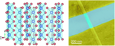
We conducted a tip-enhanced Raman scattering spectroscopy (TERS) and photoluminescence (PL) study of quasi-1D TaSe3−δ nanoribbons exfoliated onto gold substrates. At a selenium deficiency of δ ∼ 0.25 (Se/Ta = 2.75), the nanoribbons exhibit a strong, broad PL peak centered around ∼920 nm (1.35 eV), suggesting their semiconducting behavior. Such nanoribbons revealed a strong TERS response under 785 nm (1.58 eV) laser excitation, allowing for their nanoscale spectroscopic imaging. Nanoribbons with a smaller selenium deficiency (Se/Ta = 2.85, δ ∼ 0.15) did not show any PL or TERS response. The confocal Raman spectra of these samples agree with the previously-reported spectra of metallic TaSe3. The differences in the optical response of the nanoribbons examined in this study suggest that even small variations in Se content can induce changes in electronic band structure, causing samples to exhibit either metallic or semiconducting character. The temperature-dependent electrical measurements of devices fabricated with both types of materials corroborate these observations. The density-functional-theory calculations revealed that substitution of an oxygen atom in a Se vacancy can result in band gap opening and thus enable the transition from a metal to a semiconductor. However, the predicted band gap is substantially smaller than that derived from the PL data. These results indicate that the properties of van der Waals materials can vary significantly depending on stoichiometry, defect types and concentration, and possibly environmental and substrate effects. In view of this finding, local probing of nanoribbon properties with TERS becomes essential to understanding such low-dimensional systems.


 Please wait while we load your content...