DOI:
10.1039/D1NR07746E
(Paper)
Nanoscale, 2022,
14, 2722-2728
A voltage-controllable VO2 based metamaterial perfect absorber for CO2 gas sensing application
Received
24th November 2021
, Accepted 12th January 2022
First published on 12th January 2022
Abstract
Vanadium dioxide (VO2) based metamaterial perfect absorbers (MPAs) have high potential application values in sensing gas molecules. However, a tuning mechanism via temperature manipulation lacks the compatibility with electronic devices. In this study, a voltage-controllable device is proposed by integrating an MPA and micro-electro-mechanical system (MEMS) based microheater for CO2 gas sensing application. The MPA is composed of a metal–dielectric–metal (MDM) structure and tailored to form an H-shaped metamaterial. The central bar of the H-shaped metamaterial is composed of a VO2 material, which exhibits perfect absorption in the CO2 gas absorption spectrum, i.e., at a wavelength of 2.70 μm. The intergated microheater is patterned by using fractal theory to provide high heating temperature and high uniformity of surface temperature. By precisely driving a DC bias voltage on the microheater, the MPA is heated and it can exhibit switchable optical properties with high efficiency. These results provide a strategy to open an avenue for sensors, absorbers, switches, and programmable devices in infrared wavelength range applications.
1. Introduction
Recently, metamaterial absorbers have shown good prospects due to their ability to control the propagation of electromagnetic (EM) waves.1–4 They provide the opportunities to realize unique EM properties for widespread applications, such as invisibility cloaks, perfect absorbers, super lenses, and solar cells.5–10 Metamaterial perfect absorbers (MPAs) have been proposed to realize nearly 100% absorption in the wide EM spectrum from microwave,11 and terahertz (THz)12 to infrared (IR)13–15 wavelength ranges. Since many surrounding gas molecules exhibit identical vibration frequency to IR light, they can be distinguished in the IR wavelength range. The development of an MPA-based IR gas sensor has become a research hotspot owing to its high selectivity and high robustness.16 Many MPA-based sensors have been demonstrated with powerful performances.17–19 However, they cannot be actively tuned once fabricated while the tunable characteristic is desired in real applications by using an external stimulus. Micro-electro-mechanical system (MEMS) technology is one of the most important tuning mechanisms to control the MPA.20 By directly adjusting the geometrical dimensions of the metamaterial unit cell, the MEMS-based metamaterial exhibits a large tuning range and good linearity in sensing applications.21–24
Furthermore, vanadium dioxide (VO2) based metamaterials are widely studied for their active tunability via temperature manipulation.25 VO2 is a well-known material while the insulator-to-metal transition characteristic can be induced thermally, optically or electrically at the time scale of picoseconds due to the atomic level deformation for sensing applications or active phase change material-based control.26–32 By improving the internal temperature above the critical temperature, dramatic changes of electrical conductivity can be realized in VO2. They are reflected in the optical dielectric properties of VO2 to control the propagation of EM waves with high efficiency. Due to the ultrafast switching time of VO2, it is demonstrated to be integrated with metamaterial for numerous practical applications, such as modulators, programmable devices, and tunable antennas.33–36
In this work, a CO2 gas sensor is proposed by integrating an H-shaped MPA and MEMS-based microheater to form a voltage-controllable device. The microheater is patterned using mathematical fractal theory and named the Peano-shaped microheater. The thermal emission of the Peano-shaped microheater can fully cover the heating area uniformly. There are many literature reported VO2 based metamaterials to investigate their tunable EM properties by changing heating temperature.37 While such a thermal tuning method lacks the compatibility with electronic devices, an integrated MEMS-based microheater is desired to provide a precise voltage-controllable characteristic. The Peano-shaped microheater can collect all flowing electric energy and then convert it into thermal energy. By increasing the heating temperature of the Peano-shaped microheater, the surface temperature is distributed uniformly compared with that of a traditional winding-shaped microheater. The MEMS-based MPA can exhibit perfect absorption with precisely controlled voltage at a wavelength of 2.70 μm, which is the CO2 absorption spectrum. It is suitable to be used as a CO2 gas sensor with high sensitivity. Moreover, such perfect absorption can be continuously switched to be applied in many fields, such as IR switches, programmable IR devices, and IR detectors.
2. Designs and methods
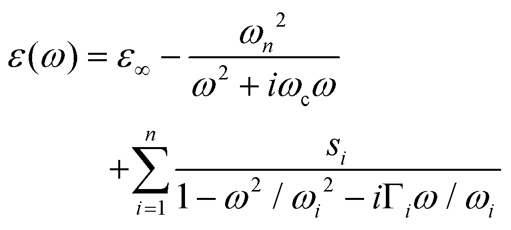
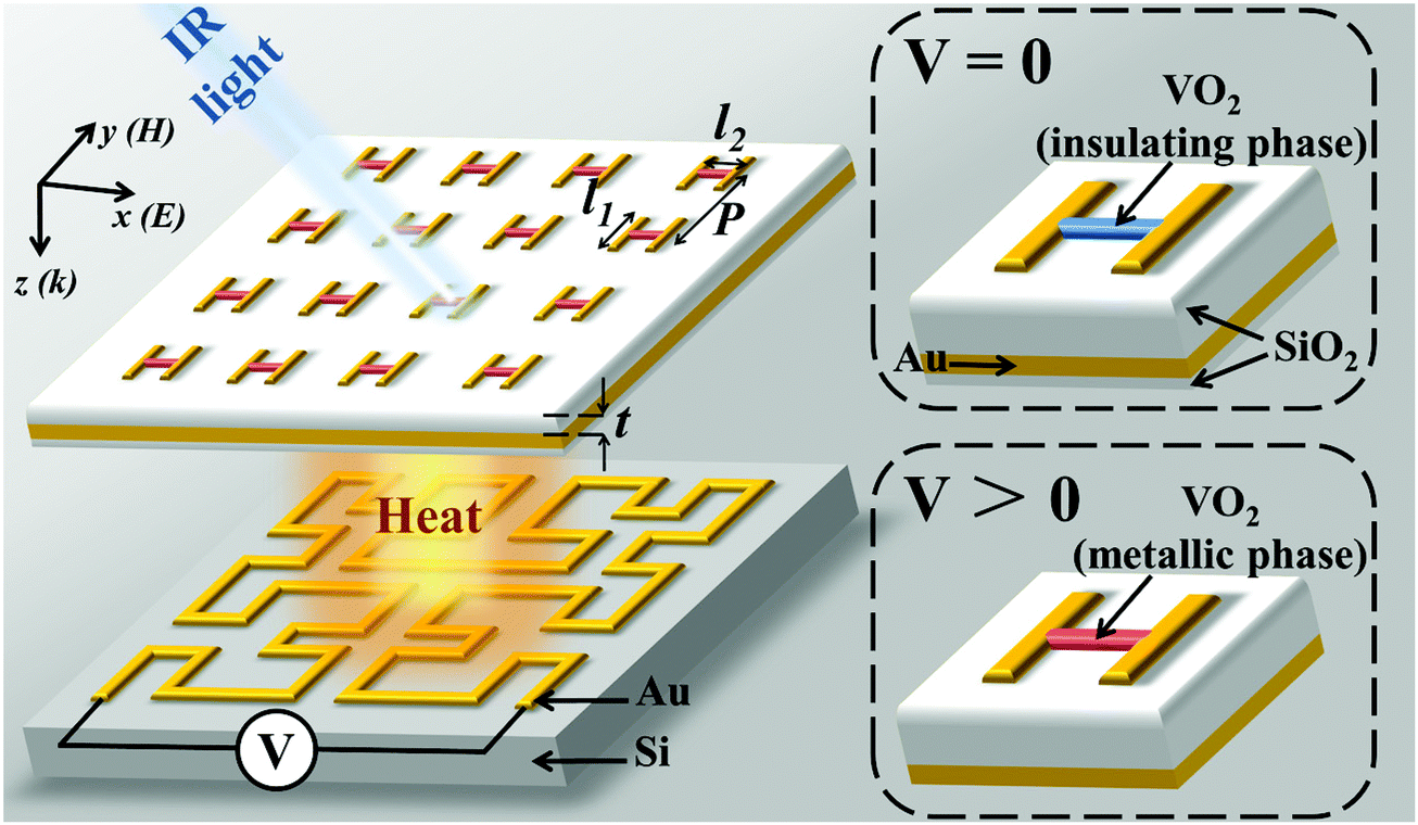
Fig. 1 illustrates the 3D schematic drawing and tuning mechanism of MEMS-based MPA design. Such a design is composed of an H-shaped MPA on the top and a Peano-shaped microheater on the bottom. The compositions of the H-shaped MPA are Au/VO2 on SiO2 and Au from top to bottom. The top Au and VO2 thin-films are 300 nm in thickness, and are tailored to form an H-shaped periodic array. The middle transverse bar is patterned by using the VO2 material to provide active tunability as shown in the inserted image of Fig. 1. Meanwhile, the key parameters of the H-shaped MPA unit cell are also denoted in Fig. 1, including the thickness of the dielectric layer (t), and lengths of the longitudinal bar (l1), and transverse bar (l2). The period (P) of the H-shaped MPA unit-cell is kept constant at 2.3 μm. For the Peano-shaped microheater, an Au thin-film is deposited and patterned by using mathematical fractal theory on the Si substrate. The high resistance heat is generated by the flowing electric current in the metallic loop. Such a Peano-shaped microheater provides high heating temperature and high uniformity of surface temperature. The heating area is 200 × 200 μm2. The dielectric layer between the top H-shaped MPA and the bottom Peano-shaped microheater is composed of SiO2 material, whose thickness is 5 nm to perform electrical insulating and thermal conducting functions. By driving a direct current (DC) bias voltage to the electrodes of the microheater, some heat is generated and it flows to the top metamaterial pattern, which can improve the internal temperature of the metamaterial with high efficiency. At room temperature, the VO2 thin-film is operated in the insulating state. By increasing the heating temperature higher than the phase transition temperature, the structural transformation is induced and the VO2 bar of the MPA turns into a metallic phase. The complex dielectric properties of the VO2 thin-film in both metallic and insulating phases can be described by a classical Drude–Lorentz model, which is expressed by38| | 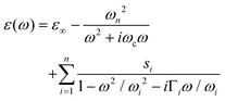 | (1) |
where ε∞ is a constant contribution to the real part of the dielectric constant from high-frequency electronic transition, ωn is the carrier density parameter, ωc is the collision frequency, si is the strength, and Γi is the linewidth. In the third term of eqn (1), the strength si, resonant frequency ωi and scattering rate Γi/ωi are temperature dependent parameters due to the interband transitions of bound electrons effected by temperature. The EM characteristics of the proposed H-shaped MPA are achieved through Lumerical solution's finite difference time domain-based simulations. The perfectly matched layer boundary conditions are assumed in the z-axis direction to evaluate the absorptivity, while the periodic boundary conditions are adopted in both the x- and y-axis directions to calculate the coupling effect between the neighboring meta-atoms.
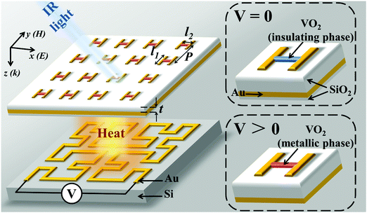 |
| | Fig. 1 Schematic drawing and tuning mechanism of MEMS-based MPA design. The periods of unit cells are kept as P = 2.3 μm. | |
3. Results and discussion
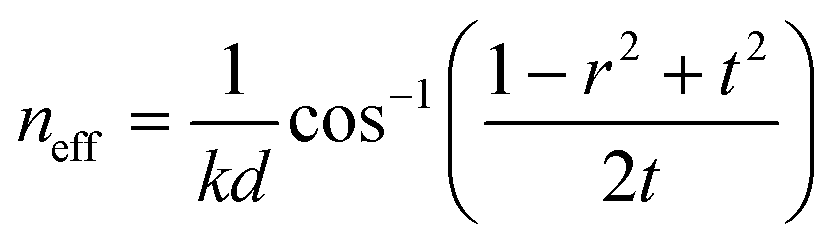
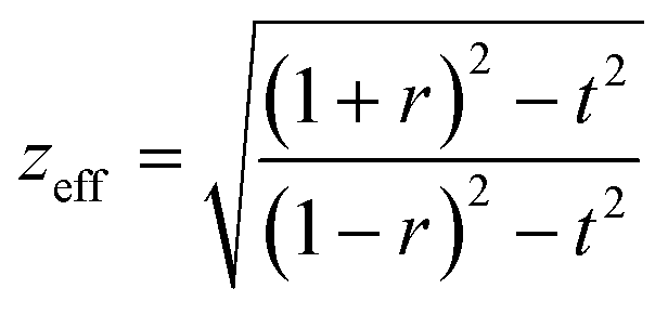
The propagation of EM waves in the H-shaped MPA is controllable by appropriately manipulating the geometric dimensions. According to the effective medium approximation, the effective refraction index and impedance index of metamaterials are calculated by39| | 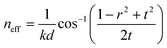 | (2) |
| |  | (3) |
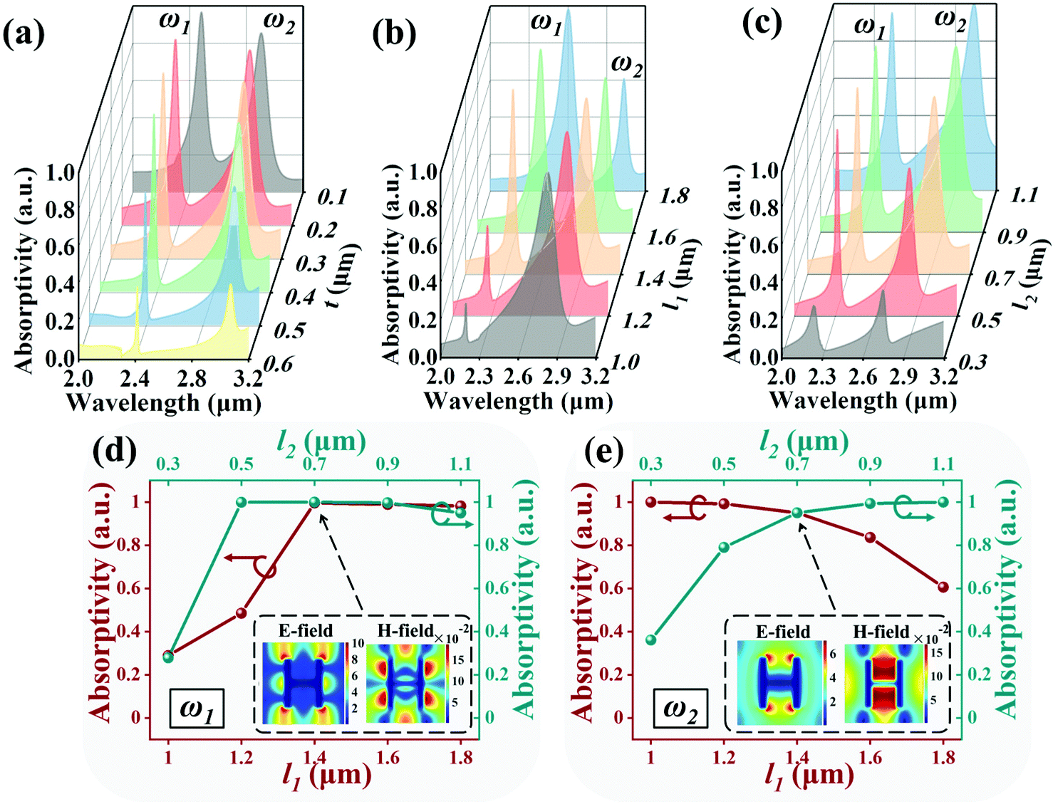
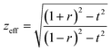
where εeff and μeff are the effective permittivity and permeability of the metamaterial, respectively, r is the reflection coefficient, t is the transmission coefficient, k is the incident wave vector, and d is the metamaterial thickness. By appropriately designing the dielectric properties of VO2, the effective impedance of the H-shaped MPA can be matched with that of the free space and then achieve zero reflection and perfect absorption. Three key parameters of the H-shaped MPA are investigated to optimize the optical properties, including t, l1 and l2 values. Herein, they are individually adjusted while the other two parameters are kept constant. Meanwhile, the VO2 bar is assumed to be phase transited in the metallic state. In the absorption spectra of Fig. 2, it can be clearly observed that such designs exhibit a dual-band characteristic in the IR wavelength range from 2.00 μm to 3.20 μm. The resonance operated at a short wavelength is denoted as ω1 while the resonance operated at a long wavelength is denoted as ω2. The t parameter determines the absorption intensity by affecting the coupling efficiency between the H-shaped metamaterial and the bottom Au mirror layers as shown in Fig. 2(a). By increasing the t value from 0.1 μm to 0.6 μm, the ω1 resonance of the H-shaped MPA is blue-shifted from the wavelength of 2.49 μm to 2.41 μm, while the absorptivity is enhanced and then decays from 0.97 to 0.39. Similarly, the ω2 resonance is red-shifted from the wavelength of 2.91 μm to 3.07 μm, while the absorptivity is enhanced and then decays from 0.85 to 0.40. When the t value is 0.3 μm, the ω1 resonance achieves perfect absorption. Therefore, the condition of 0.3 μm is suitable for the design of the H-shaped MPA with perfect IR absorption application. In Fig. 2(b and c), the variations of l1 and l2 values also affect the coupling efficiency of the H-shaped MPA by controlling the dual-resonance in the x–y plane. By increasing the l1 value, the ω1 resonance of the H-shaped MPA is red-shifted from the wavelength of 2.20 μm to 2.61 μm, while the ω2 resonance is red-shifted from the wavelength of 2.83 μm to 3.04 μm. Herein, the absorptivity is essential in the sensing application and the relationships of absorptivity of the H-shaped MPA with different l1 and l2 values at ω1 and ω2 resonances are summarized in Fig. 2(d) and (e), respectively. By increasing the l1 value from 1.0 μm to 1.8 μm, the absorptivity of the ω1 resonance is enhanced from 0.29 to 0.98 and that of the ω2 resonance decays from 0.99 to 0.61. In addition, the l2 parameter also determines the EM properties of the H-shaped MPA. By increasing the l2 value from 0.3 μm to 1.1 μm, the ω1 resonance is red-shifted from the wavelength of 2.24 μm to 2.43 μm and the ω2 resonance is red-shifted from the wavelength of 2.75 μm to 3.05 μm. The absorptivity of the ω1 resonance is enhanced from 0.28 to 0.95 and that of the ω2 resonance is enhanced from 0.36 to 0.99. Such strong resonances can be explained by the corresponding E- and H-field distributions as shown in the inset images of Fig. 2(d) and (e), which show strong E-field energies around the periodic unit cells of the H-shaped MPA. In view of the above results, the optimized parameters of the H-shaped MPA are t = 0.3 μm, l1 = 2.0 μm, and l2 = 0.7 μm to achieve perfect absorption at a wavelength of 2.70 μm for CO2 sensing application. Furthermore, the absorptivity of the H-shaped MPA can be tuned by changing the geometric dimensions for IR variable optical attenuator (VOA) application.
 |
| | Fig. 2 Absorptivity of the H-shaped MPA with different (a) t, (b) l1, and (c) l2 values, respectively. The relationships of the resonance intensities of the H-shaped MPA with different l1 and l2 values at (d) ω1 and (e) ω2 resonances, respectively. The inserted images show the corresponding E-field and H-field distributions under the conditions of l1 = 1.4 μm and l2 = 0.7 μm. | |
Since the meta-atom of the H-shaped MPA shows an anisotropic pattern, the EM properties can be controlled by incident polarization light. The absorption spectra operated at different polarization angles (θ) are illustrated in Fig. 3(a). To clearly evaluate the polarization-dependent characteristic of MPA, θ is defined as the included angle of the E-field and x-axis direction. Herein, θ equals 0° is regarded as the transverse electric (TE) mode and 90° is regarded as the transverse magnetic (TM) mode. It is clearly observed that the dual-band characteristic of the H-shaped MPA is gradually tuned to a single-band characteristic by changing the θ value from 0° to 90°. It can serve as a polarizer in the IR wavelength range. Under the condition of θ = 90°, the H-shaped MPA exhibits the maximum absorptivity of 0.44 at a wavelength of 2.40 μm. The corresponding E- and H-field distributions are shown in Fig. 3(b). The H-field distributions in the TM mode at a wavelength of 2.40 μm are much weaker than those in the TE mode at a wavelength of 2.70 μm. It explains the lower absorption which is caused by the TM mode. These polarization-dependent characteristics of the H-shaped MPA can be potentially used in IR polarization switching, VOA, and sensing applications.
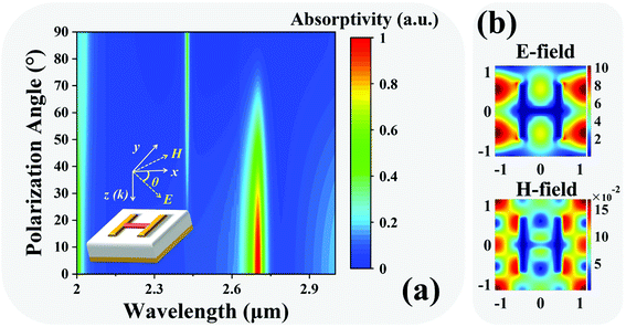 |
| | Fig. 3 (a) Absorptivity of the H-shaped MPA at different polarization angles. (b) The corresponding E-field and H-field distributions with a polarization angle of 90° at a wavelength of 2.40 μm. | |
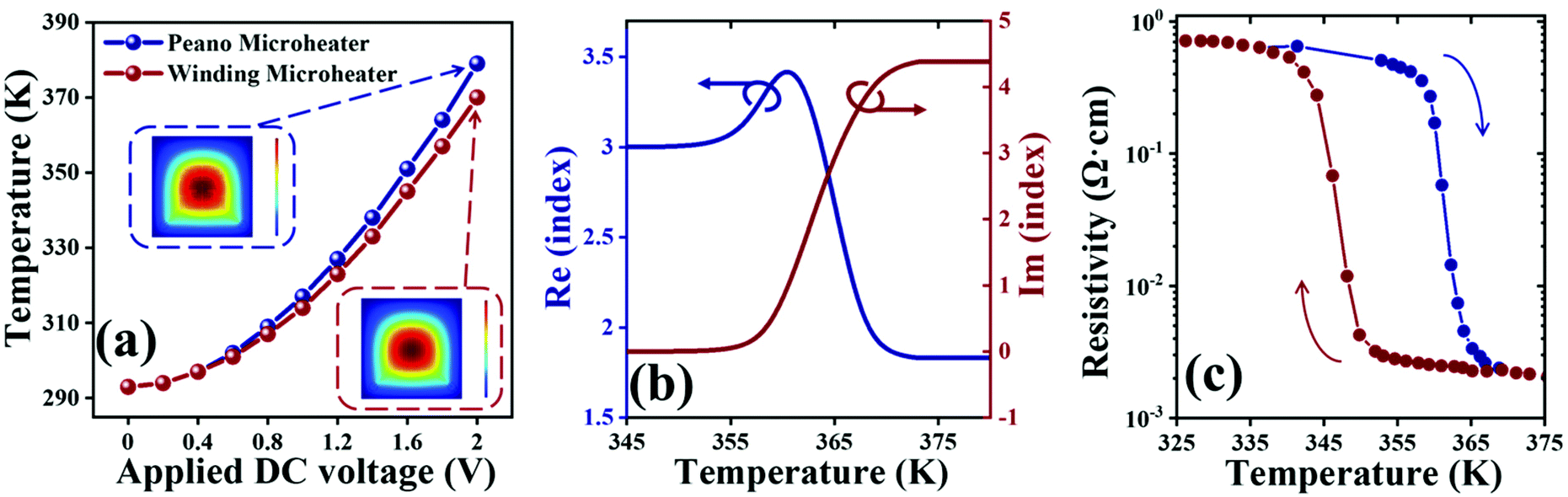
To endow the H-shaped MPA with active tunability, the Peano-shaped microheater is integrated to control the internal temperature of the H-shaped MPA with high efficiency. This voltage-controllable metamaterial design is desired to realize large-scope applications and it is worth investigating the electrical and thermal properties of the device. The relationships between the applied DC voltages and heating temperatures for the Peano-shaped microheater and the conventional winding-shaped microheater are illustrated in Fig. 4(a). The material of the microheater is adopted as the Au material with a thermal conductivity of 317 W (m K)−1. By driving a DC bias voltage on the electrodes of microheaters, the resistance heat can be generated and conducted to the H-shaped MPA to improve the surface temperature. In real applications, the top metamaterial layer is designed on the central area of the microheater while the area of the metamaterial is much smaller than that of the microheater. Therefore, the heating temperature is adopted as the maximum surface temperature. Moreover, the thickness of the SiO2 layer between the microheater and MPA is 5 nm to perform the excellent thermal conducting function. In such a design, the thermal energy is highly efficiently and highly uniformly propagated to the metamaterial layer. It can be clearly observed that the Peano-shaped microheater shows a higher temperature of 379 K and the winding-shaped microheater is 370 K at a driving voltage of 2.0 volts. It means that the Peano-shaped microheater exhibits less thermal dissipation with identical electrical power and then the energy consumptions can be further reduced. The heating power is concentrated in the central area of the microheaters. The effective heating area covers over 75% and exhibits the maximum temperature over 90%. It endows the H-shaped MPA with high-robust EM properties. Thus, the insulator-to-metal transition of VO2 can be induced thermally, which will increase the conductivity of VO2 and reduce the optical transmission in the near-IR wavelength range. These results reflect the variation of optical dielectric properties. Fig. 4(b) shows the relationship between the index of VO2 and heating temperature. Since the relationship is dependent on the operating wavelength and the MEMS-based MPA is proposed for CO2 sensing application, the variations of the index are calculated using the CO2 absorption spectrum, i.e., at a wavelength of 2.70 μm. By increasing the heating temperature, the real part of the index gradually increases from 3.00 to 3.42 and then sharply decays to 1.83 at the stable metallic state. Meanwhile, the imaginary part of the index increases from 0.01 to 4.38. The relationships between the heating temperatures and resistivity for VO2 are illustrated in Fig. 4(c).38,40 By increasing the heating temperature, the resistivity can be reduced from 0.689 Ω cm to 0.002 Ω cm due to the insulator-to-metal transition characteristic of VO2. These results prove that the Peano-shaped microheater is suitable to be used to control the optical dielectric properties of the VO2 material.
 |
| | Fig. 4 (a) The relationships between the applied DC voltages and heating temperatures of the Peano-shaped microheater. The inserted images show the temperature distributions of the Peano-shaped microheater with a driving voltage of 2.0 volts. (b) Variation of the index of VO2 with different heating temperatures at a wavelength of 2.70 μm. (c) Variation of the resistivity of VO2 with different heating temperatures. | |
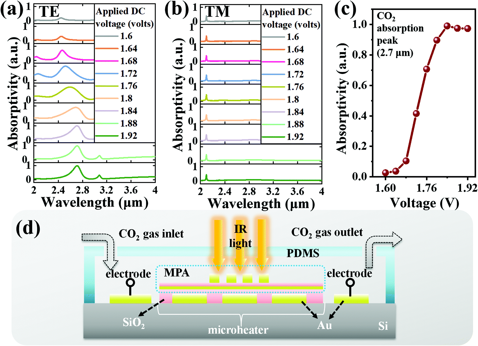
The insulator-to-metal transition of the VO2 material provides the opportunity to control the absorptivity of the MEMS-based MPA by changing the heating temperature. The absorption spectra of the MEMS-based MPA with different applied DC voltages in the TE mode are illustrated in Fig. 5(a). By driving a DC bias voltage of 1.60 volts, the temperature of the MEMS-based MPA is 351 K and the VO2 bars are operated at the insulating state. The absorptivity of ω1 resonance is 0.25 while the absorptivity of ω2 resonance is 0.15. By increasing the applied DC voltage to 1.92 volts, the temperature of the MEMS-based MPA increases to 373 K and the VO2 bars are transited to the metallic state. The absorption intensities of ω1 and ω2 resonances are enhanced to 0.99 and 0.95, respectively. Fig. 5(c) shows the non-linear relationship of the applied DC voltages and absorption intensities in the CO2 absorption spectrum (wavelength of 2.70 μm). Although many research studies have reported the optical properties of the VO2-based metamaterial at insulating and metallic states, the continuous tuning mechanism of EM characteristics has been rarely reported. The temperature of the MPA can be precisely controlled by driving a DC bias voltage on the Peano-shaped microheater, and the continuous tuning of the absorption intensity can be achieved. In addition, Fig. 5(b) shows the absorptivity of the MEMS-based MPA with different applied DC voltages in the TM mode. The absorption intensity is zero at a wavelength of 2.70 μm, which means that the absorption ability of the proposed MEMS-based MPA to CO2 inherent resonance is mainly contributed by the incident TE resonances. The proposed MEMS-based MPA shows the perfect absorption characteristic to detect CO2 gas in the TE mode. It is suitable to be used as a high-efficiency CO2 gas sensor. Fig. 5(d) shows the schematic drawing of the MEMS-based MPA for the CO2 gas molecule sensing function. The MEMS-based MPA device can be encapsulated in a microfluidic channel and injected with CO2 gas. Therefore, the incident IR light is absorbed by CO2 gas molecules. The proposed MPA exhibits absorption characteristic in the CO2 absorption spectrum, i.e., at a wavelength of 2.70 μm. When the concentration of CO2 gas is low in the surrounding environment, the maximum energy of incident IR light is absorbed by the MPA. When the concentration of CO2 gas is high, the incident IR light is decayed and the absorption intensity of the MPA becomes weak. Such absorbed optical energy is generated by the resonance of the MPA and then converted into thermal energy, which can be detected by an external thermopile. In addition, by applying different DC voltages on the microheater, the absorption capability and the detected signal at the operated wavelength can be switched. The difference in the switchable signals can be calculated and exploited to improve the efficiency of the CO2 sensor while the noise at the other wavelengths is filtered. While the thermal tuning method lacks the compatibility with electronic devices, the device is designed to provide precise voltage-controllable characteristics. Since the existing CO2 sensors are limited by the large size and cannot serve the requirement of high integration, the proposed designs can undergo miniaturization and can be integrated into electronic devices to realize high-efficient CO2 sensing application. Moreover, the MEMS-based MPA can be designed to operate at different IR wavelength ranges to detect other gas molecules as shown in Fig. 2.
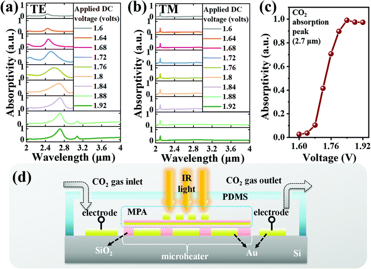 |
| | Fig. 5 Absorptivity of the MEMS-based MPA with different applied DC voltages in (a) TE and (b) TM modes. (c) The relationship of applied DC voltages and absorption intensities at a wavelength of 2.70 μm. (d) Schematic drawing of the MEMS-based MPA for the CO2 gas molecule sensing function. | |
4. Conclusion
In conclusion, an actively tunable metadevice is proposed by integrating an H-shaped MPA and MEMS-based microheater to form the MEMS-based MPA for CO2 sensing application. The microheater is patterned by using mathematical fractal theory and named the Peano-shaped microheater to provide high heating temperature and high uniformity of surface temperature. The heat is generated and then flows to the top H-shaped MPA by driving a DC bias voltage on the Peano-shaped microheater. By exploiting the insulator-to-metal transition characteristic of the VO2 material, the VO2 based H-shaped MPA can be tuned at a wavelength of 2.70 μm precisely. It is suitable to be used as a CO2 gas sensor with high sensitivity. The proposed MEMS-based MPA could be further used as an IR optoelectronic device in widespread applications, such as optical switches, tunable perfect absorbers, VOAs, and polarizers.
Author contributions
X. X. and R. X. contributed equally to this work. X. X., R. X., and Y.-S. L. conducted the methodology. X. X. and R. X. conducted the analysis with software and experiment. R. X. drew the schematic diagrams in the paper. X. X. and R. X. led the writing of original draft preparation. X. X. and Y.-S. L. led the review and editing of the paper. All authors discussed the results and commented on the manuscript.
Conflicts of interest
The authors declare no conflicts of interest.
Acknowledgements
The authors acknowledge the financial support from the Natural Science Foundation of Basic and Applied Foundation of Guangdong Province (2021A1515012217), the National Key Research and Development Program of China (2019YFA0705004), and the National Natural Science Foundation of China (11690031), and the State Key Laboratory of Optoelectronic Materials and Technologies of Sun Yat-Sen University for allowing the use of experimental equipment.
References
- N. I. Landy, S. Sajuyigbe, J. J. Mock, D. R. Smith and W. J. Padilla, Phys. Rev. Lett., 2008, 100, 207402 CrossRef CAS PubMed.
- C. M. Watts, X. L. Liu and W. J. Padilla, Adv. Mater., 2012, 24, 98–120 Search PubMed.
- W. Li, U. Guler, N. Kinsey, G. V. Naik, A. Boltasseva, J. G. Guan, V. M. Shalaev and A. V. Kildishev, Adv. Mater., 2014, 26, 7959 CrossRef CAS PubMed.
- Y. X. Cui, Y. R. He, Y. Jin, F. Ding, L. Yang, Y. Q. Ye, S. M. Zhong, Y. Y. Lin and S. L. He, Laser Photonics Rev., 2014, 8, 495–520 CrossRef CAS.
- X. Zhang, K. Chen, Y.-S. Lin and B.-R. Yang, Opt. Mater., 2021, 122, 111679 CrossRef.
- X. Xu, Y.-S. Lin, R. Fang and B.-R. Yang, Opt. Mater. Express, 2021, 11(10), 3577–3586 CrossRef CAS.
- Y.-S. Lin, J. Dai, Z. Zeng and B.-R. Yang, Nanoscale Res. Lett., 2020, 15, 77 CrossRef CAS PubMed.
- Y. Han, J. Lin and Y.-S. Lin, Opt. Lett., 2020, 45(24), 6619–6622 CrossRef PubMed.
- F. Zhan and Y.-S. Lin, Opt. Lett., 2020, 45(13), 3633–3636 CrossRef PubMed.
- D. Zheng and Y.-S. Lin, Adv. Mater. Technol., 2020, 5, 202000584 Search PubMed.
- Z. Q. Du, J. G. Liang, T. Cai, X. Wang, Q. D. Zhang, T. W. Deng, B. R. Wu, R. Q. Mao and D. P. Wang, Opt. Express, 2021, 29, 6434–6444 CrossRef PubMed.
- R. Xu, X. Liu and Y.-S. Lin, Results Phys., 2019, 13, 102176 CrossRef.
- R. Xu and Y.-S. Lin, Opt. Lett., 2018, 43, 4783–4786 CrossRef CAS PubMed.
- R. Xu, J. Luo, J. Sha, J. Zhong, Z. Xu, Y. Tong and Y.-S. Lin, Appl. Phys. Lett., 2018, 113, 101907 CrossRef.
- Z. H. Jiang, S. Yun, F. Toor, D. H. Werner and T. S. Mayer, ACS Nano, 2011, 5, 4641–4647 CrossRef CAS PubMed.
- A. Lochbaum, Y. Fedoryshyn, A. Dorodnyy, U. Koch, C. Hafner and J. Leuthold, ACS Photonics, 2017, 4, 1371–1380 CrossRef CAS.
- D. Hasan and C. Lee, Adv. Sci., 2018, 5, 1700581 CrossRef PubMed.
- A. Lochbaum, A. Dorodnyy, U. Koch, S. M. Koepfli, S. Volk, Y. Fedoryshyn, V. Wood and J. Leuthold, Nano Lett., 2020, 20, 4169–4176 CrossRef CAS PubMed.
- T. Beni, N. Yamasaku, T. Kurotsu, N. To, S. Okazaki, T. Arakawa, A. Balcytics, G. Seniutinas, S. Juodkazis and Y. Nishijima, ACS Sens., 2019, 4, 2389–2394 CrossRef CAS PubMed.
- P. Pitchappa, C. P. Ho, P. Kropelnicki, N. Singh, D. L. Kwong and C. Lee, Appl. Phys. Lett., 2014, 104, 201114 CrossRef.
- R. Xu and Y.-S. Lin, Nano Lett., 2021, 21(7), 3205–3210 CrossRef CAS PubMed.
- F. Zhu and Y.-S. Lin, Opt. Laser Technol., 2021, 134, 106635 CrossRef CAS.
- T. Xu, R. Xu and Y.-S. Lin, Results Phys., 2020, 19, 103638 CrossRef.
- R. Xu, X. Xu, B.-R. Yang, X. Gui, Z. Qin and Y.-S. Lin, Photonics Res., 2021, 9(7), 1409–1415 CrossRef.
- H. Wang, Y. Yang and L. P. Wang, Appl. Phys. Lett., 2014, 105, 071907 CrossRef.
- L. Yang, P. H. Zhou, T. X. Huang, G. S. Zhen, L. Zhang, L. Bi, X. L. Weng, J. L. Xie and L. J. Deng, Opt. Mater. Express, 2017, 7, 2767–2776 CrossRef CAS.
- G. Dayal, X. Y. Chin, C. Soci and R. Singh, Adv. Opt. Mater., 2017, 5, 1600559 CrossRef.
- K. V. Sreekanth, R. Medwal, Y. K. Srivastava, M. Manjappa, R. S. Rawat and R. Singh, Nano Lett., 2021, 21(23), 10070–10075 CrossRef CAS PubMed.
- K. V. Sreekanth, C. M. Das, R. Medwal, M. Mishra, Q. L. Ouyang, R. S. Rawat, K. T. Yong and R. Singh, Adv. Mater., 2021, 33, 2006926 CrossRef CAS PubMed.
- K. V. Sreekanth, M. ElKabbash, R. Medwal, J. H. Zhang, T. Letsou, G. Strangi, M. Hinczewski, R. S. Rawat, C. L. Guo and R. Singh, ACS Photonics, 2019, 6, 1610–1617 CrossRef CAS PubMed.
- K. V. Sreekanth, S. Han and R. Singh, Adv. Mater., 2018, 30(21), 1706696 CrossRef PubMed.
- K. V. Sreekanth, S. Sreejith, S. Han, A. Mishra, X. X. Chen, H. D. Sun, C. T. Lim and R. Singh, Nat. Commun., 2018, 9, 369 CrossRef PubMed.
- T. L. Wang, Y. P. Zhang, H. Y. Zhang and M. Y. Cao, Opt. Mater. Express, 2020, 10, 369–386 CrossRef CAS.
- X. M. Tian and Z. Y. Li, Plasmonics, 2018, 13, 1393–1402 CrossRef CAS.
- R. Z. Sun, P. H. Zhou, W. S. Ai, Y. N. Liu, Y. Li, R. M. Jiang, W. X. Li, X. L. Weng, L. Bi and L. J. Deng, Opt. Express, 2019, 27, 11537–11546 CrossRef CAS PubMed.
- C. Y. Peng, K. Ou, G. H. Li, X. Y. Li, W. J. Wang, Z. Y. Zhao, X. S. Chen and W. Lu, Opt. Express, 2020, 28, 11721–11729 CrossRef CAS PubMed.
- D. Li, H. L. Huang, H. Xia, J. P. Zeng, H. J. Li and D. Xie, Results Phys., 2018, 11, 659–664 CrossRef.
- W. V. Hans, A. S. Barker and C. N. Berglund, Phys. Rev., 1968, 40(4), 737 Search PubMed.
- D. R. Smith, D. C. Vier, T. Koschny and C. M. Soukoulis, Phys. Rev. E: Stat., Nonlinear, Soft Matter Phys., 2005, 71, 036617 CrossRef CAS PubMed.
- H. Kim, K. Cheung, R. C. Y. Auyeung, D. E. Wilson, K. M. Charipar, A. Pique and N. A. Charipar, Sci. Rep., 2019, 9, 11329 CrossRef PubMed.
Footnote |
| † These authors contributed equally. |
|
| This journal is © The Royal Society of Chemistry 2022 |
Click here to see how this site uses Cookies. View our privacy policy here. 
 *
*