
 Open Access Article
 This Open Access Article is licensed under a
 Creative Commons Attribution 3.0 Unported Licence
Growth and analysis of the tetragonal (ST12) germanium nanowires†
Adrià
Garcia-Gil
 ab,
Subhajit
Biswas
*ab,
Ahin
Roy
c,
Dzianis
Saladukh
d,
Sreyan
Raha
e,
Thomas
Blon
f,
Michele
Conroy
gh,
Valeria
Nicolosi
c,
Achintya
Singha
e,
Lise-Marie
Lacroix
f and
Justin D.
Holmes
ab
ab,
Subhajit
Biswas
*ab,
Ahin
Roy
c,
Dzianis
Saladukh
d,
Sreyan
Raha
e,
Thomas
Blon
f,
Michele
Conroy
gh,
Valeria
Nicolosi
c,
Achintya
Singha
e,
Lise-Marie
Lacroix
f and
Justin D.
Holmes
ab
aSchool of Chemistry & Tyndall National Institute, University College Cork, Cork, T12 YN60, Ireland. E-mail: s.biswas@ucc.ie; Tel: +353 (0)21 4905143
bAMBER Centre, Environmental Research Institute, University College Cork, Cork, T23 XE10, Ireland
cSchool of Chemistry and CRANN & AMBER Centre, Trinity College Dublin, Dublin 2, Ireland
dDepartment of Photonics, Tyndall National Institute, University College Cork, Cork, Ireland
eDepartment of Physics, Bose Institute, 93/1, A.P.C Road, Kolkata, 700009, India
fUniversité de Toulouse, UMR 5215 INSA, CNRS, UPS, Laboratoire de Physique et Chimie des Nano-Objets, 135 avenue de Rangueil, F-31077 Toulouse cedex 4, France
gDepartment of Materials, Royal School of Mines, Imperial College London, UK
hTEMUL, Department of Physics, Bernal Institute, University of Limerick, Limerick, V94 T9PX, Ireland
First published on 17th January 2022
Abstract
New semiconducting materials, such as state-of-the-art alloys, engineered composites and allotropes of well-established materials can demonstrate unique physical properties and generate wide possibilities for a vast range of applications. Here we demonstrate, for the first time, the fabrication of a metastable allotrope of Ge, tetragonal germanium (ST12-Ge), in nanowire form. Nanowires were grown in a solvothermal-like single-pot method using supercritical toluene as a solvent, at moderate temperatures (290–330 °C) and a pressure of ∼48 bar. One-dimensional (1D) nanostructures of ST12-Ge were achieved via a self-seeded vapour–liquid–solid (VLS)-like paradigm, with the aid of an in situ formed amorphous carbonaceous layer. The ST12 phase of Ge nanowires is governed by the formation of this carbonaceous structure on the surface of the nanowires and the creation of Ge–C bonds. The crystalline phase and structure of the ST12-Ge nanowires were confirmed by X-ray diffraction (XRD), high-resolution transmission electron microscopy (HRTEM) and Raman spectroscopy. The nanowires produced displayed a high aspect ratio, with a very narrow mean diameter of 9.0 ± 1.4 nm, and lengths beyond 4 μm. The ST12-Ge nanowire allotrope was found to have a profound effect on the intensity of the light emission and the directness of the bandgap, as confirmed by a temperature-dependent photoluminescence study.
Introduction
Group IV elements such as carbon, silicon, germanium and tin can present extensive polymorphism to form many uncommon allotropes, even in nanostructure forms, besides graphite and diamond cubic (dc) crystallographic structures.1–6 These allotropes have drawn great attention because of their interesting characteristics, e.g. high packing densities,7 insulator/semiconductor behaviour,8 metallicity9 and superconductivity,8,9 and their wide range of potential applications, such as in solar cells,10,11 gate-all-around transistors,12 and superconducting devices10,13,14 In particular, germanium polymorphs exhibit attractive electronic and optical properties, especially good electrical conductivity7 and a direct and narrow bandgap.8,9Considerable effort has been made to synthesise and characterise different polymorphs of Ge, some of which are predicted to possess better energetic stabilities in comparison with the diamond cubic Ge (dc-Ge) phase.1,5,6,15–17 To date, allotropes of Ge have typically been obtained and characterised at very high pressures (in the range of from 100 to 1600 bar), both upon compression and decompression.18 When amorphous or dc-Ge is placed under high pressure (above 10 GPa in bulk, and 17 GPa for nanoscale), a new metallic β-Sn structure (I41/amd) is formed due to a phase transformation.19 However, upon release of the pressure at room temperature, β-Sn Ge does not reverse to dc-Ge form, but transforms to different metastable phases, such as the tetragonal phase (ST12-Ge or Ge-III), the body centred-cubic structure (BC8) or the rhombohedral R8 phase, and sometimes metastable phases mixed with dc-Ge.7,20 Recently, bulk crystalline ST12-Ge was obtained after slow decompression from 14 GPa to atmospheric pressure.
Among all the possible crystalline Ge allotropes, most of them are thermodynamically unstable at room temperature and ambient pressure. However, ST12-Ge has become the most commonly studied Ge allotrope because of its kinetical stability at ambient conditions.21 ST12-Ge is based on a tetrahedral structure with 12 atoms per unit cell arranged to form fivefold, sixfold and sevenfold rings. Hence, ST12-Ge is expected to be semiconducting and has attracted special attention due to its potential use in electronic and energy storage applications.22,23 Also, comparisons with theoretical calculations carried out for ST12-silicon suggest that doped ST12-Ge may act as a superconductor at low temperatures.13 The initial characterisation of the optical properties of ST12-Ge, primarily theoretical, have produced contradictory results, especially in regards to its electronic band structure.21,24,25 Recent density-functional theory (DFT)-based calculations reported an indirect fundamental bandgap of 0.54 eV![[thin space (1/6-em)]](https://www.rsc.org/images/entities/char_2009.gif) 8 and 0.70 eV7 for the ST12-Ge structure, with a direct non-fundamental bandgap of 0.56 eV8 and 0.72 eV.7 A very small separation (∼20 meV compared to 140 meV for dc-cubic Ge) between the indirect (L) and direct (Γ) valleys potentially permits a direct bandgap transition in ST12-Ge through the application of external strain. Experimental reports on determining the bandgap of single-crystalline ST12-Ge are limited. A bandgap of 1.5 eV has been reported for nanocrystalline grains (3–4 nm) of ST12-Ge deposited via cluster-beam evaporation.26 Very recently, Zhao et al.7 reported an indirect bandgap of 0.59 eV and a direct optical transition of 0.74 eV for single-crystalline bulk ST12-Ge via optical absorbance and Tauc plot analysis.
8 and 0.70 eV7 for the ST12-Ge structure, with a direct non-fundamental bandgap of 0.56 eV8 and 0.72 eV.7 A very small separation (∼20 meV compared to 140 meV for dc-cubic Ge) between the indirect (L) and direct (Γ) valleys potentially permits a direct bandgap transition in ST12-Ge through the application of external strain. Experimental reports on determining the bandgap of single-crystalline ST12-Ge are limited. A bandgap of 1.5 eV has been reported for nanocrystalline grains (3–4 nm) of ST12-Ge deposited via cluster-beam evaporation.26 Very recently, Zhao et al.7 reported an indirect bandgap of 0.59 eV and a direct optical transition of 0.74 eV for single-crystalline bulk ST12-Ge via optical absorbance and Tauc plot analysis.
Besides the traditional high-pressure laboratory synthesis, a few techniques at ambient pressure, like plasma-enhanced severe plastic deformation (SPD)27 and indentation techniques28 have also been utilised to obtain ST12-Ge in bulk form. Although there have been attempts to grow ST12-Ge in bulk form, there have been no reports on synthesising one dimensional tetragonal Ge nanostructures, to keep track of the miniaturisation of Si-based nanoelectronics and to take advantage of their 1D geometry for new age field-effect transistor (FET) devices, e.g. finFET, gate-all-around (GAA) FET etc. Additionally, nanostructures of tetragonal Ge could be highly advantageous for solar power conversion and in energy storage devices such as Li-ion batteries.11,22 Although different deposition-based techniques, such as chemical vapour deposition (CVD),29 nanoindentation28,30,31 and ionised cluster beam deposition,32,33 have been useful in obtaining ST12-Ge crystals with small nanograins, true nanocrystalline samples (nanoparticles of diameter ∼6 nm) have only been obtained by thermal annealing of amorphous nanophase Ge by the naphthalide-mediated reduction of GeCl4.34 Subsequent research has also been directed towards the thermal stability23,35 of the nanograin allotrope, with little consensus on the results obtained.
Here we report the synthesis of single-crystalline ST12-Ge 1D nanostructures using a simple bottom-up synthetic method at mild growth temperature (290–330 °C) and moderate pressure (4.8 MPa or 48 bar). The ST12-Ge nanowires were grown using a single-step batch synthesis method, without the addition of a metal or metalloid growth catalyst. In situ formed Ge nanoparticles and carbonaceous compounds aided the growth of ST12-Ge nanowires. The crystalline phase of the ST12-Ge nanowires was analysed by X-ray diffraction (XRD), high-resolution transmission electron microscopy (HRTEM) and Raman spectroscopy. Photoluminescence (PL) was observed for the first time from the ST12-Ge structures, and a direct bandgap transition at low temperatures was confirmed for the ST12-Ge nanowires.
Results and discussion
Tetragonal (ST12) Ge nanowires were grown at relatively mild temperatures, between 290–330 °C, in a batch reactor using low boiling point solvents, e.g. toluene and the commercially available Ge precursor, diphenylgermane (DPG) (see ESI for detail synthesis method†). The in situ generated pressure in the batch reaction chamber is around ∼48 bar. The supercritical toluene environment created in the closed-cell reactors provided ideal conditions for fast precursor decomposition and in situ formation of a carbonaceous layer on the surface of the nanowires, which was crucial for the self-seeded growth of the ST12-Ge nanowires. Fig. 1a and b show SEM images of ST12-Ge nanowires grown on a Si (100) substrate at a reaction temperature of 330 °C from a 40 and 60 mM solution of DPG in toluene, respectively. Fig. 1a shows the formation of a three-dimension (3D) sponge-like porous structure (primarily consisting of carbon as indicated in energy dispersive X-ray (EDX) analysis in Fig. S1†), like a matrix, from the micron long reticulated nanowires. The Ge nanowires assemble together to form a uniform Ge film over the Si substrates. The SEM images (see Fig. 1b and Fig. S1 in the ESI†) clearly show the formation of a 3D porous network from the interweaving nanowires, consisting of bundles of individual nanowires. Significantly, nanowire growth was also achieved at a temperature as low as 290 °C (see Fig. S1 in ESI†). The yield of nanowires varied from 0.36 to 0.51 μg mm−2, depending on the growth temperature and precursor concentration. | ||
| Fig. 1 (a) and (b) SEM micrographs of Ge nanowires grown at a temperature of 330 °C from a 40 and 60 mM DPG/toluene solution, respectively. (c) XRD pattern of a nanowire sample showing the formation of ST12-Ge crystal structure. Inset shows 2D image plate obtained from the Ge nanowires with a Co micro-source. XRD-2D detector reveals the presence of highly textured {112} ST12-Ge film. (d) Raman spectrum of ST12-Ge nanowires showing Raman modes corresponding to ST12-Ge (P4321). Inset shows peaks corresponding to C–C Raman modes. | ||
Crystalline phase and structural analysis of Ge nanowires
As the primary objective of this work was to fabricate the crystalline tetragonal ST12-Ge nanowire, XRD analysis on the as-grown samples was used to determine the phase purity and crystal structure of the nanowires. Fig. 1c shows the XRD profile from a nanowire sample grown from a 60 mM DPG/toluene solution at a reaction temperature of 330 °C. After subtracting the reflection peaks from the Si substrate (see the raw XRD patterns for ST12-Ge nanowires grown under different conditions in Fig. S2 in the ESI†), the nanowire sample exhibited a sharp peak at 33.29 which is characteristics of the {112} planes of ST12-Ge (JCPDS No. 72-1425, a = 5.93 Å and c = 6.98 Å).1,16,27,30 All the as-grown nanowire samples presented the characteristic XRD peak at ∼33° associated with the {112} crystallographic plane of the ST12-Ge structure (see Fig. S2 in the ESI†). The single peak observed in the XRD corresponds to the strongest (112) reflection from the ST12-Ge sample. Peaks corresponding to other impurity phases such as dc-Ge, crystalline GeO2 and any carbon related peak (e.g. GeC, crystalline carbon) were not detected by the XRD. Lack of presence of the other XRD peaks corresponding to ST12-Ge could be due to the anisotropy of the nanowire crystal and low yield of the samples. The nanowire film obtained is highly textured, as revealed by the fairly sharp diffraction peaks obtained on a 2D-detector (inset of Fig. 1c), while polycrystalline films usually leads to diffraction rings. The bright spots observed are characterised by a 2θ angle of 38.8° (with the Co micro source), corresponding with the (112) planes of the Ge ST12 structure. Due to the parallel nature of the microsource used, they could only be detected when the sample was slightly tilted, revealing a highly texture films with a small disorientation (∼2°) compared with the Si substrate. Thus, a single sharp XRD peak could arise from the highly-crystalline nanowires lying flat (i.e. like a 〈112〉 directed thin film) on their high surface area facet (i.e. (112) in our case) on the Si substrate. To omit the possibility of influence from the substrate on the XRD observations, ST12-Ge nanowires were also grown on metallic Ti substrates (XRD pattern shown in Fig. S2 in ESI†). These samples also showed a single characteristics peak ∼33° associated with ST12-Ge, without any peaks associated with dc-Ge. Although phase pure tetragonal ST12-Ge nanowires were achieved at temperatures of 330 and 290 °C, increasing the growth temperatures to 380 and 440 °C resulted in the formation of dc-Ge nanowires, as confirmed by the Raman spectroscopy and XRD (Fig. S3 in ESI†). Observation of two entirely different phases of Ge at different growth temperature in the supercritical fluid batch synthesis method with the same Ge precursor (DPG) and solvent (toluene) nullify the participation of any solvent or precursor impurities in the growth of the Ge nanowires, and observation of the ST12-Ge phase.Raman spectroscopy, a powerful and non-destructive tool, was used to further confirm the ST12 phase of the Ge nanowires. Fig. 1d shows room temperature Raman spectrum recorded from the ST12-Ge nanowires. The measurements were performed at a low laser power (0.02 mW) to avoid laser-induced heating. The ST12 phase of Ge has a P43212 crystal structure and group theory analysis suggests that this phase has 4A1 + 5B1 + 4B2 + 8E Raman active optical phonon modes, while the dc-Ge phase only has one Raman active mode (E2g); which originates from a doubly degenerate LO-TO phonon.30 The Raman spectrum, from ST12-Ge nanowires, synthesised at 330 °C, displayed multiple peaks below 300 cm−1, which could be fitted with 10 Lorentzian line shapes. To obtain the best fit each spectrum was fitted five times to minimize errors in the peak positions. In comparison, dc-Ge nanowires of similar diameter (grown at 440 °C) depicted only a single E2g Raman mode near 300 cm−1 (Fig. S3 in ESI†). The peaks corresponding to the ST12-Ge nanowires are in general agreement with the previously reported, both calculated and experimental, Raman data for ST12-Ge.7,36 The experimental Raman modes match very well with DFT calculated Raman active modes31 of ST12-Ge, with the clear appearance of peaks corresponding to B1, A1 and E Raman modes. No peaks corresponding to dc-Ge further demonstrates the formation of phase-pure ST12-Ge nanowires at a growth temperature of 330 °C. The broadness and shift in the position of the Raman modes are possibly caused by phonon confinement in the very thin (∼9 nm) nanowires and anisotropy in the one-dimensional crystal. Additionally, sharp peaks corresponding to C–C Raman modes, observed around 1500 cm−1, indicate the presence of a carbonaceous structure in the nanowire sample (inset of Fig. 1d). For example, the peak around 1580 cm−1 corresponds to the C–C G-band.
Chemical analysis of ST12-Ge nanowires
The chemical purity of the Ge nanowires was further characterised by EDX analysis, which confirmed that the bulk of the nanowires was solely comprised of Ge atoms (see Fig. S4 in ESI†). The pure Ge composition was consistent throughout the nanowire body; as verified by EDX elemental mapping. The chemical nature of the ST12-Ge nanowires and the nanowire surface was further analysed by Fourier transform infrared (FTIR) absorption spectroscopy and X-ray photoemission spectroscopy (XPS). Characterisation of the ST12-Ge nanowire samples via FTIR spectroscopy revealed the presence and interaction between the Ge nanowires and certain carbonaceous structures. FTIR spectra taken from ST12 nanowires samples showed absorption bands at ∼2350, ∼970, ∼890 and ∼819 cm−1 (see Fig. 2a). These bands have previously been reported and, ∼2350 and 890 cm−1 in particular, correspond to the vibration modes of C![[double bond, length as m-dash]](https://www.rsc.org/images/entities/char_e001.gif) C bonds.37 The other bands, ∼970 and ∼819 cm−1 are consistent with CO2 vibration and Ge-CH3 rocking vibrations, respectively.38 FTIR analysis, therefore, confirms the formation of a carbonaceous material in the nanowire samples. Absorption bands at ∼560, and ∼740 cm−1 were also observed in the FTIR spectra which can be assigned to the stretching modes of Ge–C37,39 bonds and a Ge–H wagging mode,40 respectively. Significantly, FTIR spectra recorded from dc-Ge nanowires grown at 440 °C depicts no peak corresponding to stretching modes of Ge–C bonds (Fig. 2a). These data not only confirm the presence of a carbonaceous matrix within the Ge nanowire sample but also suggest the interaction of this layer with the surface of the ST12-Ge nanowires.
C bonds.37 The other bands, ∼970 and ∼819 cm−1 are consistent with CO2 vibration and Ge-CH3 rocking vibrations, respectively.38 FTIR analysis, therefore, confirms the formation of a carbonaceous material in the nanowire samples. Absorption bands at ∼560, and ∼740 cm−1 were also observed in the FTIR spectra which can be assigned to the stretching modes of Ge–C37,39 bonds and a Ge–H wagging mode,40 respectively. Significantly, FTIR spectra recorded from dc-Ge nanowires grown at 440 °C depicts no peak corresponding to stretching modes of Ge–C bonds (Fig. 2a). These data not only confirm the presence of a carbonaceous matrix within the Ge nanowire sample but also suggest the interaction of this layer with the surface of the ST12-Ge nanowires.
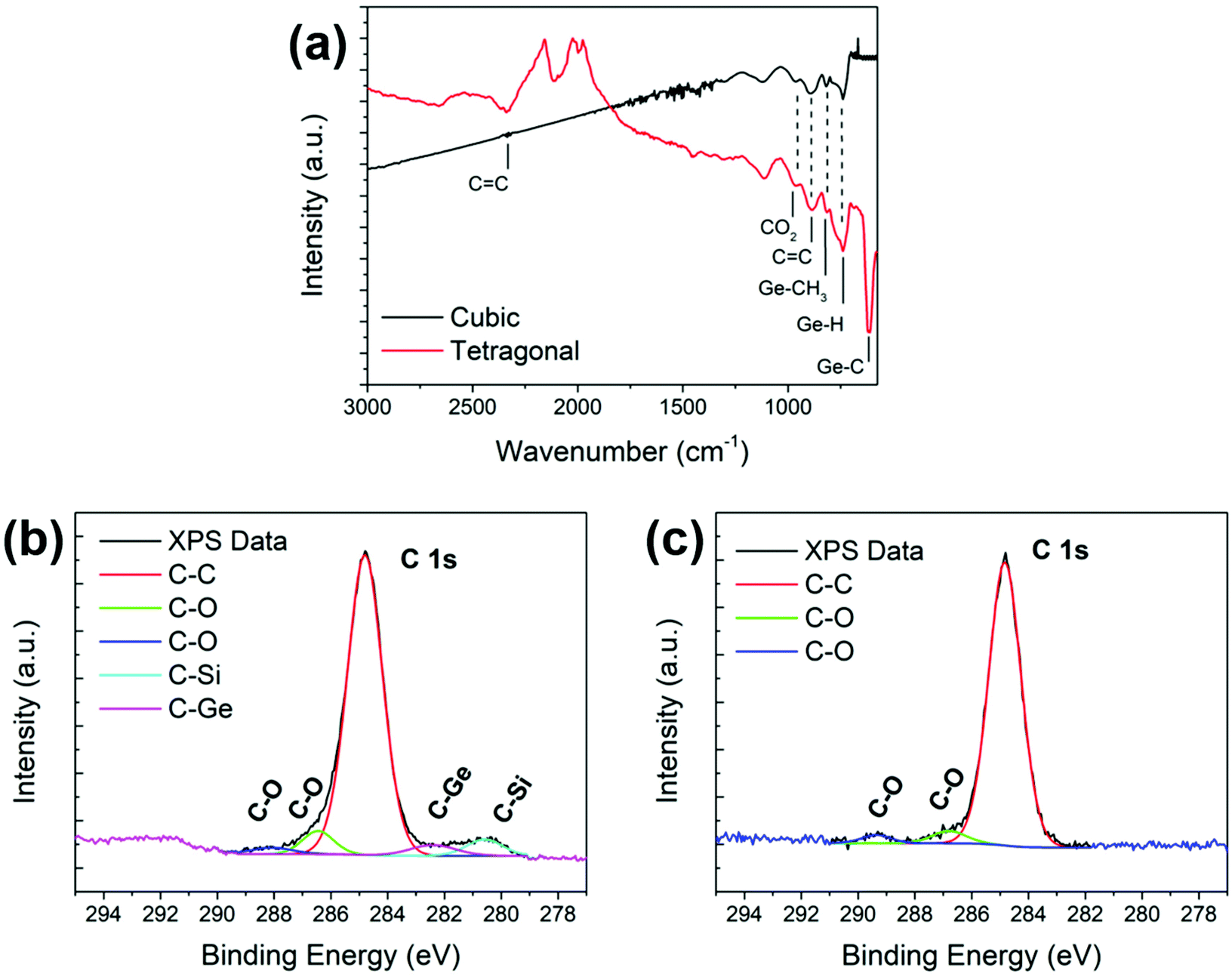 | ||
| Fig. 2 (a) FT-IR spectrum of representative ST12-Ge (grown at 330 °C) and dc-Ge (grown at 440 °C) nanowires deposited on a Si substrate. XPS spectrum of C 1s peaks from nanowires grown at (b) a reaction temperature of 330 °C and DPG concentration of 60 mM (ST12-Ge nanowires) and (c) at a reaction temperature of 440 °C and a DPG concentration of 60 mM (dc-Ge nanowires). C–Si peaks in the spectrum (b) results from the interaction of bare Si substrate with carbonaceous compounds. | ||
XPS analysis was also performed on a representative nanowire sample grown at 330 °C and a DPG concentration of 60 mM, to further study the interaction between the Ge nanowires and the as described carbonaceous structure. XPS spectra of the tetragonal ST12-Ge nanowires was compared with XPS data obtained from dc-Ge nanowires grown under similar growth condition but at the higher growth temperature of 440 °C (see Fig. 2b and c). The C 1s peak of the XPS spectrum (see Fig. 2b) of ST12-Ge and dc-Ge nanowires highlights a different interaction between the carbonaceous structures and the Ge nanowire in the two different crystal phases. The peak at ∼283.9 eV was only present in the XPS spectrum of ST12-Ge nanowires and can be assigned to a strong interaction (covalent bonding) between carbon and the surface of the ST12-Ge nanowires, i.e. Ge–C bonds (see Fig. 2b). This observation validates the FTIR data which suggests that an interaction exists between the carbonaceous matrix and the ST12-Ge nanowires (see Fig. 2a). No analogous peak was found in the XPS spectrum of dc-Ge nanowires (see Fig. 2c). C–C, CC, C–O and CO3 bonds were present in the C 1s spectrum for both samples. Germanium oxide formation was also found (see Fig. S5 in ESI†) in both samples upon exposure of the samples to air when stored in an ambient atmosphere. Thus, the carbonaceous compounds bonded to the nanowire surface could be discrete and do not act as a passivation layer to protect the Ge nanowires from oxidation. Both FTIR and XPS evaluations confirm carbonaceous compound formation in the samples and interactions between this carbonaceous matrix with the surface of the ST12-Ge nanowires.
Structural and crystal quality analysis of ST12-Ge nanowires
The surface interaction of the Ge nanowires with the carbonaceous matrix can potentially induce strain and crystal deformation, such as the formation of twins and stacking faults. HAADF-STEM, HRTEM and selected area electron diffraction (SAED) were used to further confirm the formation of the ST12-Ge crystalline phase and structural quality of the nanowires. Fig. 3a and b show HAADF-STEM data from an ST12-Ge nanowire sample grown at 330 °C from a 60 mM DPG/toluene solution. The nanowire exhibited uniform structural quality and a crystalline nature, analogous to other nanowires formed under similar growth conditions. The ST12-Ge structure had a distorted tetrahedral arrangement with a packing density about 11% greater than that of dc-Ge.21 HAADF-STEM of the Ge nanowires showed the stacking of {110} planes along the nanowire growth direction (see Fig. 3a). A more detailed examination of the nanowire crystal is depicted in the high-resolution STEM (HRSTEM) image (see Fig. 3b), oriented along the 〈110〉 zone axis, and recorded from the core of a crystalline ST12-Ge nanowire. HRSTEM imaging reveals an interplanar spacing (d) of 0.21 nm along with the nanowire growth axis, corresponding to the {220} plane of an ST12-Ge crystal. All the interplanar spacings for other crystal planes match well with ST12-Ge (JCPDS 072-1425). Fast Fourier transformation (FFT) of the HRSTEM on the single nanowire could only be indexed to the ST12-Ge structure (see Fig. 3c) and the reflections were assigned to the high-order Laue zone diffraction of {002}, {111} and {220} planes of ST12-Ge (JCPDS 072-1425). Additionally, the interplanar angles of ∼31°, ∼59° and ∼90° were measured between (111) and (220), (002) and (111), and (002) and (220), respectively. These interplanar angles match well with the tetragonal Ge crystal and are particularly useful in assigning the lattices with closely matched spacings. FFT pattern recorded from the nanowire also confirms the single-crystalline nature of the nanowires. | ||
| Fig. 3 (a) HRSTEM image of ST12-Ge nanowires with the stacking of (110) plane along the nanowire growth axis. (b) Latticed-resolved HRSTEM image of an ST12-Ge nanowire. (c) FFT pattern recorded from the representative ST12-Ge nanowire (part (a)) which confirms the ST12 structure and nanowire growth direction. (d) Diameter distributions of Ge nanowires obtained at 330 °C from a 60 mM DPG/toluene solution. (e) HRTEM image of a Ge seed and nanowire interface (shown by the red box on the top-left inset) confirms the self-seeded growth. Top-right inset shows an FFT of the seed area. | ||
The presence of the amorphous carbon on the surface of the nanowires was observed by TEM to be a discontinuous and uneven coating along the length of the nanowires (see Fig. S6 in ESI†). Thus the carbonaceous coating on the nanowires does not protect the nanowires from surface oxidation, as seen from the XPS spectra (Fig. S5 in the ESI†). ST12-Ge nanowires are very thin with a narrow diameter distribution, mean diameter of 9.0 (± 1.4) nm (Fig. 3d). The mean diameter of the Ge nanowires was found to be uniform for all growth conditions and much below the Bohr radius (∼24.3 nm) of Ge. Most of the nanowires exceeded a measurable length over 4 μm and very few displayed kinking at the growth temperatures employed. Tapered nanowires were also not observed under any growth conditions investigated. The presence of the hemispherical seed and the seed-nanowire interface was examined by HRTEM (see Fig. 3e). A low-magnification TEM image of a Ge nanowire with a dark contrasted growth seed can be seen in the inset of Fig. 3e (additional TEM and STEM images of nanowires with Ge seeds are shown in Fig. S7 in ESI†). Fig. 3e shows an HRTEM image recorded with 〈110〉 zone axis alignment, from the same nanowire. Fast Fourier Transform (FFT), in the top-right inset of Fig. 3e, of the seed region also confirms the formation of crystalline ST12-Ge. The crystal structure in both the nanoparticle and the nanowire segments correspond to ST12-Ge, which confirms the participation of a self-seeded, bottom-up growth with the ST12-Ge nanoparticle seed.41–43 Self-seeding growth of nanowires was further confirmed with EDX analysis from the nanowire tips (Fig. S7a in the ESI†), showing only the presence of Ge.
Growth mechanism of ST12-Ge nanowires
The growth of the self-seeded ST12-Ge nanowires likely occurs via a triple-phase (source-seed-nanowire) bottom-up growth which is aided by the formation of the carbonaceous matrix (a schematic of the growth is shown in Fig. 4). The formation of Ge seeds and their participation in nanowire growth (self-seeded) is evident from the presence of Ge nanoparticles at the tips of the nanowires (see Fig. 3e and S7†). In self-catalytic growth, temperature and pressure are key factors associated with the Ge precursor decomposition and nanowire growth. In our experiments, ST12-Ge nanowires were only synthesised under certain temperatures (290 and 330 °C) and pressure (an in situ generated pressure of ∼48 bar) conditions, close to the critical point of pure toluene (318.6 °C and 41.3 bar). These reaction conditions give the necessary environment to generate ST12-Ge nanoparticles which act as the catalytic seed for ST12-Ge nanowire growth (Fig. S7c in the ESI†). The formation of the nanoparticle phase takes place when the Ge precursor (DPG) decomposes to form Ge adatoms, liberating very reactive phenyl groups.44 GC-MS analysis (see Fig. S7d in ESI†) of the reactant solution revealed the by-products of the reaction as diphenylmethane and derivatives, e.g. 2,3′-dimethyl-1,1′-byphenyl, bybenzyl or 1-methyl(4-phenylmethyl)benzene, along with toluene (and derivatives), and tetraphenylgermane. Under supercritical conditions in a closed cell, the phenyl-based long-chain molecules, e.g. diphenylmethane and derivatives, start polymerising45 and precipitate over the available surfaces (sample substrate and reactor's walls). Of note, self-seeded nanowire growth was not observed under flow-through supercritical fluid reaction conditions. Instead, large spherical particles of Ge via homogeneous nucleation and Ostwald ripening were observed. This could be due to the large localised concentration of diphenylmethane and derivatives, in respect to the Ge adatom concentration, in the batch reaction process compared to a flow-through reaction.46,47 | ||
| Fig. 4 Illustration of the proposed ‘self-seeded’ ST12-Ge nanowire growth mechanism. Stage I corresponds to precursor decomposition and polymerisation of the liberated phenyl groups. Stage II consists of aggregation and nanoparticle formation from the available Ge adatoms. Eventually, stage III represent nucleation and growth of ST12-Ge nanowires from the outer disposed Ge nanoparticle seeds. | ||
The formation of Ge nanoparticles seeds for nanowire growth can be described as a spontaneous phenomenon. At this point, available Ge adatoms, via the decomposition of DPG, aggregates and dissolves into the carbonaceous matrix to form the Ge nanoparticles. The as-formed organic structures limit the capacity of aggregation and Ostwald ripening of the Ge nanoparticles and thus the formation of larger spherical particles. Ge nanoparticles placed at the outer surface of the polymer are exposed for the attachment of Ge adatoms for the growth of Ge nanowires. Self-seeded growth of Ge nanowires from in situ generated nanoparticles has previously been proposed via “pseudo” VLS-like growth.42,45 In our particular case, the initial formation of Ge nanoparticles in the carbonaceous template (see Fig. S7 in ESI†) and the presence of these nanoparticles at the tips of the nanowires, indicates the participation of nanoparticle seeds in the growth of the ST12-Ge nanowires. Of note, the elemental, structural and chemical analysis did not indicate any presence of metal (or semimetal) impurities which can participate (in a three-phase growth paradigm) in the seedless growth of Ge nanowires. Additionally, solvents and precursors were also sourced from different suppliers (Sigma-Aldrich, ABCR-GmbH, Flurochem, Merck) to nullify any influence of impurities on the seedless nanowire growth. Synthesis with precursors and solvents sourced from different suppliers resulted in the growth of Ge nanowires with similar morphologies and ST12 phase, also confirming the reproducibility of the synthetic method.
The formation of the carbonaceous structure on the Ge nanowires and its interaction with the Ge is likely to be key to the observation of ST12-Ge over dc-Ge crystalline structure under certain growth conditions. In nanowires, due to the high surface to volume ratio, surface energy plays a crucial role in the formation and stability of the metastable nanostructure, particularly in the case of nanostructure with small radii. The nanowire diameter and its specific sidewall facets have been often pointed out as key factors determining the crystal phase of nanowires.48 The energy difference between dc-Ge and ST12-Ge structures gets significantly small for nanostructures.49,50 The energy difference between the two phases further decreases with the change in the surface properties, e.g. reconstructed surface, of the nanostructures.50 The chemical interaction at the surface plays a key role in the stability of the ST12 phase in nanostructures.50 The formation of metastable tetragonal clusters is possible by trapping Ge nanoparticles with carbon resulting in unsaturated and reconstructed surfaces at low temperatures. Thus, along with the nanowire diameter (diameter of ∼9 nm for ST12-Ge nanowires), the formation of singular carbonaceous-structure compositions and their interaction with the available Ge surface (FTIR and XPS analysis of ST12-Ge nanowires, Fig. 2) could be crucial in determining the phase and the stability of the ST12-Ge nanowire phase. As the cubic and ST12-Ge nanostructures have comparable lattice energies, their nucleation is likely dependent on local environmental factors such as growth temperature and pressure.
Surface tension could also be a key contributor to the persistence of the ST12 phase in Ge nanostructures. Kim et al.34 suggested that the addition of the sterically hindered organometallic reagent t-BuMgCl promotes the nucleation of ST12 structures in Ge nanoparticles by imparting surface strain onto nascent amorphous Ge nanoclusters which results in a metastable surface with a high degree of unsaturation that leads to an ST12-Ge structure. In our case, ST12-Ge nanowires are only obtained at growth temperatures between 290 and 330 °C, whereas dc-Ge or a mixed phase was obtained at higher temperatures. Also having DPG concentrations of 40 and 60 mM at this temperatures in the batch synthesis is critical to obtain the ST12 phase of Ge nanowires (Fig. S1†). An interaction between the Ge and the carbonaceous compound was only observed, with the formation of the Ge–C bond, for the ST12-Ge nanowires (see Fig. 2a and b). Osten et al.51 have previously postulated that a small amount of isoelectronic carbon (<2 at%) can induce strain in the SiGe lattice for a tetragonal distortion. The formation of the Ge–C bond at the surface of the Ge nanowires can therefore potentially induce strain in the Ge lattice due to the change in the bonding environment, the bond length of Ge–C 1.98 Å and Ge–Ge 2.46 Å. This strain can change the Ge–Ge bond length and angular distortion in the lattice and create a tetragonal symmetry in the nanowires. Additionally, the surface stress, which can be induced by the carbonaceous matrix, can act as the driving force by creating a compressive strain in a certain crystal direction, e.g. [001], for the phase transformation.52 Thus, the presence of the carbonaceous matrix and the Ge–C bond formation at the surface of the Ge nanowire plays a crucial role in the formation of the ST12 phase. A detailed exploration on the exact role of the carbon in the formation of ST12-Ge by high resolution strain mapping and tomography is delegated to a later study.
Photoluminescence of ST12-Ge nanowires
Photoluminescence (PL) is a primary technique to determine the nature of the bandgap in nanoscale systems. PL peak positions, intensity and linewidths can be used to determine the nature of an electronic band transition. Previous attempts to obtain detectable PL signals in the near-infrared (NIR) region of the spectrum from the ST12-Ge crystals were not successful for both room temperature and low-temperature measurements.33,34 To examine the nature of the band transition in ST12 nanowires, low-temperature PL studies were carried out using a liquid helium cryostat using a Ti:Sa laser with an excitation wavelength of 700 nm. A PL spectrum recorded from ST12-Ge nanowires recorded at 10 K is depicted in Fig. 5a. The PL spectrum shows an intense PL peak centred at 1938 nm, which equates to bandgap energy of 0.64 eV. By fitting the spectra to the Gauss function, the full width half maximum (FWHM) of the peak was obtained. The primary emission peak has a linewidth of 362 nm. The PL peak position of the ST12-Ge (0.64 eV) reported here matches well with the theoretically calculated bandgap for ST12-Ge.7,53 Zhao et al.7 and Malone et al.8 have calculated, by DFT using a hybrid functional approach, the fundamental bandgap of bulk ST12-Ge to be indirect with values of 0.70 and 0.54 eV respectively. However, their calculation also predicted a relatively “weak” indirect bandgap for ST12-Ge, in the sense that the direct bandgap is only ∼20 meV (compared to 140 meV for dc-Ge) larger than the indirect bandgap. Experimental determination of the bandgap of ST12-Ge is rarely reported. A bandgap of 1.5 eV was reported for cluster beam deposited Ge nanograins through optical absorption measurements,26 whereas optical absorbance and reflectivity measurements of bulk ST12-Ge and Tauc plot analysis showed a fundamental indirect bandgap of 0.59 eV and a direct transition at 0.74 eV.7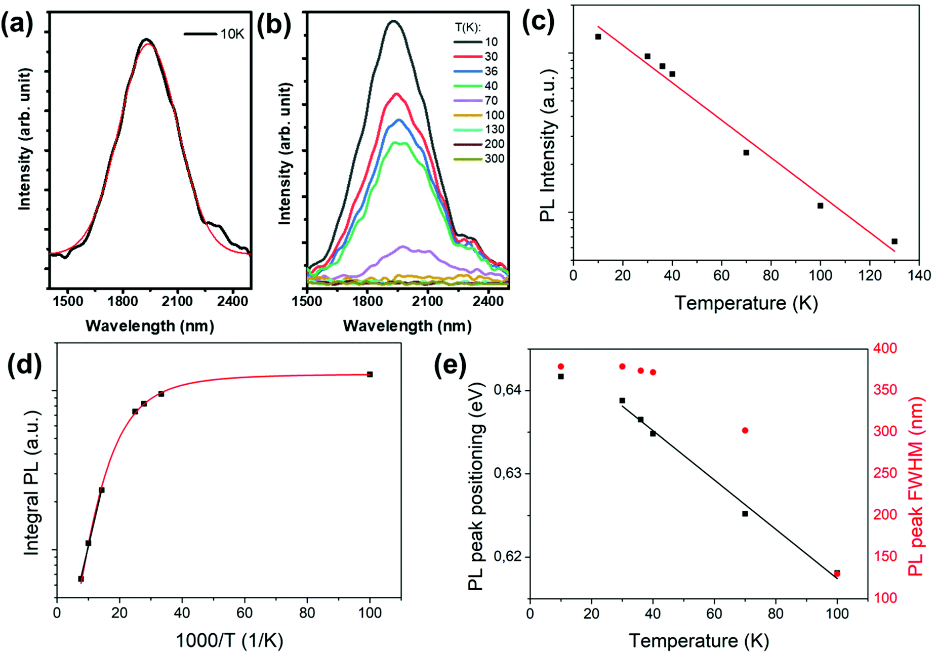 | ||
| Fig. 5 (a) PL spectra of ST12-Ge nanowires obtained at 10 K. (b) Temperature-dependent PL spectrum obtained from ST12-Ge nanowires at temperatures between 10 to 300 K. (c) Lineal fit plot of the integral PL intensity vs. temperature of the peak at ∼1940 nm from 10 to 100 K with the coefficient of determination close to unity (R2 = 0.9908). (d) The Arrhenius relation of the integral PL intensity vs. temperature of the peak at ∼1940 nm from 10 to 100 K with the coefficient of determination close to unity (R2 = 0.9774). (e) Linear fit plot (black) of the PL peak position vs. temperature of the peak at ∼1940 nm from 10 to 100 K with the coefficient of determination close to unity (R2 = 0.9936). Red dot plot corresponds to the PL peak FWHM at the different temperatures. | ||
Temperature-dependent PL studies are invaluable for probing the nature of the fundamental bandgap of a material.54,55 Temperature-dependent PL studies have previously been used to probe the direct/indirect nature of the fundamental gap in 1D nanoscale materials.56–58 PL spectra recorded as a function of temperatures are plotted in Fig. 5b, and to the best of our knowledge is the first reported experimental observation of PL from any ST12-Ge structure. The primary PL emission (∼0.64 eV at 10 K) from ST12-Ge nanowires monotonously decreases in intensity with increasing temperature (see Fig. 5b), which can be attributed to a reduced transfer of electrons from the Γ to L valleys by thermal activation, thus a higher electron population in the Γ valley. A monotonical decrease (see Fig. 5c) in the PL intensity is observed with increasing temperature, which is typical behaviour of a direct bandgap semiconductor.54,58–61 For a fundamentally indirect-bandgap semiconductor, the intensity of the primary PL peak increases with temperature as excited carriers which accumulate at the indirect band extreme at low temperature get thermally excited into the higher energy direct minimum with the increase in temperature. They recombine with a higher quantum efficiency and emit light with higher intensity at higher temperatures. On the other hand, for a direct bandgap semiconductor, with an increase in temperature the PL intensity decreases due to the increase of the non-radiative electron–hole recombination process. This also includes the fast diffusion of photocarriers toward surfaces and interfaces leading to non-radiative surface and interface recombination respectively. Thus the radiative transition rate is reduced with the activation energy EA. An Arrhenius plot, depicting integrated photoluminescence intensity as a function of inverted temperature is shown in Fig. 5d. Arrhenius plots have been fitted with a single exponential function with a coefficient of determination (R2) close to unity (R2 = 0.9774). The activation energy (EA) for the non-radiative processes from the Arrhenius plots was calculated to be 59 meV. The high activation energy for the non-radiative process at these temperatures indicates towards a strong direct bandgap transition. Furthermore, narrow linewidth deviation, determined by the FWHM when fitted with a Gaussian function, of the PL emission at low temperatures (between 362 to 300 nm for temperature between 10 to 70 K) is indicative of a single channel of recombination and thus also indicates a stronger direct bandgap transition at these temperatures.54
The effect of temperature on the peak position is displayed in Fig. 5e. The temperature dependence of the PL peak position shows an increase in bandgap energy for a decrease in temperature from 100 to 10 K. The bandgap is blue-shifted from 0.61 to 0.64 eV with the decrease in temperature. The temperature dependence of the PL peak energy can provide information on the carrier distribution within electronic bands or localised states. The monotonic decrease of the direct bandgap energy with temperature follows the bandgap (Varshni law) and carrier distribution variation in a semiconductor,62 similar to previous observations for Ge and GeSn alloys.54–56 A dominant direct bandgap transition is observed at low temperatures (below 100 K). On an important note, no emission was observed from dc-Ge nanowires grown at 440 °C with the InGaAs detector. i.e. the detector used for ST12-Ge nanowires (Fig. S8a in the ESI†). However a broad, low-intense PL spectrum centred at ∼1500 nm (∼0.80 eV) was observed from dc-Ge nanowires with a highly-sensitive (but low detection range) InAs detector. (Fig. S8b in the ESI†). Radically different PL characteristics from ST12-Ge compared to dc-Ge nanowire (of very similar morphology) provides further evidence of a different carrier recombination pathway for these two types of Ge nanowires. Although the steady-state PL measurements gave an indication on the nature of the bandgap for ST12-Ge nanowires, direct measurements of the carrier lifetimes with time-resolved photoluminescence are required in order to precisely resolve the directness of the electronic band structure in ST12-Ge nanowires, and delegated to a future study.
Conclusions
In summary, the growth of tetragonal Ge nanowires was achieved via a supercrtical fluid-assisted solvothermal-like process. ST12-Ge nanowire growth was achieved at moderate temperatures and much lower pressure (∼4 order of magnitude) compared to previously synthesised ST12-Ge bulk crystals. The formation of carbonaceous compounds on the surface of the nanowires and its interaction with the nanowire, in a batch setup, leads to the growth of this novel allotrope (ST12) of Ge in 1-D nanoform. Three-phase bottom-up growth, via in situ formed Ge growth catalysts, is liable for the 1D growth. This method opens a new window of fast, simple and accessible procedures for obtaining crystalline 0D and 1D nanostructures. Further engineering of the ST12 nanostructures, e.g. through doping, heterostructure formation, to tune the physical properties of this novel material could also be achieved via this bottom-up growth approach. PL studies suggest that the ST12-Ge nanowires possess a bandgap with direct character ∼0.64 eV. Overall, we have demonstrated that bottom-up grown ST12-Ge nanowires represent a low-cost approach to meet the growing demand for efficient group-IV nano/optoelectronic materials suitable for monolithic integration on Si.Author contributions
A. G. and S. B. contributed equally as first authors in this work. S. B., A. G. and J. D. H. designed the experiments. S. B. and A. G. conducted the experiments. S. B. and A. G. co-wrote the manuscript with all authors participated in review the manuscript. A. R., M. C. and V. N. performed the TEM and STEM experiments. A. S. and S. R. participated in Raman measurements and analysis while T. O. measured PL spectroscopy and analysed the PL data. T. B. and L. M. L. performed and analysed XRD experiments.Conflicts of interest
The authors declare no competing financial interest.Acknowledgements
This research was funded by Science Foundation Ireland (Grant No: 14/IA/2513). A part of the imaging for this project was carried out at the Advanced Microscopy Laboratory (AML) at the AMBER Centre, CRANN Institute, Trinity College Dublin, Ireland. AML is an SFI supported imaging and analysis Centre.References
- S. Biswas, J. Doherty, D. Majumdar, T. Ghoshal, K. Rahme, M. Conroy, A. Singha, M. A. Morris and J. D. Holmes, Chem. Mater., 2015, 27, 3408–3416 CrossRef CAS.
- X. Liu and D. Wang, Nano Res., 2009, 2, 575–582 CrossRef CAS.
- F. J. Lopez, U. Givan, J. G. Connell and L. J. Lauhon, ACS Nano, 2011, 5, 8958–8966 CrossRef CAS PubMed.
- A. Convertino, M. Cuscunà, G. Nicotra, C. Spinella, L. Felisari, G. Fortunato and F. Martelli, J. Cryst. Growth, 2011, 335, 10–16 CrossRef CAS.
- N. Jeon, S. A. Dayeh and L. J. Lauhon, Nano Lett., 2013, 13, 3947–3952 CrossRef CAS PubMed.
- L. Vincent, G. Patriarche, G. Hallais, C. Renard, C. Gardès, D. Troadec and D. Bouchier, Nano Lett., 2014, 14, 4828–4836 CrossRef CAS PubMed.
- Z. Zhao, H. Zhang, D. Y. Kim, W. Hu, E. S. Bullock and T. A. Strobel, Nat. Commun., 2017, 8, 1–8 CrossRef CAS PubMed.
- B. D. Malone and M. L. Cohen, Phys. Rev. B: Condens. Matter Mater. Phys., 2012, 86, 1–7 CrossRef.
- D. Selli, I. A. Baburin, R. Martoňák and S. Leoni, Sci. Rep., 2013, 3, 1466 CrossRef PubMed.
- B. D. Malone, J. D. Sau and M. L. Cohen, Phys. Rev. B: Condens. Matter Mater. Phys., 2008, 78, 161202 CrossRef.
- M. Vörös, S. Wippermann, B. Somogyi, A. Gali, D. Rocca, G. Galli and G. T. Zimanyi, J. Mater. Chem. A, 2014, 2, 9820–9827 RSC.
- K. H. Yeo, S. D. Suk, M. Li, Y. Y. Yeoh, K. H. Cho, K. H. Hong, S. K. Yun, M. S. Lee, N. Cho, K. Lee, D. Hwang, B. Park, D. W. Kim, D. Park and B. Il Ryu, in Technical Digest - International Electron Devices Meeting, IEDM, 2006 Search PubMed.
- B. D. Malone, J. D. Sau and M. L. Cohen, Phys. Rev. B: Condens. Matter Mater. Phys., 2008, 78, 035210 CrossRef.
- G. Weill, J. L. Mansot, G. Sagon, C. Carlone and J. M. Besson, Semicond. Sci. Technol., 1989, 4, 280–282 CrossRef CAS.
- A. Mujica, C. J. Pickard and R. J. Needs, Phys. Rev. B: Condens. Matter Mater. Phys., 2015, 91, 214104 CrossRef.
- Z. Zhao, F. Tian, X. Dong, Q. Li, Q. Wang, H. Wang, X. Zhong, B. Xu, D. Yu, J. He, H. T. Wang, Y. Ma and Y. Tian, J. Am. Chem. Soc., 2012, 134, 12362–12365 CrossRef CAS PubMed.
- C. J. Pickard and R. J. Needs, Phys. Rev. B: Condens. Matter Mater. Phys., 2010, 81, 014106 CrossRef.
- A. Mujica, A. Rubio, A. Muñoz and R. J. Needs, Rev. Mod. Phys., 2003, 75, 863–912 CrossRef CAS.
- A. V. Sapelkin, V. A. Karavanskii, G. Kartopu, M. Es-Souni and Z. Luklinska, Phys. Status Solidi, 2007, 244, 1376–1380 CrossRef CAS.
- F. Coppari, J. C. Chervin, A. Congeduti, M. Lazzeri, A. Polian, E. Principi and A. Di Cicco, Phys. Rev. B: Condens. Matter Mater. Phys., 2009, 80, 1–9 CrossRef.
- F. P. Bundy and J. S. Kasper, Science, 1963, 139, 340–341 CrossRef CAS PubMed.
- Y. J. Cho, H. S. Im, H. S. Kim, Y. Myung, S. H. Back, Y. R. Lim, C. S. Jung, D. M. Jang, J. Park, E. H. Cha, W. Il Cho, F. Shojaei and H. S. Kang, ACS Nano, 2013, 7, 9075–9084 CrossRef CAS PubMed.
- Y. Ikoma, T. Toyota, Y. Ejiri, K. Saito, Q. Guo and Z. Horita, J. Mater. Sci., 2015, 51, 138–143 CrossRef.
- A. Mujica and R. J. Needs, Phys. Rev. B: Condens. Matter Mater. Phys., 1993, 48, 17010–17017 CrossRef CAS PubMed.
- J. D. Joannopoulos and M. L. Cohen, Phys. Rev. B: Solid State, 1973, 7, 2644–2657 CrossRef CAS.
- S. Sato, S. Nozaki and H. Morisaki, Appl. Phys. Lett., 1998, 72, 2460–2462 CrossRef CAS.
- R. K. Islamgaliev, R. Kuzel, E. D. Obraztsova, J. Burianek, F. Chmelik and R. Z. Valiev, Mater. Sci. Eng., A, 1998, 249, 152–157 CrossRef.
- J. Il Jang, M. J. Lance, S. Wen and G. M. Pharr, Appl. Phys. Lett., 2005, 86, 1–3 Search PubMed.
- J. Jiang, K. Chen, X. Huang, Z. Li and D. Feng, Appl. Phys. Lett., 1994, 65, 1799–1801 CrossRef CAS.
- H. W. Chiu and S. M. Kauzlarich, Chem. Mater., 2006, 18, 1023–1028 CrossRef CAS.
- J. E. Bradby, J. S. Williams, J. Wong-Leung, M. V. Swain and P. Munroe, Appl. Phys. Lett., 2002, 80, 2651–2653 CrossRef CAS.
- S. Sato, S. Nozaki and H. Morisaki, J. Appl. Phys., 1997, 81, 1518–1521 CrossRef CAS.
- S. Sato, S. Nozaki, H. Morisaki and M. Iwase, Appl. Phys. Lett., 1995, 66, 3176 CrossRef CAS.
- S. J. Kim, O. K. Quy, L. S. Chang, E. A. Stach, C. A. Handwerker and A. Wei, J. Mater. Chem., 2010, 20, 331–337 RSC.
- L. Q. Huston, B. C. Johnson, B. Haberl, S. Wong, J. S. Williams and J. E. Bradby, J. Appl. Phys., 2017, 122, 175108 CrossRef.
- K. Winer and F. Wooten, Phys. Status Solidi, 1986, 136, 519–527 CrossRef CAS.
- P. Kazimierski and L. Jóźwiak, J. Non-Cryst. Solids, 2009, 355, 280–286 CrossRef CAS.
- M. Gazicki, Chaos, Solitons Fractals, 1999, 10, 1983–2017 CrossRef CAS.
- J. Q. Zhu, C. Z. Jiang, J. C. Han, H. L. Yu, J. Z. Wang, Z. C. Jia and R. R. Chen, Appl. Surf. Sci., 2012, 258, 3877–3881 CrossRef CAS.
- M. Cardona, Phys. Status Solidi, 1983, 118, 463–481 CrossRef CAS.
- R. G. Hobbs, S. Barth, N. Petkov, M. Zirngast, C. Marschner, M. A. Morris and J. D. Holmes, J. Am. Chem. Soc., 2010, 132, 13742–13749 CrossRef CAS PubMed.
- O. Lotty, R. Hobbs, C. O'Regan, J. Hlina, C. Marschner, C. O'Dwyer, N. Petkov and J. D. Holmes, Chem. Mater., 2013, 25, 215–222 CrossRef CAS.
- S. Connaughton, R. Hobbs, O. Lotty, J. D. Holmes and V. Krstić, Adv. Mater. Interfaces, 2015, 2, 1400469 CrossRef.
- A. M. Chockla and B. A. Korgel, J. Mater. Chem., 2009, 19, 996–1001 RSC.
- N. Zaitseva, J. Harper, D. Gerion and C. Saw, Appl. Phys. Lett., 2005, 86, 1–3 CrossRef.
- T. Hanrath and B. A. Korgel, Adv. Mater., 2003, 15, 437–440 CrossRef CAS.
- S. Biswas, A. Singha, M. A. Morris and J. D. Holmes, Nano Lett., 2012, 12, 5654–5663 CrossRef CAS PubMed.
- J. Yu, C. Zhang, W. Wu, Y. Cai and Y. Zhang, Appl. Surf. Sci., 2021, 548, 148944 CrossRef CAS.
- H. W. Chiu, C. N. Chervin and S. M. Kauzlarich, Chem. Mater., 2005, 17, 4858–4864 CrossRef CAS.
- L. Pizzagalli, J. E. Klepeis and F. Gygi, Phys. Rev. B: Condens. Matter Mater. Phys., 2001, 63, 165324 CrossRef.
- H. J. Osten, E. Bugiel and P. Zaumseil, Appl. Phys. Lett., 1994, 64, 3440–3442 CrossRef CAS.
- J. Diao, K. Gall and M. L. Dunn, Nat. Mater., 2003, 2, 656–660 CrossRef CAS PubMed.
- M. Khazaei, Y. Liang, N. S. Venkataramanan and Y. Kawazoe, Phys. Rev. B: Condens. Matter Mater. Phys., 2012, 85, 054101 CrossRef.
- D. Stange, S. Wirths, N. Von Den Driesch, G. Mussler, T. Stoica, Z. Ikonic, J. M. Hartmann, S. Mantl, D. Grützmacher and D. Buca, ACS Photonics, 2015, 2, 1539–1545 CrossRef CAS.
- M. Y. Ryu, T. R. Harris, Y. K. Yeo, R. T. Beeler and J. Kouvetakis, Appl. Phys. Lett., 2013, 102, 1–5 Search PubMed.
- S. Manna, A. Katiyar, R. Aluguri and S. K. Ray, J. Phys. D: Appl. Phys., 2015, 48, 215103 CrossRef.
- J. Doherty, S. Biswas, D. Saladukha, Q. Ramasse, T. S. Bhattacharya, A. Singha, T. J. Ochalski and J. D. Holmes, J. Mater. Chem. C, 2018, 6, 8738–8750 RSC.
- S. Biswas, J. Doherty, D. Saladukha, Q. Ramasse, D. Majumdar, M. Upmanyu, A. Singha, T. Ochalski, M. A. Morris and J. D. Holmes, Nat. Commun., 2016, 7, 114005 Search PubMed.
- I. G. Lezama, A. Arora, A. Ubaldini, C. Barreteau, E. Giannini, M. Potemski and A. F. Morpurgo, Nano Lett., 2015, 15, 2336–2342 CrossRef CAS PubMed.
- S. Wirths, R. Geiger, N. Von Den Driesch, G. Mussler, T. Stoica, S. Mantl, Z. Ikonic, M. Luysberg, S. Chiussi, J. M. Hartmann, H. Sigg, J. Faist, D. Buca and D. Grützmacher, Nat. Photonics, 2015, 9, 88–92 CrossRef CAS.
- E. M. T. Fadaly, A. Dijkstra, J. R. Suckert, D. Ziss, M. A. J. van Tilburg, C. Mao, Y. Ren, V. T. van Lange, K. Korzun, S. Kölling, M. A. Verheijen, D. Busse, C. Rödl, J. Furthmüller, F. Bechstedt, J. Stangl, J. J. Finley, S. Botti, J. E. M. Haverkort and E. P. A. M. Bakkers, Nature, 2020, 580, 205–209 CrossRef CAS PubMed.
- Y. P. Varshni, Physica, 1967, 34, 149–154 CrossRef CAS.
Footnote |
| † Electronic supplementary information (ESI) available: SEM of all the ST12-Ge nanowires screened growth conditions; SEM, Raman and XRD of dc-Ge nanowires; EDX of ST12-Ge nanowires; XPS and GC-MS spectra of ST12-Ge nanowires; STEM of ST12-Ge nanowires; HRSTEM, PL of dc-Ge nanowires. See DOI: 10.1039/d1nr07669h |
| This journal is © The Royal Society of Chemistry 2022 |