
 Open Access Article
 This Open Access Article is licensed under a
 Creative Commons Attribution 3.0 Unported Licence
Transferable single-layer GeSn nanomembrane resonant-cavity-enhanced photodetectors for 2 μm band optical communication and multi-spectral short-wave infrared sensing†
Qimiao
Chen
 *a,
Shaoteng
Wu
*ab,
Lin
Zhang
a,
Hao
Zhou
a,
Weijun
Fan
a and
Chuan Seng
Tan
ac
*a,
Shaoteng
Wu
*ab,
Lin
Zhang
a,
Hao
Zhou
a,
Weijun
Fan
a and
Chuan Seng
Tan
ac
aSchool of Electrical and Electronic Engineering, Nanyang Technological University, Singapore 639798. E-mail: chenqm@ntu.edu.sg; wst@semi.ac.cn
bState Key Laboratory of Superlattices and Microstructures, Institute of Semiconductors, Chinese Academy of Sciences, Beijing 100083, P.R. China
cInstitute of Microelectronics, A*STAR, Singapore 117685
First published on 18th April 2022
Abstract
Semiconductor nanomembranes (NMs) have emerged as an attractive nanomaterial for advanced electronic and photonic devices with attractive features such as transferability and flexibility, enabling heterogeneous integration of multi-functional components. Here, we demonstrate transferable single-layer GeSn NM resonant-cavity-enhanced photodetectors for 2 μm optical communication and multi-spectral short-wave infrared sensing/imaging applications. The single-layer strain-free GeSn NMs with an Sn concentration of 10% are released from a high-quality GeSn-on-insulator (GSOI) substrate with the defective interface regions removed. By transferring the GeSn NMs onto a predesigned distribution Bragg reflector (DBR)/Si substrate, a vertical microcavity is integrated into the device to enhance the light–matter interaction in the GeSn NM. With the integrated cavity and high-quality single-layer GeSn NM, a record responsivity of 0.51 A W−1 at 2 μm wavelength at room temperature is obtained, which is more than two orders of magnitude higher than the reported values of the multiple-layer GeSn membrane photodetectors without cavities. The potential of the device for multi-spectral photodetection is demonstrated by tuning the responsivity spectrum with different NM thicknesses. Theoretical simulations are utilized to analyze and verify the mechanisms of responsivity enhancement. The approach can be applied to other GeSn-NM-based active devices, such as electro-absorption modulators or light emitters, presenting a new pathway towards heterogeneous group-IV photonic integrated circuits with miniaturized devices.
1 Introduction
Semiconductor nanomembranes (NMs) have been considered extremely attractive building blocks for advanced electronic and photonic applications with advantages of transferability and flexibility, which enable heterogeneous integration of multi-functional components on foreign rigid or flexible substrates.1,2 Among the various applications, NM-based photodetectors are one of the most important optoelectronic devices that can convert light into electrical signals. Impressive progress has been made in NM-based photodetectors utilizing various semiconductor materials, including group-IV (e.g. Si, SiGe and Ge)3–8 and compound semiconductors (e.g. InGaAs and InP).9–11 These NM-based photodetectors mainly operate from visible to short-wave infrared (SWIR) wavelengths below 1.7 μm. However, there exists a strong demand for developing NM-based photodetectors operating in the short-wave infrared regime with extended wavelengths beyond 2 μm due to their applications in the new-generation optical communication, sensing/imaging and biomedicine. In fibre-based applications, the low-loss hollow-core photonic bandgap (HC-PBG) fibre based 2 μm window is a promising band for the next-generation telecommunication system to break through the capacity limit of current single-mode-fiber-based telecommunication systems.12,13 Besides, in free-space applications such as sensing/imaging, SWIR is safer than visible and NIR regions due to the higher eye-safety thresholds.14 The SWIR sensing system is less sensitive to the background noise caused by solar radiation and benefits from a lower atmospheric attenuation.15,16 It is also desirable for the SWIR photodetectors to have specific spectral responses so that filter-free multi-spectral SWIR sensing could be achieved by the multi-pixel arrays.Ge has been widely investigated for SWIR photodetection due to its complementary metal oxide–semiconductor (CMOS) compatibility.17 However, Ge can hardly cover wavelength beyond 1.7 μm as limited by its direct bandgap of 0.66 eV.8 By alloying Ge with Sn, GeSn could have a narrower bandgap to extend the photodetection range and covers all the SWIR regime (1.1–2.5 μm) and even mid-infrared.18–20 In contrast to compound semiconductors for traditional SWIR photodetectors, its compatibility with CMOS processing will share the advantages of scaling and low cost. Regarding the benefits of GeSn alloy in the NM format, a few works have been carried out to investigate GeSn photodetectors in the NM/membrane format recently and demonstrated the photodetection ability beyond 2 μm wavelength.19,21 Although promising, the performance, especially the responsivity, of the demonstrated photodetectors is relatively poor (0.001–0.002 A W−1) which will hinder the practical applications of GeSn NM-based photodetectors.
In this work, we demonstrate the transferable single-layer GeSn NM resonant-cavity-enhanced (RCE) photodetectors near the 2 μm band with high efficiency and spectral tunability for 2 μm optical communication and multi-spectral short-wave infrared sensing/imaging applications. The single-layer GeSn NMs with Sn concentration of 10% were released from a high-quality GeSn-on-insulator (GSOI) substrate with defective regions near interfaces removed. Compared to epitaxially grown GeSn thin films, the lattice-mismatch-induced compressive strain could be fully relaxed in the transferable NM without forming dislocations/defects. The high Sn concentration extends the detection wavelength beyond 2 μm. By transferring the GeSn NM onto a predesigned distribution Bragg reflector (DBR)/Si substrate, a vertical microcavity is integrated into the device to enhance the light–matter interaction in the GeSn NM. With the integrated cavity and high-quality single-layer GeSn NM, a record responsivity of 0.51 A W−1 at 2 μm wavelength at room temperature was obtained, which is more than two orders of magnitude higher than the reported values of the multiple-layer GeSn membrane photodetectors without cavities. The response of the photodetector is tuned to be sensitive to a specific spectrum, which is promising for constructing filter-free multi-spectral short-wave infrared sensing systems. The mechanism of responsivity enhancement was analyzed and verified by theoretical simulations. Due to the broad and tunable absorption range of GeSn alloy and broad stopband DBR, the method can be applied to other wavelengths, e.g., MIR, as well.
2 Experimental
2.1 Epitaxial growth of the GeSn alloy and development of the GeSn-on-insulator donor substrate
Fabrication of GeSn NM RCE photodetectors begins with the epitaxial growth of the GeSn alloy. A GeSn layer was deposited on a 6-inch Si (100) wafer by a reduced-pressure chemical vapor deposition system using H2 as the carrier gas, and Ge2H6 and SnCl4 as the precursors.22 Prior to the actual growth, the wafer was deoxidized in H2 at 1000 °C for 2 min. Then, the Ge virtual substrate (∼1 μm) was grown by the two-step growth method at temperatures of 400 °C and 850 °C to reduce the threading dislocation density. Then, the GeSn alloy was deposited at 300 °C to prevent Sn precipitation and segregation with a target thickness of 925 nm.Following the epitaxy, the GSOI donor substrate was formed to serve as the donor/source substrate for the GeSn NM by low-temperature wafer bonding and layer transfer: an ∼1 μm thick thermal SiO2 layer was grown on another Si substrate. Then, an ∼200 nm thick Al2O3 layer was grown on both the as-grown GeSn substrate and the thermal SiO2 substrate by atomic layer deposition. The Al2O3 layers were smoothened by chemical mechanical polishing (CMP). After that, the thermal oxide substrate and as-grown GeSn substrate were exposed to O2 plasma to improve the hydrophilicity. Then, the two substrates were bonded by direct wafer fusion bonding. To enhance the bonding strength, post-bonding annealing was performed in N2 at 250 °C temperature for 3 hours. Then, backside grinding and wet etching were utilized to remove the Si of the carrier GeSn substrate. Finally, the Ge buffer layer was removed and the GeSn layer was smoothened and thinned down to the desired thickness by CMP (GeSn thickness: 630 nm–920 nm) and the thickness was monitored by spectral ellipsometry.
2.2 Fabrication of transferable GeSn nanomembrane resonant-cavity-enhanced photodetectors
Fig. 1 schematically illustrates the fabrication flow of the transferable GeSn NM RCE photodetectors. Firstly, the GSOI donor substrate was spin coated with a photoresist layer and patterned to form the etchant access holes by optical lithography and reactive ion etching (RIE) with 50 sccm of Cl2 at a pressure of 20 mT and radio frequency power of 200 W for 3 min. After the photoresist was stripped, the GeSn NM was released from the donor wafer by wet etching in 49% hydrofluoric acid (HF) for ∼30 min. The sample was transferred from the HF solution to deionized water. The GeSn NM (size: ∼3 × 3 mm2) floats on the surface of water and then was transferred onto the DBR/Si receiver substrate. The highly reflective DBR/Si receiver substrate for the GeSn NM was fabricated by plasma-enhanced chemical vapor deposition (PECVD). Alternate amorphous Si (a-Si) and SiO2 layers were deposited on a 6-inch Si (100) handle wafer at 200 °C. The thicknesses of a-Si and SiO2 are 185 and 310 nm, respectively, which were designed to make the DBR highly reflective at 2 μm wavelength. Following the NM transfer, the NM photodetector array was defined and patterned by optical lithography and RIE. Then, the interdigitated electrodes were defined by optical lithography as well as RIE. Finally, a 10 nm Ti layer and a 110 nm Au layer were deposited as contacts by electron-beam deposition and the electrodes were formed by lift-off with acetone and ultrasonic treatments. The device's area is 100 × 122 μm2 and the width and spacing of the metal fingers are 8 μm. | ||
| Fig. 1 Three-dimensional (3D) fabrication flow of the transferable GeSn nanomembrane resonant-cavity-enhanced photodetectors: (a-i) The GSOI donor substrate. (a-ii) The Si handle wafer. (b-i) The release of the GeSn NM by wet etching. (b-ii) The fabrication of the reflective DBR/Si receiver wafer by PECVD. (c) The transfer of the GeSn NM onto the DBR/Si substrate. (d) The fabricated GeSn NM RCE photodetector. | ||
2.3 Characterizations of GeSn alloy and GeSn nanomembrane resonant-cavity-enhanced photodetectors
Various techniques were utilized to characterize the structural and optical properties of materials, including the GeSn NM, GSOI donor substrate, as-grown GeSn/Ge/Si substrate, and a-Si and SiO2 DBRs. The structural properties of the GSOI donor substrate were characterized by transmission electron microscopy (TEM). The Sn concentration of the GeSn alloy was measured by secondary ion mass spectrometry (SIMS). A Raman microscope with a 532 nm green laser was utilized to investigate the strain status in the GeSn NMs. The absorption coefficient of the GeSn alloy was extracted by spectral ellipsometry. The optical constants and thicknesses of a-Si and SiO2 layers were measured by spectral ellipsometry as well. The reflectivity spectra of the a-Si/SiO2 DBRs were measured using a Jasco V-570 UV/VIS/NIR spectrophotometer.The current–voltage (I–V) curves of the devices were measured using a Keithley 2450 source meter connected to a probe station at room temperature. The laser (Thorlabs-FPL2000) was used for the photocurrent measurement at 2 μm wavelength. The broad-band supercontinuum light source (tunable 400–2400 nm, SC-Pro-7) connected to the filter (1000–2300 nm, photon, etc.) was used for the responsivity spectrum measurements. The output light from the supercontinuum laser is collimated by the collimator and the laser beam divergence is less than 2 mrad (<0.1°). The power calibration of the light source was done using a commercial extended InGaAs photodetector (Thorlabs-FD10D).
2.4 Finite-difference time-domain (FDTD) simulation and the transfer matrix method
The reflectivity of the DBR was calculated by the transfer matrix method.23 The characterized matrix for light transmission through a single layer is given by: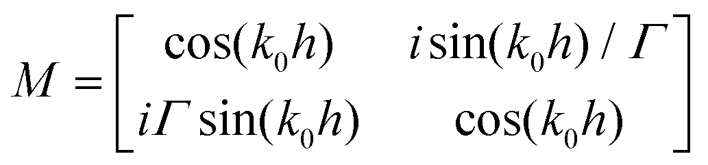 | (1) |
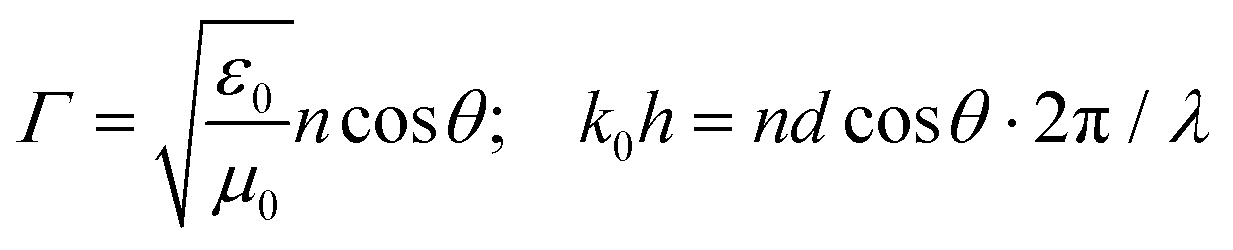 | (2) |
θ and λ are the refractive angle and the wavelength of the incident light, respectively. n and d are the refractive index and the thickness of the layer, respectively. ε0 and μ0 are the vacuum permittivity and vacuum permeability, respectively. Then the characterized matrix for light transmitting through multilayers can be obtained by
 | (3) |
Then the reflectivity R(λ) can be obtained by
 | (4) |
The quantum efficiency (number of electron–hole pairs generated per incident photon) of the GeSn NM RCE photodetector was simulated to make the photodetector resonant at the desired wavelength using Lumerical three-dimensional FDTD. A plane wave was considered as the incident light. The vertical dimension of each layer is from experimental measurements and perfectly matched layer (PML) boundary conditions were used in the top and bottom of the structure. For the lateral directions, period boundaries were used. A power monitor above the GeSn NM was used to obtain the reflectivity (R) and a power monitor below the DBR was used to obtain the transmission (T). The quantum efficiency of the photodetector can be calculated by η = 1 − T − R.
3. Results and discussion
3.1 Device design and material characterization
Fig. 2(a) shows a schematic of the multilayer configuration of the designed transferable GeSn NM RCE photodetectors on the DBR/Si substrate. In the device, the transferrable single-layer GeSn NM serves as the active light absorption material and interdigitated metal fingers are defined as electrical contacts. Highly reflective DBR, consisting of a-Si and SiO2 alternative layers, serves as the bottom mirror, while the GeSn surface acts as the top reflector. Thus, a vertical cavity to confine light is formed and enhances the light–matter interaction. The optical responsivity of the device will be enhanced significantly under resonance conditions. To achieve the designed high-efficiency photodetector, a high-quality and well-controlled GeSn NM and vertical optical cavity are required.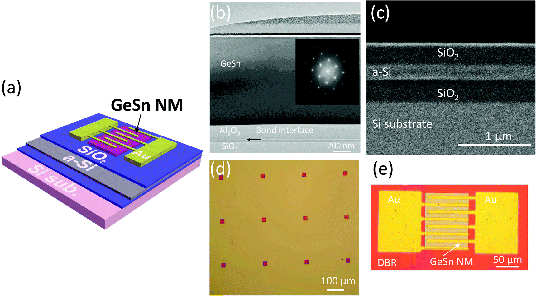 | ||
| Fig. 2 (a) 3D schematic of the designed transferable GeSn NM RCE photodetector. (b) Cross-sectional TEM of the GSOI substrate. The inset is the FFT image of the GeSn layer. (c) Cross-sectional SEM of the DBR with 1.5 pairs of a-Si/SiO2. (d) Optical micrograph of a transferred GeSn NM on a DBR/Si receiver substrate, showing the etchant access holes and smooth NM surface. (e) The top view optical microscopy image of a typical GeSn NM RCE photodetector. | ||
The material quality of the GeSn NM is critical for achieving high-performance NM-based devices. To obtain a high-quality GeSn NM as well as introduce a sacrificial layer, the GSOI substrate serves as the donor wafer for the GeSn NM instead of the as-grown GeSn/Ge/Si. Compared with the as-grown GeSn/Ge/Si substrate, the GSOI as the donor substrate has two advantages: (1) the defective region near the GeSn/Ge or Ge/Si interface in the as-grown GeSn/Ge/Si wafer is removed in the GSOI substrate, resulting in a better NM quality; (2) the oxide layers under the GeSn layer can act as the sacrificial layer which can be easily removed without damaging the GeSn layer. Fig. 2(b) shows the cross-sectional TEM of the developed GSOI substrate, revealing clear interfaces between different layers. Only minor defects are observed in the GeSn layer, indicating the high quality of the GeSn layer. The fast Fourier transform (FFT) pattern of the GeSn layer confirms that the GeSn alloys are single crystalline (inset of Fig. 2(b)).
Next, in order to enable strong light–matter interaction in the GeSn NM through resonance, a highly reflective predesigned substrate without absorption loss is the key. Normally, the DBR to achieve high reflectivity in optoelectronic devices, such as vertical-cavity surface-emitting lasers (VCSELs) or RCE photodetectors, is epitaxially grown with alternate semiconductor layers.24,25 For group-IV devices, strain-balanced GeSn(Si) layers with a wider bandgap might be the material for semiconductor DBR. However, the refractive index contrast of the GeSn(Si) system is low,26 resulting in complex multi-layer growth and a narrow stopband of the DBR. Therefore, we chose the a-Si/SiO2 dielectric DBR and NM transfer instead of semiconductor epitaxy to overcome these issues. Fig. 2(c) shows the cross-sectional SEM image of the DBR/Si receiver substrate with 1.5 pairs of a-Si/SiO2 layers. The DBR consists of alternative a-Si and SiO2 layers with thicknesses of 185 nm/310 nm, respectively. The growth temperature of a-Si and SiO2 is 200 °C so the DBR is compatible with flexible substrates and can be used to extend the design to flexible NM-based optoelectronic devices as well.
Once the donor substrate and receiver substrate were ready, the GeSn NM was released from the GSOI donor substrate and transferred onto the highly reflective DBR/Si receiver substrate. Fig. 2(d) shows an optical micrograph of a transferred GeSn NM on the DBR/Si substrate, showing the etchant access holes, smooth and bubble-free NM. The etchant access holes have a dimension of 20 μm and a pitch of 200 μm. Finally, transferred GeSn NMs were fabricated into photodetector arrays by the processes described in the Experimental section. Fig. 2(e) illustrates an optical microscopy image of one representative fabricated GeSn NM RCE photodetector with a well-defined GeSn NM.
To measure the Sn concentration of the GeSn alloy, SIMS was performed on the as-grown GeSn/Ge/Si substrate, and it confirmed that the Sn concentration of the GeSn alloys is ∼10%. With such a high Sn concentration, the absorption coefficient of GeSn is extended beyond 2 μm and is higher than 6700 cm−1 at 2 μm wavelength. The refractive index of GeSn ranges from 4.30 to 4.36 with different wavelengths. Besides, the strain in the transferred GeSn NM was investigated by Raman spectroscopy. Fig. 3(c) illustrates the measured Ge–Ge longitudinal optical photon peak position of the GeSn NM, as-grown GeSn and Ge bulk. The Ge–Ge mode is at 301.0 cm−1 in the Ge bulk, and shifts to 294.3 cm−1 in the as-grown GeSn due to the introduced Sn, and to 291.9 cm−1 in the GeSn NM. The strain in the GeSn NM can be extracted based on the equation below:27
 | (5) |
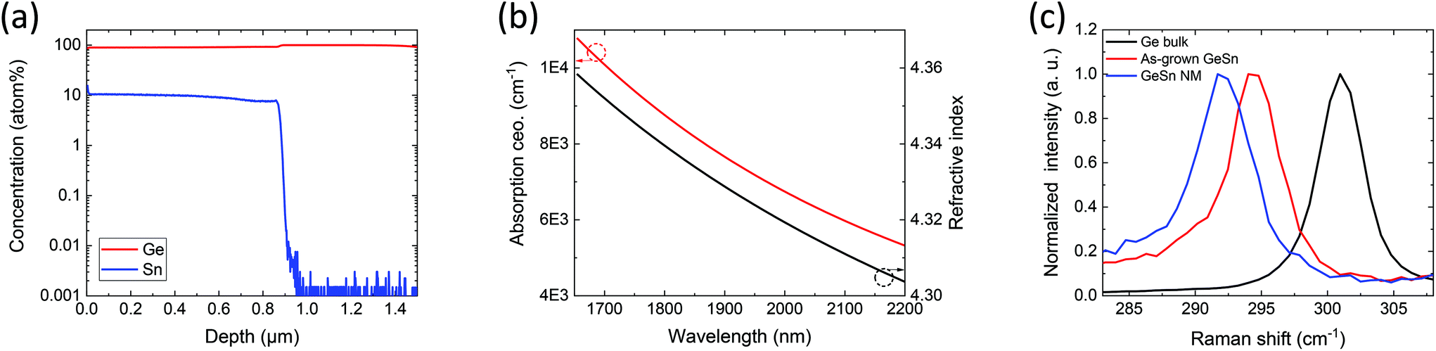 | ||
| Fig. 3 (a) The SIMS profile (Ge and Sn atoms) of the as-grown GeSn/Ge/Si substrate. (b) Optical constants (absorption coefficient and refractive index) of GeSn measured by spectral ellipsometry. (c) Raman spectrum of the GeSn NM compared to those of as-grown GeSn and Ge bulk. | ||
Fig. 4(a) shows the measured normal incidence reflectivity of the DBR with different a-Si/SiO2 pairs (N). The reflectivity of the DBR increases with the a-Si/SiO2 pairs N. With N = 3, the reflectivity at 2 μm wavelength is 97% with a stopband as wide as 600 nm, which covers all the wavelengths of interest attributed to the high contrast of refractive index between a-Si and SiO2. The reflectivity spectra were further verified by a simulation using the transfer matrix method, as indicated by the dashed lines. In contrast to metal mirrors, there is no absorption loss in the DBR. To prove that the DBR has no absorption loss, the optical constants of a-Si and SiO2 were measured and are shown in Fig. 4(b) and (c). a-Si and SiO2 are transparent in the wavelength range of interest and the refractive index contrast between them is as high as 1.1. In the design of the GeSn NM RCE photodetectors, a DBR with 1.5 pairs of a-Si/SiO2 is utilized to obtain a broadband optical response. The measured reflectivity of the DBR (N = 1.5) in free space is 50% (black solid line in Fig. 4(a)). The reflectivity of the DBR (N = 1.5) in the device increases to 82% as estimated by the transfer matrix method (blue dashed line in Fig. 4(a)), which is high enough to demonstrate a strong resonance effect. The reason that the reflectivity of DBR in the device is higher than that of DBR in free space is that the first layer of DBR in the device is SiO2 (n = 1.5) and its refractive index in contrast to the incident media GeSn (n > 4.3) is high. For the free-space DBR, the incident media is air (n = 1) which has a low refractive index in contrast to the first layer (SiO2) of the DBR.
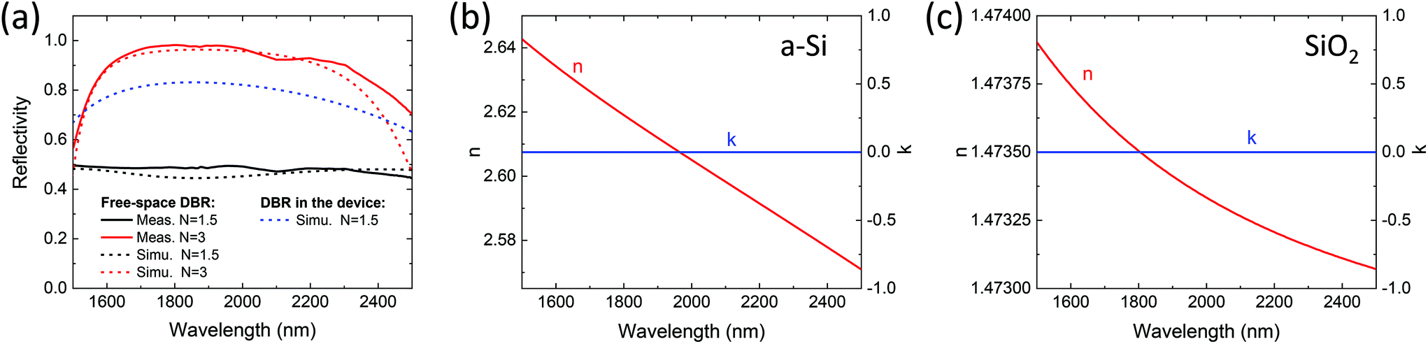 | ||
| Fig. 4 (a) Measured and simulated reflectivity of DBR with different pairs of a-Si/SiO2. Refractive index, n and extinction coefficient, k of (b) a-Si, and (c) SiO2 measured by spectral ellipsometry. | ||
3.2 Performances of transferable GeSn nanomembrane resonant-cavity-enhanced photodetectors
For the transferable GeSn NM RCE photodetector, the dark and photo current–voltage (I–V) curves at room temperature were measured first. As shown in the inset of Fig. 5(a), the light illuminates onto the device normally from a single-mode silica fiber and the current is collected by the electrical probes. We achieved an ohmic contact for the photodetector without any annealing treatment by utilizing Ti/Au as electrodes, as indicated by the linear dark I–V relationship in Fig. 5(a). The possible reason that causes the ohmic contact is that the Fermi-level pinning lowers the hole Schottky barrier height and the unintentional background p-type doping of GeSn during low-temperature growth. The current increases when the device is illuminated by light, demonstrating photodetection ability for the 2 μm wavelength. Fig. 5(b) shows the time-dependent photo-response of the photodetector illuminated by a 2 μm wavelength laser which is periodically turned on and off with a duration of 5 s and a time resolution of 83 ms. During the given cycles, the photodetector responds well to the laser pulse, demonstrating good stability.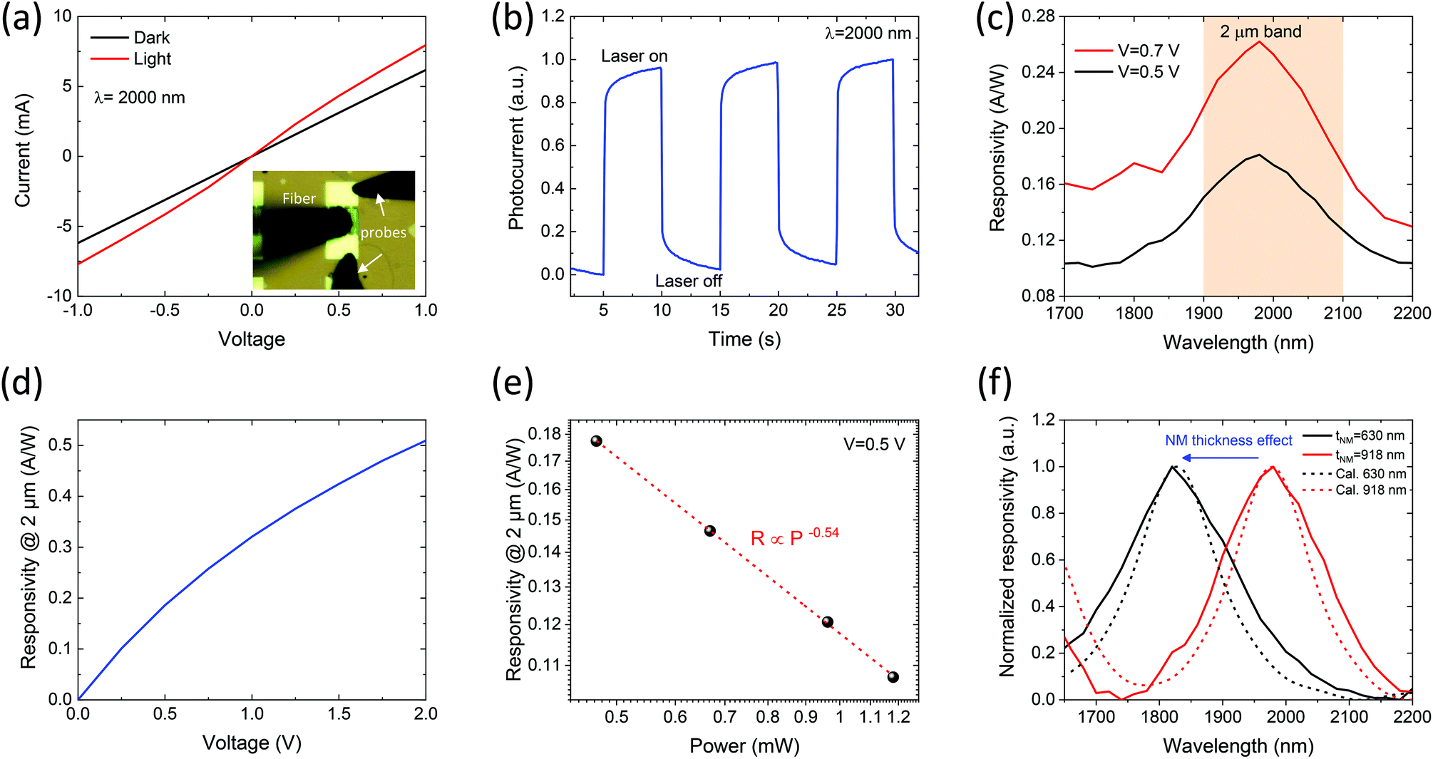 | ||
| Fig. 5 (a) Photo and dark I–V curves of the device. The inset is the measurement configuration of the device. (b) Dynamic photo response behaviors of the photodetector under a laser pulse. (c) Responsivity spectra of the GeSn NM RCE photodetector under bias voltages of 0.5 and 0.7 V. (d) Responsivity versus bias voltage of the photodetector. (e) Excitation-laser-power-dependent responsivity of the photodetector at 2 μm wavelength. (f) Normalized responsivity spectra of the photodetector with different GeSn NM thicknesses (solid lines) and corresponding simulation results (dashed lines). | ||
The RCE effect which enables responsivity enhancement and wavelength tunability is one of the most unique characteristics of the designed photodetectors. To investigate the RCE effect, the responsivity spectra of the RCE GeSn NM photodetector at voltages of 0.5 and 0.7 V were extracted (Fig. 5(c)). Different from the conventional GeSn photodetector whose responsivity decreases gradually with increased wavelength,20,28 the responsivity spectrum of the RCE GeSn NM photodetector demonstrates a distinct peak that is tuned by the structure design rather than the GeSn absorption coefficient. The resonant peak position is at 1980 nm with a wide wavelength range of 350 nm, which covers the whole 2 μm communication band. The responsivity can be further enhanced by increasing DBR pairs, but the wavelength range will be narrow. There is a tradeoff between the responsivity value and the spectral responsivity range, which can be tuned accordingly based on different applications. Moreover, the spectral responsivity can be improved by increasing the bias voltage. The higher bias voltage provides a stronger electric field in the photodetector, resulting in higher carrier collection efficiency. A responsivity of 0.51 A W−1 at 2 μm wavelength is observed under a 2 V bias voltage at room temperature as shown in Fig. 5(d). The responsivity increases linearly in the voltage range of 0 to 1 V and no saturation is observed within 2 V.
The dependence of the responsivity on the excitation laser power at 2 μm wavelength is shown in Fig. 5(e). The responsivity of the photodetector increases as the excitation laser power decreases, indicating that the photodetector is more sensitive to weak light. By fitting the experimental data using a simple power-law dependence, R = APn, a factor n of −0.54 is deduced. The increased responsivity at low excitation power suggests the existence of the localized states either inside GeSn NMs or at the GeSn NM/SiO2 interface. The localized states could trap one type of carrier and prolong the lifetime of the other type of carrier. At a high excitation laser power, the number of the localized states is limited compared to the photogenerated carriers so that the localization effect is not obvious, and the responsivity decreases due to the decreased carrier lifetime.
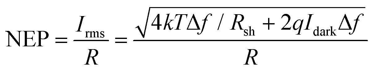
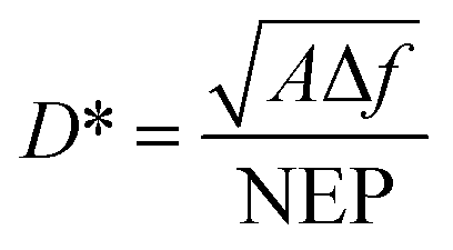
The noise-equivalent power (NEP) and specific detectivity (D*) of the photodetector are calculated based on the equations below:29
 | (6) |
 | (7) |
In addition to enhancing the responsivity value by increasing the bias voltage, the responsivity spectrum of the device can be tuned by the thickness of the GeSn NM due to the dimensional constraint of light, providing a potential application in multi-spectral sensing. To demonstrate the spectral tunability of the device, GeSn NM RCE photodetectors with a thinner NM thickness of 630 nm were fabricated. Fig. 5(f) shows the measured (solid lines) and simulated (dashed lines) normalized responsivity spectra of photodetectors with NM thicknesses of 630 nm and 918 nm. The spectral tunability of RCE GeSn NM photodetectors is observed clearly. As the GeSn NM thickness decreases, the resonant responsivity peak blue shifts by 155 nm. The experimental responsivity spectra match the simulated responsivity spectra well, as shown in the dashed lines in Fig. 5(f), proving that well-controlled spectral tunability of the photodetector and a high-efficiency multi-spectral GeSn NM photodetector array can be achieved on the same substrate by the multiple-step NM transfer, which has the potential for multi-spectral SWIR sensing applications (ESI Fig. S1†).
To figure out and verify the origin of the peak in responsivity peaks in Fig. 5(c), the FDTD simulation was performed. Fig. 6(a) illustrates the simulated quantum efficiency (i.e., number of electron–hole pairs generated by each incident photon) of the GeSn NM RCE photodetector as well as a reference GeSn NM photodetector without cavities. The dimensional structure of the fabricated device is used for the simulation of the RCE GeSn NM photodetector. The non-cavity structure of GeSn/Ge/Si with the same GeSn thickness was simulated for reference. The simulated quantum efficiency spectrum of the RCE GeSn NM photodetector shows a distinct single peak at 1985 nm wavelength which matches the measured peak in the responsivity spectrum, which is from the 4th order Fabry–Perot resonance. The quantum efficiency at resonance is as high as 84% and it is only 29% for the reference GeSn NM without a cavity. Increasing the a-Si/SiO2 pairs of the DBR would make the GeSn NM close to a perfect absorber. Fig. 6(b) shows the optical field profile (squared magnitude of the electric field) of the photodetector under resonance conditions. The incident light is confined in the Fabry–Perot cavity and a standing wave is formed in the cavity, resulting in a strong spatial overlap between the GeSn NM absorber and the optical field.
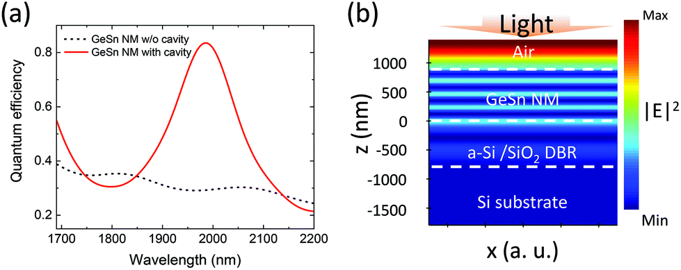 | ||
| Fig. 6 (a) Simulated quantum efficiency spectra of the designed GeSn NM photodetector with and without a cavity. (b) Simulated optical field distribution in the device under resonance conditions. | ||
Finally, to evaluate the potential of the transferable GeSn NM RCE photodetectors, the responsivity of our device is compared to that of the reported GeSn photodetectors. Remarkably, as shown in the responsivity benchmark shown in Fig. 7, the responsivity of this work (0.51 A W−1) is enhanced significantly by more than two orders of magnitude compared to previously reported results of transferable GeSn nanostructured photodetectors (0.001–0.002 A W−1). The enhanced responsivity is attributed to the resonant cavity effect as confirmed by the resonant peaks in the responsivity spectrum and optical simulations. Besides, the enhancement might also be related to the improved GeSn NM quality since it is released from a high-quality GSOI donor substrate where the defective region near interfaces is removed, resulting in a lower trap density and a higher carrier collection efficiency. Even compared with other reported GeSn photodetectors fixed on bulk substrates, the responsivity of our device is among the highest values while the Sn concentration and thickness of our GeSn NM are at a moderate level. This means that transferable GeSn photodetectors without sacrificing the performance or even with better performance can be achieved by GeSn NM. The results propose that integrating the GeSn NM with a cavity is an effective approach for enhancing the light–matter interaction of GeSn-NM-based active optoelectronic devices. Besides, further device optimization, such as increasing the quality factor of the cavity (increasing pairs of the DBR), utilizing the PIN structure or the ferroelectric polymer gate, could improve the performances of the photodetectors further. Having demonstrated the advantages of the GeSn nanomembrane approach over current GeSn technology, it will be more attractive to heterogeneously integrate GeSn NMs with other NMs, thanks to the transferability of the NMs. By integrating GeSn NMs with different NMs (for example Si, Ge, InP or InGaAs), the photodetectors (arrays) can cover a broadband wavelength from visible to mid-infrared and enable more multifunctional photonic circuits, which can hardly be achieved by conventional direct growth approaches on Si. Considering the resonant-cavity-enhanced optical responsivity, spectral tunability, transferability for heterogeneous integration and device miniaturization, the developed GeSn NM RCE photodetectors are proposed as a promising candidate for efficient photodetection in the SWIR range for various applications, such as next-generation optical communications and multi-spectral SWIR sensing.
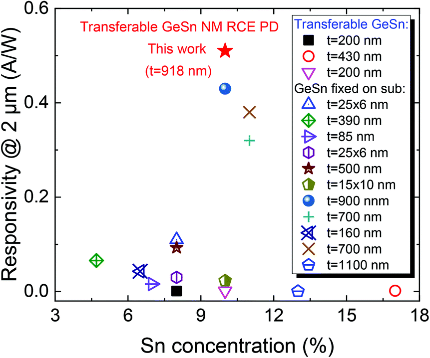 | ||
| Fig. 7 The comparison of responsivity at 2 μm wavelength for the transferable GeSn NM RCE photodetectors and previously reported GeSn-based photodetectors based on different active structures (transferable GeSn19,21,31 and GeSn thin film fixed on bulk substrates18,20,32–38). | ||
4 Conclusions
In conclusion, we have designed, demonstrated and analyzed a novel device, the transferable GeSn NM RCE photodetector, for the first time. The GeSn NM RCE photodetector resonating at 2 μm is designed by FDTD simulations and realized by GeSn alloy epitaxial growth, NM release from the GSOI donor substrate, NM transfer onto a highly reflective DBR/Si substrate and metallization. Due to the integrated resonant cavity and high-quality GeSn NM, a responsivity peak is observed at ∼2 μm wavelength and the value is as high as 0.51 A W−1 at room temperature, which is more than two orders of magnitude higher than the reported values of the transferable GeSn nanostructured photodetectors without resonant cavities. Spectral tunability of the device by NM thickness is demonstrated as well, which is promising for the application of multispectral SWIR sensing. Our approach can be applied to other GeSn-NM-based active devices, such as electro-absorption modulators or light emitters and present a new route towards heterogeneous integrated group-IV photonics with miniaturized devices for various applications.Conflicts of interest
There are no conflicts to declare.Acknowledgements
This work was supported by the National Research Foundation Singapore (NRF-CRP19-2017-01), the Ministry of Education AcRF Tier 2 (T2EP50121-0001 (MOE-000180-01)) and the Ministry of Education AcRF Tier 1 (2021-T1-002-031 (RG112/21)). The authors thank the Nanyang NanoFabrication Centre (N2FC) for assistance in the semiconductor process.Notes and references
- J. Rogers, M. Lagally and R. Nuzzo, Nature, 2011, 477, 45–53 CrossRef CAS PubMed.
- A. Carlson, A. M. Bowen, Y. Huang, R. G. Nuzzo and J. A. Rogers, Adv. Mater., 2012, 24, 5284–5318 CrossRef CAS PubMed.
- J.-H. Seo, K. Zhang, M. Kim, D. Zhao, H. Yang, W. Zhou and Z. Ma, Adv. Opt. Mater., 2016, 4, 120–125 CrossRef CAS.
- C. Xu, R. Pan, Q. Guo, X. Wu, G. Li, G. Huang, Z. An, X. Li and Y. Mei, Adv. Opt. Mater., 2019, 7, 1900823 CrossRef CAS.
- H. Durmaz, P. Sookchoo, X. Cui, R. Jacobson, D. E. Savage, M. G. Lagally and R. Paiella, ACS Photonics, 2016, 3, 1978–1985 CrossRef CAS.
- H.-C. Yuan, J. Shin, G. Qin, L. Sun, P. Bhattacharya, M. G. Lagally, G. K. Celler and Z. Ma, Appl. Phys. Lett., 2009, 94, 013102 CrossRef.
- Z. Xia, H. Song, M. Kim, M. Zhou, T.-H. Chang, D. Liu, X. Yin, K. Xiong, H. Mi and X. Wang, et al. , Sci. Adv., 2017, 3, e1602783 CrossRef PubMed.
- M. Kim, J.-H. Seo, Z. Yu, W. Zhou and Z. Ma, Appl. Phys. Lett., 2016, 109, 051105 CrossRef.
- D.-S. Um, Y. Lee, S. Lim, J. Park, W.-C. Yen, Y.-L. Chueh, H.-j. Kim and H. Ko, ACS Appl. Mater. Interfaces, 2016, 8, 26105–26111 CrossRef CAS PubMed.
- L. Li, H. Lin, Y. Huang, R.-J. Shiue, A. Yadav, J. Li, J. Michon, D. Englund, K. Richardson and T. Gu, et al. , Optica, 2018, 5, 44–51 CrossRef.
- W. Yang, H. Yang, G. Qin, Z. Ma, J. Berggren, M. Hammar, R. Soref and W. Zhou, Appl. Phys. Lett., 2010, 96, 121107 CrossRef.
- R. Soref, Nat. Photonics, 2015, 9, 358–359 CrossRef CAS.
- D. J. Richardson, Science, 2010, 330, 327–328 CrossRef CAS PubMed.
- J. Meyer, Am. J. Nurs., 1986, 86, 976 Search PubMed.
- R. E. Bird and R. L. Hulstrom, Sol. Cells, 1983, 8, 85–95 CrossRef.
- L. S. Rothman, D. Jacquemart, A. Barbe, D. C. Benner, M. Birk, L. Brown, M. Carleer, C. Chackerian Jr., K. Chance and L. e. a. Coudert, et al. , J. Quant. Spectrosc. Radiat. Transfer, 2005, 96, 139–204 CrossRef CAS.
- J. Michel, J. Liu and L. C. Kimerling, Nat. Photonics, 2010, 4, 527–534 CrossRef CAS.
- Q. Chen, S. Wu, L. Zhang, D. Burt, H. Zhou, D. Nam, W. Fan and C. S. Tan, Opt. Lett., 2021, 46, 3809–3812 CrossRef CAS PubMed.
- M. R. Atalla, S. Assali, A. Attiaoui, C. Lemieux-Leduc, A. Kumar, S. Abdi and O. Moutanabbir, Adv. Funct. Mater., 2021, 31, 2006329 CrossRef CAS.
- H. Tran, T. Pham, J. Margetis, Y. Zhou, W. Dou, P. C. Grant, J. M. Grant, S. Al-Kabi, G. Sun and R. A. Soref, et al. , ACS Photonics, 2019, 6, 2807–2815 CrossRef CAS.
- S. An, S. Wu, C. S. Tan, G.-E. Chang, X. Gong and M. Kim, J. Mater. Chem. C, 2020, 8, 13557–13562 RSC.
- L. Zhang, Q. Chen, S. Wu, B. Son, K. H. Lee, G. Y. Chong and C. S. Tan, ECS Trans., 2020, 98, 91 CrossRef CAS.
- E. Hecht and A. Zajac, Addison-Wesley Series in Physics, Addison-Wesley, Reading, Mass, 2003, vol. 23, p. 50 Search PubMed.
- F. Koyama, J. Lightwave Technol., 2006, 24, 4502–4513 CrossRef CAS.
- M. S. Ünlü and S. Strite, J. Appl. Phys., 1995, 78, 607–639 CrossRef.
- H. Tran, W. Du, S. A. Ghetmiri, A. Mosleh, G. Sun, R. A. Soref, J. Margetis, J. Tolle, B. Li and H. A. Naseem, et al. , J. Appl. Phys., 2016, 119, 103106 CrossRef.
- J.-H. Fournier-Lupien, S. Mukherjee, S. Wirths, E. Pippel, N. Hayazawa, G. Mussler, J. Hartmann, P. Desjardins, D. Buca and O. Moutanabbir, Appl. Phys. Lett., 2013, 103, 263103 CrossRef.
- S. Ghosh, K.-C. Lin, C.-H. Tsai, H. Kumar, Q. Chen, L. Zhang, B. Son, C. S. Tan, M. Kim and B. Mukhopadhyay, et al. , Micromachines, 2020, 11, 795 CrossRef PubMed.
- H. Kumar and A. K. Pandey, IEEE Trans. NanoBiosci., 2021, 21, 175–183 Search PubMed.
- B. R. Conley, J. Margetis, W. Du, H. Tran, A. Mosleh, S. A. Ghetmiri, J. Tolle, G. Sun, R. Soref and B. Li, et al. , Appl. Phys. Lett., 2014, 105, 221117 CrossRef.
- Y. Yang, X. Wang, C. Wang, Y. Song, M. Zhang, Z. Xue, S. Wang, Z. Zhu, G. Liu and P. Li, et al. , Nano Lett., 2020, 20, 3872–3879 CrossRef CAS PubMed.
- H. Cong, C. Xue, J. Zheng, F. Yang, K. Yu, Z. Liu, X. Zhang, B. Cheng and Q. Wang, IEEE Photonics J., 2016, 8, 1–6 Search PubMed.
- Y. Dong, W. Wang, S. Xu, D. Lei, X. Gong, X. Guo, H. Wang, S.-Y. Lee, W.-K. Loke and S.-F. Yoon, et al. , Opt. Express, 2017, 25, 15818–15827 CrossRef CAS PubMed.
- W. Wang, Y. Dong, S.-Y. Lee, W.-K. Loke, D. Lei, S.-F. Yoon, G. Liang, X. Gong and Y.-C. Yeo, Opt. Express, 2017, 25, 18502–18507 CrossRef CAS PubMed.
- H. Tran, T. Pham, W. Du, Y. Zhang, P. C. Grant, J. M. Grant, G. Sun, R. A. Soref, J. Margetis and J. Tolle, et al. , J. Appl. Phys., 2018, 124, 013101 CrossRef.
- S. Xu, Y.-C. Huang, K. H. Lee, W. Wang, Y. Dong, D. Lei, S. Masudy-Panah, C. S. Tan, X. Gong and Y.-C. Yeo, Opt. Express, 2018, 26, 17312–17321 CrossRef CAS PubMed.
- S. Xu, K. Han, Y.-C. Huang, K. H. Lee, Y. Kang, S. Masudy-Panah, Y. Wu, D. Lei, Y. Zhao and H. Wang, et al. , Opt. Express, 2019, 27, 26924–26939 CrossRef CAS PubMed.
- C.-H. Tsai, B.-J. Huang, R. A. Soref, G. Sun, H. Cheng and G.-E. Chang, Opt. Lett., 2020, 45, 1463–1466 CrossRef PubMed.
Footnote |
| † Electronic supplementary information (ESI) available. See DOI: https://doi.org/10.1039/d1nr07293e |
| This journal is © The Royal Society of Chemistry 2022 |