
Polarization-based colour tuning of mixed colloidal quantum-dot thin films using direct patterning†
Eva
De Leo
 a,
Aurelio A.
Rossinelli
a,
Patricia
Marqués-Gallego
a,
Lisa V.
Poulikakos‡
a,
David J.
Norris
a and
Ferry
Prins
*ab
a,
Aurelio A.
Rossinelli
a,
Patricia
Marqués-Gallego
a,
Lisa V.
Poulikakos‡
a,
David J.
Norris
a and
Ferry
Prins
*ab
aOptical Materials Engineering Laboratory, ETH Zürich, Leonhardstrasse 21, Zürich 8092, Switzerland. E-mail: ferry.prins@uam.es
bCondensed Matter Physics Center (IFIMAC), Universidad Autónoma de Madrid, Calle Francisco Tomas y Valiente 6, Madrid 29049, Spain
First published on 16th March 2022
Abstract
Colloidal quantum-dots (cQDs) are finding increasingly widespread application in photonics and optoelectronics, providing high brightness and record-wide colour gamuts. However, the external quantum efficiencies in thin-film device architectures are still limited due to losses into waveguide modes and different strategies are being explored to promote the outcoupling of emission. Here we use a template-stripping-based direct-patterning strategy to fabricate linear gratings at the surface of cQD thin films. The linear gratings enhance optical outcoupling through Bragg scattering, yielding bright emission with a strong degree of linear polarization. By patterning linear gratings with different periodicities and orientations onto a film of mixed-colour cQDs, we demonstrate polarization-based active colour tuning of the thin-film emission.
 Ferry Prins | Dr Ferry Prins obtained a Masters in Chemistry from Leiden University (2007) and a PhD in Physics from Delft University of Technology (2011). After postdoctoral stays at MIT and ETH Zürich, he joined the Condensed Matter Physics Center at the Universidad Autónoma de Madrid as a tenure track group leader in 2017, where he now directs the Photonic Nanomaterials and Devices Lab. His group studies the optoelectronic properties of semiconductor nanomaterials, exploring new photonic strategies to control light–matter interactions and developing new techniques to directly visualize energy transport in these materials. |
Introduction
Colloidal quantum dots (cQDs) are highly versatile building blocks for photonic and optoelectronic applications.1 They benefit from solution processability, size-tunable optical bandgaps, high colour-purity, and bright emission. In recent years, a large number of commercial display and lighting technologies using cQDs as the active layer have emerged.2 Such technologies can make optimal use of the size-tunable character of the optical bandgap, providing fine tuning of the emission colour as well as the ability to generate RGB-based white light emission from mixed-colour cQD thin-films.3 Moreover, thanks to the narrow emission spectra as compared to organic emitters, cQD based displays allow for the definition of wider colour gamuts.4–6The high quality modern cQDs yield high internal quantum efficiencies for light emitting devices. However, the outcoupling efficiencies of the emission are generally much lower due to optical losses in the device structure. These optical losses are mainly due to total internal reflection of the emitted light. Specifically, a large portion of the emission gets trapped into waveguide modes of the high refractive index cQD layer. For a typical refractive index of a cQD film of around n = 1.8, as much as 80% of the light undergoes total internal reflection at a cQD-air interface. Importantly, the issue of total internal reflection is not limited to cQD thin-films but is general to all solid-state lighting employing high-refractive-index emitter layers. To overcome the losses associated with total internal reflection, a large number of outcoupling strategies have been developed. Most of these employ external optical elements to redirect the emission and avoid interfacial reflections. Examples of external outcoupling strategies include, for example, microlens arrays7 and scattering films.8 Such external optical elements are particularly useful in combination with LED-based technologies, allowing for the light management to be decoupled from the electronically integrated emitter film.
However, in current implementations of cQD display and lighting technologies, the cQD thin film is most often employed as a backlit down-conversion layer.2,6 In this case, the cQD layer itself is already decoupled from the electronic components of the device. Rather than employing external optical elements for light management, direct patterning of the cQD layer can provide a more straightforward route to create the required surface textures for improved outcoupling. Several direct patterning strategies for cQD thin films have been developed in recent years. Examples include the use of direct lithography onto the film,9–12 using electron-beam or optical lithography techniques. In addition, different printing techniques have shown high-resolution patterning.13,14 Likewise, a number of soft lithography techniques have been employed, using either viscoelastic stamping or moulding of the cQD layer.15–17 Our own group has reported on the patterning of cQD thin films using hard silicon templates.18 This so-called template-stripping technique allows for higher resolution patterning as compared to soft lithography techniques. In past studies, we demonstrated the use of circular Bragg gratings to generate resonant outcoupling of beams of fluorescent emission18 and ring resonators to promote lasing.19
In this work, we expand on these concepts by combining the direct patterning with mixed colloidal quantum-dot thin films to demonstrate polarization-based colour tuning of the outcoupled light. Using linear Bragg gratings, we generate resonant outcoupling of fluorescent emission of the cQDs with a distinct linear polarization state. We present a family of concentric polygonal grating structures (rectangles and hexagons) in which the periodicity of the different axes can be varied, allowing for independent fine-tuning of each axis to match different emission wavelength. Arrays of such concentric polygons allow for the large area integration of linear gratings with different periodicities and orientations into the thin-film of mixed cQDs, enabling polarization-based colour tuning of the thin-film emission.
Results and discussion
We fabricate our patterned thin films using template stripping,18,20 schematically depicted in Fig. 1a. In short, patterned templates are fabricated from silicon wafers using conventional electron-beam lithography and deep-reactive-ion etching. The templates are then coated with an octadecyltrichlorosilane-based self-assembled monolayer to reduce the surface energy of the silicon surface,21 after which colloidal quantum dots are drop-cast onto the template from a 9![[thin space (1/6-em)]](https://www.rsc.org/images/entities/char_2009.gif) :1 hexane/octane (v/v%) dispersion. A glass slide is then attached to the back of the cQD thin film using a UV-curable epoxy. In a final step, the glass/epoxy/cQD stack is mechanically cleaved from the template using a razor blade, exposing the patterned cQD surface. Importantly, the template can be re-used after a simple cleaning step of ultrasonication in chloroform.
:1 hexane/octane (v/v%) dispersion. A glass slide is then attached to the back of the cQD thin film using a UV-curable epoxy. In a final step, the glass/epoxy/cQD stack is mechanically cleaved from the template using a razor blade, exposing the patterned cQD surface. Importantly, the template can be re-used after a simple cleaning step of ultrasonication in chloroform.
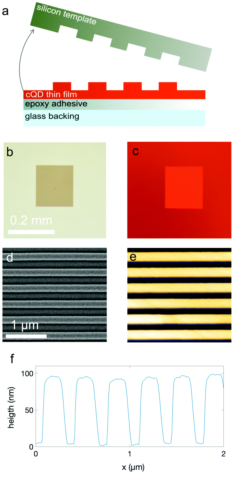 | ||
| Fig. 1 (a) Schematic of template stripping procedure, illustrating the pattern transfer from the hard silicon template to the stripped cQD thin film. (b) Reflectance microscopy image of a linear grating structurewith a periodicity Λ of 350 nm. (c) Fluorescence microscopy image of the same grating structure as in (b). Images in (b) and (c) are taken with a numerical aperture (NA) of 0.06. (d) Scanning Electron Microscope (SEM) image of the same grating structure. (e) Atomic force microscope (AFM) image of the same grating structure. (f) Representative vertical line trace of the AFM image in E, showing an average height of the surface grating of around 90 nm. | ||
Fig. 1b and c show reflectance and fluorescence microscopy images of a linear grating structure patterned onto a red-emitting (λem = 635 nm) CdSe/CdZnS cQD film. The grating structure has 300 lines with a periodicity (or pitch) of 400 nm, demonstrating the large area patterning capability of the template-stripping technique. The high quality of the structure is further emphasized by the scanning electron and atomic force microscopy images shown in Fig. 1d and e, in which no clear defects are observed. An extracted height profile from the atomic force microscopy image is shown in Fig. 1f, showing a height of around 90 nm for the grating profile, consistent with the original etch depth of the template.
The increased brightness of the fluorescence of the grating structure shown in Fig. 1c is a result of increased outcoupling of the emission otherwise trapped in waveguide modes of the thin film.18,22,23 Essentially, the trapping of emission is the result of the momentum mismatch between waveguided light and free-space photons. Bragg gratings efficiently promote outcoupling by providing the waveguided light with additional momentum to couple to free-space photons. The momentum-matching condition is given by the Bragg equation, which governs the angle θ under which waveguided light of a specific wavelength λem is coupled out to free space for a given grating periodicity Λ:
 | (1) |
| λem = Λ·neff. | (2) |
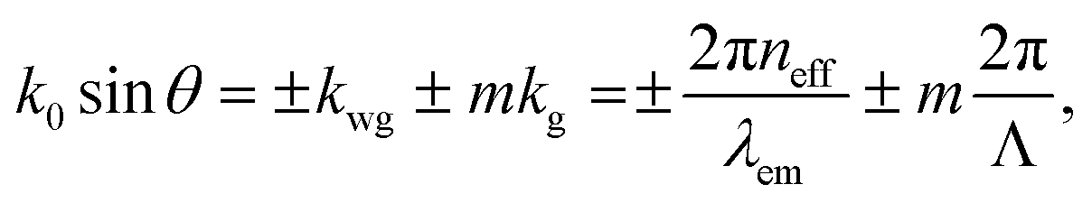
In Fig. 2a we present angle-resolved microscopy images of the fluorescent emission of a series of linear gratings with different periodicities of red-emitting cQD thin films (λem = 635 nm). Angle-resolved images are obtained using k-space microscopy (or back focal–plane imaging) with a high-numerical-aperture objective (NA = 0.7). The bright arcs of emission are consistent with enhanced outcoupling of emission through Bragg scattering from the grating structures. A significant part of the light is coupled out in directions around the surface normal (kx/k0 = ky/k0 = θ = 0) for a grating periodicity of Λ = 400 nm, indicating an effective refractive index of the waveguided mode of neff = 1.58. Along the surface normal direction, the resonant enhancement of the outcoupling is as much as four-fold that of the non-resonant background emission. For longer and shorter periodicities, light is coupled out under shallower angles, consistent with the angular dependence of eqn (1).
 | ||
| Fig. 2 (a) Fluorescence microscopy image of three grating structures with varying periodicities. Image was taken with an NA of 0.06. (b) k-space microscopy image of the three gratings shown in A, showing the angular distribution of outcoupled emission. Angular range of kx/k0 = ±0.7 = ±44°. Intensity is normalized to the maximum intensity among the three images. (c) Angular distribution of the Degree of Linear Polarization (DLP) of the outcoupled emission of the same three grating structures. | ||
Importantly, outcoupling from a linear grating is strongly polarization dependent, as only the waveguided light travelling perpendicular to the grating structure undergoes Bragg scattering.22 To quantify the degree of linear polarization of the outcoupled light, we perform k-space polarimetry.24,25 As can be seen in Fig. 2c, a high degree of linear polarization (DLP) is observed for the resonances. For the grating periodicity of Λ = 400 nm, a DLP of > 0.7 is observed for the surface normal direction (kx/k0 = θ = 0). Our direct patterning strategy therefore allows for spectrally- and polarization-selective outcoupling of emission from a cQD thin-film.
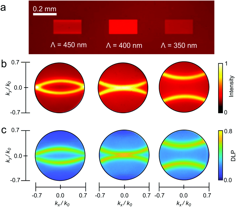
One of the unique advantages of colloidal quantum dot emitters is the ability to create multicolour films using cQDs of different sizes. Combining the size-tunable character of the cQDs with the spectral selectivity of the grating structures, this allows to selectively outcouple different colours from a cQD thin-film. To demonstrate this, we fabricate rectangular concentric grating structures onto a red-green emitting cQD thin-film (λem1 = 540 nm, λem2 = 635 nm). The rectangular concentric grating structure consists of two distinct periodicities (Λ1 = 340 nm, Λ2 = 400 nm) rotated at 90 degrees with respect to each other (see Fig. S1† for an SEM image of the centre of the structure). An image taken with low numerical aperture (NA = 0.06) of the structure is shown in Fig. 3a, illustrating the selective outcoupling of the different colours in the surface normal direction for the different grating structures. For these structures, the outcoupling enhancement in the surface normal direction is less strong than for the pure red coloured film presented in Fig. 2, most likely due to increased absorptive losses in the mixed film. Nevertheless, enhancements of 86% for red emission and 71% for green emission are reached when compared to the non-resonant background emission (see Fig. S3†).
 | ||
| Fig. 3 (a) Fluorescence microscopy image of a concentric rectangular grating patterned onto a red-green emitting cQD thin-film (λem1 = 540 nm, λem2 = 635 nm). The grating consists of two distinct periodicities (Λ1 = 340 nm, Λ2 = 400 nm) rotated at 90 degrees with respect to each other. (b) Fluorescence spectra taken at the center of the structure in A, taken with orthogonal polarizer orientations. (c) Fluorescence microscopy image of an array of the concentric rectangular grating structures shown in A, arranged in the shape of a traffic light figure. (d) Same as (c) with linear polarizer axis aligned along Λ1 (e) Same as (c) and (d), with polarizer aligned along Λ2. All images and spectra taken with NA of 0.06. Scale bars in (d) and (e) correspond to 0.5 mm. | ||
Crucially, the orthogonal orientation of the grating structures allows to associate each colour with a unique linear polarization. In Fig. 3b, we show the polarization-resolved spectrum taken at the centre of the structure with low numerical aperture (NA = 0.06), showing the clear modulation of the spectrum for the different polarizer orientations. For the green emission peak, around 50% intensity modulation is achieved, whereas for the red emission peak this modulation is around 25%. The main limitation for the intensity modulation of each peak is the presence of unpolarized background emission from the thin film.
Despite the limitations in the amplitude of the modulation, significant colour variation can be achieved, as shown in the fluorescence microscopy images presented in Fig. 3c–e. The structures presented here consist of the rectangular gratings of Fig. 3a, arranged in a traffic light figure (see Fig. S2† for a detail of the design of the rectangular array). While the unpolarized image (Fig. 3c) shows yellow-coloured emission of the mixed red and green, high purity of green and red is observed using a polarizer under the respective orientations (see Fig. 3d and e).
Going beyond the two-colour concept, a wider range of colours can be achieved by combining blue, green, and red emitting cQDs (λem1 = 460 nm, λem2 = 540 nm, and λem3 = 620 nm) into a white-light emitting thin film. Using varying periodicities of the linear grating structures allows for a wide tunability of the outcoupled colour, as demonstrated in Fig. 4a. Fig. 4b shows a fluorescence microscopy image of an array of concentric hexagonal grating structures that include the three different periodicities (Λ1 = 275 nm, Λ2 = 340 nm, and Λ3 = 400 nm) that are aligned with the three cQD emission peaks. A schematic of the concentric hexagonal unit cell is shown in Fig. 4c and an SEM image of the centre of the structure is shown in Fig. S1.† The hexagonal arrangement allows for simultaneous resonant outcoupling of white light along the surface normal direction and control over the colour of outcoupled light through the associated linear polarization of each axis of the hexagon. For the hexagonal grating structures, the outcoupling enhancement in the surface normal direction reaches 75% for red emission, 64% for green emission, and 38% for blue emission as compared to the non-resonant background emission (see Fig. S4†). Lower efficiencies for the shorter wavelengths are most likely due to the increased losses in the film at those wavelengths.
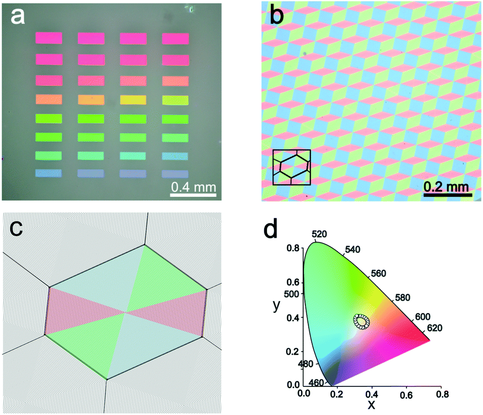 | ||
| Fig. 4 (a) Fluorescence microscopy image of linear gratings of varying periodicities (Λ = 265–420 nm, with 5 nm increments) patterned onto a red-green-blue emitting cQD thin-film (λem1 = 460 nm, λem2 = 540 nm, and λem3 = 620 nm). (b) Fluorescence microscopy image of an array of concentric hexagonal grating structures. The grating consists of three distinct periodicities (Λ1 = 275 nm, Λ2 = 340 nm, and Λ3 = 400 nm) rotated with respect to each other. (c) Schematic of the design of the structure in (b) to illustrate the hexagonal unit cell, corresponding to the black outline in the bottom-left corner of (b). Each hexagon consists of 50 concentric grooves. (d) CIE diagram visualizing the color change generated by the polarization dependence of the emission spectrum of the structure in (b). All images and spectra taken with NA = 0.06. | ||
Using a linear polarizer, the ratios between the different colours of the hexagonal array of Fig. 4b can be modulated, with the resulting spectra at different polarizer orientations shown in Fig. S5.† It is important to note that due to the vectorial nature of the polarization of light, it is not possible to independently control the transmission of the different peaks of the RGB spectrum. Nevertheless, the polarization dependence allows us to generate a tunable RGB white light source that, depending on the polarizer angle, can generate a warmer or cooler tone of white. To illustrate this, we map the spectra of Fig. S5† onto the CIE colour space for each polarizer angle, as shown in Fig. 4d. This demonstration of a tunable white-light source is of particular relevance in the context of cQD based technologies for ambient lighting. Importantly, the polarization-dependent path within the colour space can be further fine-tuned by introducing slight variations in the cQD composition or in the grating periodicities of the concentric hexagon, which would allow to shift the position, orientation, and aspect ratio of the circular path within the CIE colour space.
Conclusions
In conclusion, we have demonstrated that the direct patterning of cQD thin films with linear gratings leads to enhanced outcoupling efficiencies with a strong degree of linear polarization. This structuring strategy is particularly powerful in combination with mixed cQD thin-films in which different colours of emission can be selectively enhanced using grating structures of varying periodicities. Importantly, while we have limited this study to the resonant enhancement of RGB colours, intermediate periodicities can generate a wide spectrum of other colours, as demonstrated in Fig. 4a. Making use of the strong degree of linear polarization of the outcoupled light, we have shown that through the arrangement of linear gratings with different periodicities and orientations we can achieve polarization-based active colour tuning of the emission. Further improvements in the outcoupling efficiencies can potentially be achieved using more elaborate patterning strategies, such as sinusoidal grating structures which present higher diffraction efficiencies.26 This work demonstrates the versatility of direct patterning as an alternative to external light management strategies. Finally, it is worth noting that while sub-micron feature sizes requiring electron-beam lithography are typically considered too costly for widespread use in applications, the reusability of the patterned templates may provide a viable route towards cost-effective large-area fabrication with sub-micron resolution.Methods
Patterned silicon (001) templates of 20 × 20 mm in size were fabricated using standard electron beam lithography in combination with deep-reactive-ion etching. Prior to processing, templates were cleaned using sonication in acetone and isopropanol and pre-baked at 180 °C for 10 min. A 200 nm layer of PMMA (AR-P 672.03 950 K) was deposited onto the Si using two steps of spincoating (6000 rpm, 60 s) and baking (at 180 °C for 5 min). The grating patterns were then written using an electron-beam system (Vistec, EBPG 5200) followed by development for 2 min in MIBK:IPA (1:2 ratio) followed by 1 min in fresh IPA. The pattern was then etched into the Si templates using a deep reactive-ion etching system (Alcatel, AMS-200 I Speeder). The remaining PMMA mask was dissolved in acetone, followed by an isopropanol rinse. After patterning, the templates were cleaned using O2 plasma (600 W, 3 min) and a piranha treatment (1:1 (v/v%) H2O2/H2SO4, 15 min). Critically, to enable efficient stripping of the QDs from the template, an octadecyltrichlorosilane-based self-assembled monolayer was applied using a modified procedure from Lessel et al.21 After surface modification, a water contact-angle of >110° was obtained.
Synthesis of colloidal quantum-dots of CdSe/CdS (blue) and CdSe/CdZnS (red and green) was performed using existing synthetic methods27–30 with modifications described previously in Prins et al.18 To improve film quality, special care was taken to remove any excess ligand after synthesis by performing two cycles of precipitation of the dispersion with methyl acetate, followed by centrifugation and redispersion in hexane. Drop-casting onto the silicon templates was performed using a 9:1 (v/v%) hexane/octane mixture with optical densities (1 cm optical path length) of 2.0 for the red cQDs, using 35 μL for a 20 × 20 mm template. Mixed red-green films were prepared using an optical density ratio of 1:4 with a total optical density of 1.0. For mixed red-green-blue films, this ratio was 1:18:32 for a total optical density of 1.0. The excess of short-wavelength emitters in these mixtures is to compensate for Förster resonance energy transfer within the film, causing the colour balance to shift to the long-wavelength emitters.31 Drop-cast films were stripped from the template by attaching a glass slide to the cQD thin-film using a UV-curable epoxy (Norland 61, 10 min curing) and releasing the cQD/epoxy/glass stack from the template using a razor blade.18
Fluorescence microscopy was performed using an inverted optical microscope (Nikon Ti–U) equipped with a blue emitting LED (Thorlabs, M385PLP1-C5), suitable fluorescent filtering (Semrock, DI02-R405) and a CCD camera (EuroMex, CMEX DC.5000-C). Emission spectra were recorded using a spectrograph and an EMCCD camera (Princeton Instruments, SpectraPro HRS-300, ProEM HS 1024BX3) with a 300 g mm−1 grating with a blaze of 500 nm. Angle-resolved k-space measurements were performed by placing a Fourier-transforming lens (Thorlabs, AC254-080-A-ML) at one focal length away from the microscope exit-port focal plane. Polarization-resolved images and spectra were recorded using a rotatable linear polarizer (Thorlabs, WP25M-VIS) and optional quarter-wave plate (Thorlabs, AQWP05M-580) introduced directly after the microscope objective using a home-built cage structure (Thorlabs). Images and spectra were collected using a low NA objective with a 2x magnification (Nikon, CFI Plan Achro 2X, NA = 0.06). Angle-resolved k-space measurements were collected using a high NA objective with 60x magnification (Nikon, CFI S Plan Fluor, ELWD 60XC, NA = 0.7).
Author contributions
EDL and FP designed the project with input from DJN. EDL performed device fabrication and characterization. PMG synthesized the materials. AR and LP assisted in the sample preparation. EDL wrote the original draft of the manuscript. FP supervised the project. All authors contributed to the discussion of the results and to the revision of the paper.Conflicts of interest
There are no conflicts to declare.Acknowledgements
This work was supported by the Swiss National Science Foundation under the Ambizione program (PZ00P2_161243). We thank Y. Fedoryshyn, A. Olziersky, U. Drechsler, and M. Sousa for assistance in the fabrication and characterization.References
- F. P. G. de Arquer, D. V. Talapin, V. I. Klimov, Y. Arakawa, M. Bayer and E. H. Sargent, Science, 2021, 373, eaaz8541 CrossRef PubMed.
- A. Nurmikko, Nat. Nanotechnol., 2015, 10, 1001–1004 CrossRef CAS PubMed.
- Y. Shu, X. Lin, H. Qin, Z. Hu, Y. Jin and X. Peng, Angew. Chem., Int. Ed., 2020, 59, 22312–22323 CrossRef CAS PubMed.
- Y. Shirasaki, G. J. Supran, M. G. Bawendi and V. Bulović, Nat. Photonics, 2013, 7, 13–23 CrossRef CAS.
- K. Bourzac, Nature, 2013, 493, 283 CrossRef CAS PubMed.
- Z. Liu, C.-H. Lin, B.-R. Hyun, C.-W. Sher, Z. Lv, B. Luo, F. Jiang, T. Wu, C.-H. Ho, H.-C. Kuo and J.-H. He, Light: Sci. Appl., 2020, 9, 1–23 CrossRef PubMed.
- S. Möller and S. R. Forrest, J. Appl. Phys., 2002, 91, 3324 CrossRef.
- R. Bathelt, D. Buchhauser, C. Gärditz, R. Paetzold and P. Wellmann, Org. Electron., 2007, 8, 293–299 CrossRef.
- T. S. Mentzel, D. D. Wanger, N. Ray, B. J. Walker, D. Strasfeld, M. G. Bawendi and M. A. Kastner, Nano Lett., 2012, 12, 4404–4408 CrossRef CAS PubMed.
- K. Miszta, F. Greullet, S. Marras, M. Prato, A. Toma, M. Arciniegas, L. Manna and R. Krahne, Nano Lett., 2014, 14, 2116–2122 CrossRef CAS PubMed.
- D. B. Dement, M. K. Quan and V. E. Ferry, ACS Appl. Mater. Interfaces, 2019, 11, 14970–14979 CrossRef CAS PubMed.
- C. D. Dieleman, W. Ding, L. Wu, N. Thakur, I. Bespalov, B. Daiber, Y. Ekinci, S. Castellanos and B. Ehrler, Nanoscale, 2020, 12, 11306–11316 RSC.
- V. Wood, M. J. Panzer, J. Chen, M. S. Bradley, J. E. Halpert, M. C. Bawendi and V. Bulović, Adv. Mater., 2009, 21, 2151–2155 CrossRef CAS.
- S. J. P. Kress, P. Richner, S. V. Jayanti, P. Galliker, D. K. Kim, D. Poulikakos and D. J. Norris, Nano Lett., 2014, 14, 5827–5833 CrossRef CAS PubMed.
- L. A. Kim, P. O. Anikeeva, S. A. Coe-Sullivan, J. S. Steckel, M. G. Bawendi and V. Bulović, Nano Lett., 2008, 8, 4513–4517 CrossRef CAS PubMed.
- T. H. Kim, K. S. Cho, E. K. Lee, S. J. Lee, J. Chae, J. W. Kim, D. H. Kim, J. Y. Kwon, G. Amaratunga, S. Y. Lee, B. L. Choi, Y. Kuk, J. M. Kim and K. Kim, Nat. Photonics, 2011, 5, 176–182 CrossRef CAS.
- H. Keum, Y. Jiang, J. K. Park, J. C. Flanagan, M. Shim and S. Kim, ACS Nano, 2018, 12, 10024–10031 CrossRef CAS PubMed.
- F. Prins, D. K. Kim, J. Cui, E. De Leo, L. L. Spiegel, K. M. McPeak and D. J. Norris, Nano Lett., 2017, 17, 1319–1325 CrossRef CAS PubMed.
- B. Le Feber, F. Prins, E. De Leo, F. T. Rabouw and D. J. Norris, Nano Lett., 2018, 18, 1028–1034 CrossRef CAS PubMed.
- P. Nagpal, N. C. Lindquist, S. H. Oh and D. J. Norris, Science, 2009, 325, 594–597 CrossRef CAS PubMed.
- M. Lessel, O. Bäumchen, M. Klos, H. Hähl, R. Fetzer, M. Paulus, R. Seemann and K. Jacobs, Surf. Interface Anal., 2015, 47, 557–564 CrossRef CAS.
- J. M. Lupton, B. J. Matterson, I. D. W. Samuel, M. J. Jory and W. L. Barnes, Appl. Phys. Lett., 2000, 77, 3340–3342 CrossRef CAS.
- J. M. Ziebarth and M. D. McGehee, J. Appl. Phys., 2005, 97, 064502 CrossRef.
- C. I. Osorio, A. Mohtashami and A. F. Koenderink, Sci. Rep., 2015, 5, 1–7 Search PubMed.
- E. De Leo, A. Cocina, P. Tiwari, L. V. Poulikakos, P. Marqués-Gallego, B. Le Feber, D. J. Norris and F. Prins, ACS Nano, 2017, 11, 12167–12173 CrossRef CAS PubMed.
- N. Lassaline, R. Brechbühler, S. J. W. Vonk, K. Ridderbeek, M. Spieser, S. Bisig, B. Le Feber, F. T. Rabouw and D. J. Norris, Nature, 2020, 582, 506–510 CrossRef CAS PubMed.
- W. William Yu, L. Qu, W. Guo and X. Peng, Chem. Mater., 2003, 15, 2854–2860 CrossRef.
- P. Reiss, J. Bleuse and A. Pron, Nano Lett., 2002, 2, 781–784 CrossRef CAS.
- W. K. Bae, K. Char, H. Hur and S. Lee, Chem. Mater., 2008, 20, 531–539 CrossRef CAS.
- K. H. Lee, J. H. Lee, W. S. Song, H. Ko, C. Lee, J. H. Lee and H. Yang, ACS Nano, 2013, 7, 7295–7302 CrossRef CAS PubMed.
- A. Mork, M. Weidman, F. Prins and W. Tisdale, J. Phys. Chem. C, 2014, 118, 13920–13928 CrossRef CAS.
Footnotes |
| † Electronic supplementary information (ESI) available: Details on characterization. See https://doi.org/10.1039/d1nr07136j |
| ‡ Current address: Department of Mechanical and Aerospace Engineering, UC San Diego, 9500 Gilman Drive, La Jolla, California 92093-0411, USA. |
| This journal is © The Royal Society of Chemistry 2022 |