
 Open Access Article
 This Open Access Article is licensed under a Creative Commons Attribution-Non Commercial 3.0 Unported Licence
Effects of nanostructuration on the electrochemical performance of metallic bioelectrodes†
Sahba
Mobini
 *a,
María Ujué
González‡
a,
Olga
Caballero-Calero‡
a,
Erin E.
Patrick
b,
Marisol
Martín-González
a and
José Miguel
García-Martín
a
*a,
María Ujué
González‡
a,
Olga
Caballero-Calero‡
a,
Erin E.
Patrick
b,
Marisol
Martín-González
a and
José Miguel
García-Martín
a
aInstituto de Micro y Nanotecnología, IMN-CNM, CSIC (CEI UAM+CSIC), Isaac Newton 8, E-28760, Tres Cantos, Madrid, Spain. E-mail: sahba.mobini@csic.es
bDepartment of Electrical and Computer Engineering, University of Florida, Center Drive 968, Gainesville, FL 32603, USA
First published on 5th February 2022
Abstract
The use of metallic nanostructures in the fabrication of bioelectrodes (e.g., neural implants) is gaining attention nowadays. Nanostructures provide increased surface area that might benefit the performance of bioelectrodes. However, there is a need for comprehensive studies that assess electrochemical performance of nanostructured surfaces in physiological and relevant working conditions. Here, we introduce a versatile scalable fabrication method based on magnetron sputtering to develop analogous metallic nanocolumnar structures (NCs) and thin films (TFs) from Ti, Au, and Pt. We show that NCs contribute significantly to reduce the impedance of metallic surfaces. Charge storage capacity of Pt NCs is remarkably higher than that of Pt TFs and that of the other metals in both morphologies. Circuit simulations of the electrode/electrolyte interface show that the signal delivered in voltage-controlled systems is less filtered when nanocolumns are used. In a current-controlled system, simulation shows that NCs provide safer stimulation conditions compared to TFs. We have assessed the durability of NCs and TFs for potential use in vivo by reactive accelerated aging test, mimicking one-year in vivo implantation. Although each metal/morphology reveals a unique response to aging, NCs show overall more stable electrochemical properties compared to TFs in spite of their porous structure.
Introduction
There is a growing body of research on the use of electricity in interaction with biological systems for therapeutic, diagnostic, and research purposes. Implantable devices (in vivo) such as neural interfaces for recording and stimulation,1 spinal cord stimulators for chronic pain treatment, and low voltage stimulators for accelerated healing of skin ulcers and non-union bone fractures2,3 are used in several clinical trials and some of them are approved by health and safety agencies. In addition, devices for in vitro electrical stimulation and recording are being increasingly studied due to their numerous prospective applications as screening and research tools. Such in vitro devices include, but are not limited to, devices for measuring the electrical impedance of cells to evaluate specific biological activities (e.g., proliferation),4 devices for inducing specific cell responses by means of low voltage electrical stimulation (e.g., cell migration, differentiation),3,5,6 and devices for stimulating and/or recording electrical activities of cells using multi-electrode arrays (MEAs) and multipurpose setups (e.g., lab-on-a-chip).7–9In both in vivo and in vitro electrical stimulation and recording devices, electrodes are the key components responsible for communicating electrical signals with the extracellular fluid (ECF). For biologically safe and effective stimulation and recording, electrodes should provide several physical, electrochemical, mechanical, and biological properties that might not be found in a single material. The main strategy for developing bioelectrodes that deliver the desirable electrical properties with the required mechanical and biological features is depositing biocompatible conductive materials with superior electrical properties on substrates that provide the required mechanical and biological merits.10 Clearly, the deposited materials should present excellent conductivity to be able to transfer electrons to/from the electrode surface. At the interface of the bioelectrodes and the ECF, charges are transferred through faradaic (i.e., electron injection) and non-faradaic (i.e., capacitive charge injection via the movement of ions within the electrical double layer) mechanisms. faradaic mechanisms give rise to several reversible and irreversible electrochemical reactions. Safe charge transfer links to reversible faradaic reactions (e.g., pseudocapacitive behaviour of Pt) and capacitive charge injection.11 The favourable characteristics of bioelectrodes are mainly quantified by: (1) large capacitance of the double layer (Cdl) that corresponds with low signal distortion and attenuation; (2) low electrical impedance (Z) that reduces thermal noises and attenuation at the external amplifier in recording scenarios; (3) high charge storage capacity (CSC) that reflects the sum of charges passing to the electrolyte within the voltage window of water electrolysis.12
Currently common materials used to fabricate bioelectrodes are biocompatible metals and their derivatives (e.g., gold,13 platinum,14 titanium nitride,15 and iridium oxide16), conductive polymers and composites (e.g., PEDOT17), and carbon derivatives.18,19 Among metals, gold and platinum are frequently used in the fabrication of the bioelectrodes, in particular as neural stimulators and recording devices in vitro and in vivo. Titanium has also been tested as bioelectrode in vitro20 and in vivo,21 but not as broadly as those noble metals, mainly due to fast oxidation of the surface that increases the risk of changes in electrical properties. However, the possible use of Ti in fabrication of bioelectrodes has been always motivating, due to its extensive commercial application as dental and bone implants, which could possibly serve as coinciding electrical stimulator.22 Therefore, in this work we focused on Pt, Au, and Ti to cover a comprehensive characterization for a wide range of applications and research interests.
The benefit of using nanostructures and nanoroughness in improving the capacitance of double layer in gold, platinum and iridium oxide electrodes has been studied lately. Nanostructures are advantageous in this application because the electrochemical characteristics are significantly influenced by the total effective surface area exposed to the electrolyte. Nanostructures provide larger effective surface area that explicitly reduces Z and improve safe charge transfer. This is relevant for the development of miniaturized bioelectrodes that are less invasive and able to record and stimulate precisely in small areas down to the single cells. For example, Pt-black (nanostructured platinum) coatings fabricated by means of electrochemical deposition revealed at least four times decrease in Z at 1 kHz and six times increase in charge injection limit (charge storage capacity within maximum operating voltage window) compared to a Pt thin film.23 Gold nanostructures fabricated using deposition of nanoparticles or chemical roughening also showed dramatically reduced Z and enhanced charge injection limit.24 Nevertheless, the performance and application of some of these nanostructures are compromised because of impurities generated during fabrication. For instance, traditional electrochemical roughening methods, which are used to produce Pt-black, introduces lead impurities25 and corrosion roughening of Au generates silver impurities.26 Therefore, physical fabrication methods that offer high purity, such as electron-beam evaporation and sputtering, are preferred. Among the available physical techniques, glancing-angle deposition with magnetron sputtering (GLAD-MS) is one of the trending methods for generating pure metallic nanostructures,27 especially due to the ability to manufacture on a larger scale in a cost-effective manner.28 Previously, such nanostructured surfaces were explored for applications, such as antibacterial orthopedic implants,29 biosensors,30 and solar cells.31 We suggest that this scalable and environmentally friendly fabrication method offers significant advantages for developing high-quality stimulation and recording bioelectrodes.
The electrochemical properties of the bioelectrodes should be analysed in the context of a relevant application condition. For instance, one- and two-electrode setups with current and/or voltage-controlled systems are distinctively used for in vivo and in vitro stimulation/recording and therefore, it is important to assess the behaviour of bioelectrodes within these configurations. Every electrode–electrolyte system affects the amplitude and shape of the applied signal. This is directly related to the capacitance of the double layer and faradaic reactions at the electrode–electrolyte interface.11 The accuracy of the delivered signal can be assessed experimentally by the direct measurement of the signals in the cell culture vessel or tissue, and/or virtually by simulating the electrochemical behaviour of electrodes.
Another consideration is the long-term performance of the bioelectrodes in vivo. At the implantation site, implants are exposed to adverse reactive chemicals such as reactive oxygen species (ROS) produced by immune system cells in response to the surgical procedure of implantation and device materials, and in some cases by a specific disease.32 Therefore, for chronic use, the stability of the electrical performance of the bioelectrodes should be tested in similar conditions.33 To estimate the durability and performance of bioelectrodes in a biological environment, several fast-track mimicry conditionings are used. In particular, accelerated aging in 60 °C PBS and reactive accelerated aging in 80 °C PBS + H2O2 have been previously tested, and the latter is approved by the Food and Drug Administration (FDA) for predicting the life-time of neural implants.34
In this study, we focused on Au, Pt, and Ti for their use as bioelectrodes for possible future applications in vivo and in vitro. We performed a comprehensive characterization of the electrochemical properties of these metals in nanocolumnar and thin film morphology. We used glancing-angle deposition with magnetron sputtering as a versatile fabrication method for developing morphologically similar nanostructured surfaces from Au, Pt and Ti with ultra-high purity. We also simulated the performance of each material/morphology in applying pulse signals and demonstrated the advantages of nanostructures on the improvement of the accuracy in signal delivery. Our study also encompassed testing the durability of nanostructured surfaces and thin films for in vivo application using reactive accelerated aging test. We investigated the effect of aging in the electrochemical properties and material chemistry and morphology.
Experimental
Sample fabrication and preparation
Nanostructured electrodes were fabricated from Ti, Au, and Pt on glass substrates by means of the glancing-angle deposition technique with magnetron sputtering (GLAD-MS).35,36 The schematic of the fabrication method and relevant parameters are depicted in ESI, Fig. S1.† Briefly, glass substrates, 8 mm × 8 mm with ∼0.75 mm thickness (Präzisions Glas & Optik GmbH, Germany), were cleaned and loaded in the ultra-high vacuum chamber (base pressure in the 10–10 mbar range). Argon was used as sputter gas at a pressure of 1.5 × 10⁻³ mbar, the lowest value that allowed stable plasma formation, in order to maximize the ratio between ballistic and thermalized atoms and consequently improve the definition of the nanocolumns.37 Circular targets with diameters of 3.8 cm for Au and Pt, and 5 cm for Ti were used. The distance between substrate and target was dAu = 19 cm, dPt = 19 cm and dTi = 22 cm. The magnetron sources were supplied by AJA International Inc. and included a cylindrical metallic chimney (length L: 4.5 cm for Au and Pt, 9 cm for Ti) placed on top of the target that increased the collimation of the sputtered atomic flux and trapped many of the thermalized atoms.38 Direct current excitation was used by means of an electromagnetic generator set at a constant power of 100 W for Au and Pt, and 300 W for Ti. With these conditions, the visible plasma glow remained more than 10 cm away from the substrate and the deposition took place in the so-called weak plasma regime.39 The substrate was placed in front of the target (i.e., parallel configuration) and subsequently tilted an angle α (αAu = 80°; αPt = 80°; αTi = 75°) in order to achieve the GLAD condition. The inclination angle for the nanocolumns that develop in GLAD-MS, β, depends on atomic-shadowing effects and kinetic-energy induced relaxation processes.39,40 The duration of sputtering was adjusted to obtain nanocolumnar (NCs) structures with thickness of ∼250 nm (tAu = 50 min; tPt = 65 min; tTi = 90 min). Continuous thin films (TF) of Au, Pt and Ti, nominally ∼30 nm thick, were fabricated as control groups in the same setup using the standard configuration, i.e. with the substrate being parallel to the target (α = 0°). An initial bonding layer of Ti (∼2 nm) was deposited first for all samples (NCs and TFs) using the standard parallel configuration to increase the adhesion between the glass substrate and the metallic layer.Morphological characterization and elemental analyses
The microstructure of the electrodes was studied by scanning electron microscopy (SEM), using a Verios 460 field emission microscope (FEI Company, Hillsboro, OR, USA). Images were taken at 2 kV with a beam current of 25 pA. SEM images are used for estimating the surface area ratio between NCs and TFs. Nanocolumns are assumed as perfect tilted cylinders with elliptical cross sections distributed in a periodic array. The average size of nanocolumns and the average distance between two nanocolumns were measured from the SEM images. The surface area of each cylinder is calculated from the estimated NCs height (obtained from cross-sectional images) and the size of ellipses. Finally, the ratio between the surface including nanocolumns (NCs area) and the flat surface (TFs area) is computed. In order to determine the elemental composition of the samples, energy dispersive X-ray spectroscopy (EDX) was performed using an EDX detector (EDAX Octane Plus, Ametek B.V., Tilburg, Netherlands). The spectra were taken with 400 pA beam current and a beam energy ranging from 5 to 15 kV depending on the elements to be detected. Atomic force microscopy (AFM) has been performed using a Dimension Icon microscope (Bruker Corporation, Billerica, MA, USA) operating in non-contact mode and using commercial probes model NT-TP-HRES (NEXT-TIP, Madrid, Spain) with a resonance frequency about 330 kHz, a spring constant about 40 N m−1 and a 2 nm nominal radius. Raman spectroscopy to detect the presence of TiOx was carried out with a LabRam HR confocal microscope (Jobin Yvon, France), using a Nd:YAG laser of 532 nm wavelength. The thickness of the TFs was determined by means of ellipsometry with a spectral ellipsometer M-2000FI (J. A. Woollam Co., Inc., Lincoln, NE, USA). Measurements were performed at angles of 55, 60 and 65 degrees, from 300 to 1600 nm. Results were fitted using CompleteEASE software (J. A. Woollam Co., Inc., Lincoln, NE, USA).Electrochemical characterization
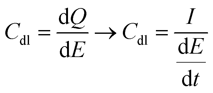
For handling purpose during electrochemical characterizations, a 0.6 mm diameter platinum wire was attached to samples by means of conductive epoxy (EPO-TEK® H20E, Epoxy Technology Inc., USA), and cured at 120° C for 30 min. Then, the connection was sealed using SEM compatible embedding resin (Technovit® 5071, KULZER GmbH, Germany). Before each measurement the quality of the connections was checked and repaired if needed. Electrochemical characterizations were performed using a potentiostat with FRA32 M module (Autolab, Metrohm Hispania) in a three-electrode setup. A platinum mesh (8 mm × 11 mm) was used as a counter electrode and an Ag/AgCl electrode, with 6 mm diameter (RE-1B, Biologic) was used as a reference electrode. A miniaturized chamber was used to fix the electrodes at 10 mm distance inside the electrolyte. 300 μl electrolyte solution of PBS (PBS tablets, EMD Millipore, Germany) was added to the chamber for each assay. This fixed volume was used to accurately control the height of the electrode immersed in the electrolyte (3 mm) (see Fig. S4†). The electrolyte was refreshed for each measurement. Electrical impedance spectroscopy (EIS) is performed in the frequency window of 1 Hz to 100 kHz with a sinusoidal excitation signal of 10 mV. Bode and Nyquist diagrams were analysed in Nova 2.1 software. We repeated the EIS measurement in at least three independent studies. The open circuit potential (OCP) for each measurement was recorded to be reproducible with small standard deviation except for titanium thin film that fluctuates largely, possibly due to the formation of an oxidation layer or the limitation of our measurement system for small OCPs (close to zero). Cyclic Voltammetry (CV) tests have been performed within the water potential window recommended for Pt [−0.5 V, +0.8 V] with sweep rate of 0.1 V s−1. The integral of the cathodic part of the CV diagram (first cycle) is estimated by Origin software (OriginLab Corporation, Northampton, MA, USA) and used for calculation of CSC, eqn (1), where I is current intensity, V is potential, ν is the sweep rate and A is the geometric area of the electrode exposed to electrolyte.41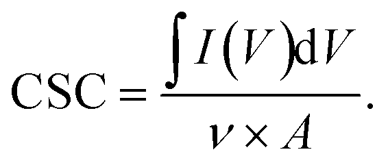 | (1) |
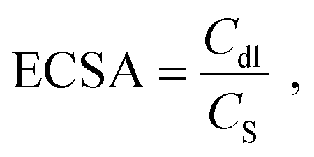
In order to experimentally obtain the electrochemically active surface area (ECSA), we used eqn (2):42,43
 | (2) |
 | (3) |
Simulation
Evaluating the pulse response of the electrode materials is another useful tool to assess how well suited they are for stimulation applications.11 To do this, one must fit the impedance spectrum to an equivalent circuit. In the present cases, the data were fit to an equivalent circuit matching the model for a blocking (i.e., non-reactive) system, which can be represented by a constant phase element (CPE) in parallel with a resistor (Rf), together in series with the electrolyte resistance (Re), the so-called Randles circuit. The CPE is an element whose impedance is given by eqn (4) where ω is the angular frequency, and α (a constant between 0 and 1) and Q (with units F/s(1 − α) cm2) are parameters of the CPE.44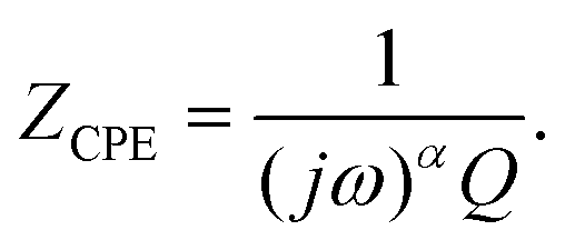 | (4) |
We used Nova 2.1 software to fit the impedance data to obtain CPE, Rf and Re. The CPE represents the capacitive nature of the electrode/electrolyte interface, also known as the double layer capacitance (Cdl), which shows frequency dispersion and cannot be modelled as a pure capacitor. Nonetheless, an effective double layer capacitance value (in Farads) is necessary to use in equivalent circuit modelling to assess the pulse response of the system. To this end, we use the CPE model developed by Brug et al.45 for a surface distribution of capacitances, potentially due to an inhomogeneous interface, to calculate an effective double layer capacitance for the blocking electrode system. Following this model, eqn (5) is used for calculating the effective capacitance.44 By replacing the CPE element in the blocking equivalent circuit with an ideal capacitor of value equal to Ceff we are able to predict how the double layer capacitance will filter a voltage-controlled pulse source or charge with a current-controlled pulse source using LTspice® software (Analog Devices, USA), a standard circuit simulator.
| Ceff = Q1/αRe(1 − α)/α. | (5) |
Reactive accelerated aging test
Reactive accelerated aging test (RAAT) was adapted from the protocol developed by Takmakov et al.33 (see the photograph of the setup in Fig. S2†). Briefly, 750 ml of 20 mM hydrogen peroxide (H2O2, Chem-Lab, Belgium) solution in phosphate saline buffer (PBS tablets, EMD Millipore, Germany) was prepared and place in a double-walled jacketed bottle (reaction chamber) (Duran®, Germany). The temperature of the reaction chamber was maintained all the time at 85 °C using a water bath with immersion thermostat heater and circulating pump (B.Braun, Frigomix, FX-U 0625). The half-life of hydrogen peroxide at 85 °C in the condition of our setup was measured as ∼96 min (see Fig. S3†); therefore, the loss of H2O2 must be compensated in order to maintain the concentration of the reaction chamber in the range of 10 to 20 mM. For that, we repetitively added concentrated hydrogen peroxide (750 mM) and removed the excess volume. We used the first-order kinetic equation to calculate the amount of the concentrated H2O2 needed to recover the concentration of the reaction chamber and maintain it during the desired time. Based on this equation we developed a calculator with MATLAB (MathWorks Inc., USA) to adjust the duty cycle of pumps and the velocity of injection and removal of the excess solution to control the setup and fine-tune the parameters (see ESI†). A peristaltic pump (Miniplus 3, Gilson) at velocity of 1.84 ml min−1 was used to deliver 9.2 ml h−1 of 750 mM H2O2 in PBS from the reservoir bottle to the reaction chamber. The duty cycle of the delivery pump was 1.25 min ON/13.75 min OFF, controlled by a timer (Talento-121, GRÄSLIN, Germany). The excess volume of 36.8 ml was removed from the reaction chamber and collected in the waste bottle every 4 hours using additional peristaltic pump (Minipump Lab S3, Shenchen, China) at the velocity of 2.45 ml min−1. The duty cycle of collection pump was set at 15 min ON/225 min OFF controlled by a timer (Heschen, CN101A). The concentration of the reaction chamber was monitored at least once a day by taking samples of 300 μl. To measure the concentration of H2O2, classical titanium oxalate assay was used. Samples were diluted 5 times in PBS and mixed with titanium(IV) oxysulfate sulfuric acid (Sigma-Aldrich) at a ratio of 1![[thin space (1/6-em)]](https://www.rsc.org/images/entities/char_2009.gif) :1 and the absorbance was measured at 410 nm using micro-plate reader (BMG LABTECH, FLUOstar OPTIMA, Germany). When the concentration of the reaction chamber is stabilized, samples were loaded to the reaction chamber using a Teflon basket and kept for 12 days and 22 hours to mimic 1-year in vivo implantation. This duration calculated using AAT calculator.46
:1 and the absorbance was measured at 410 nm using micro-plate reader (BMG LABTECH, FLUOstar OPTIMA, Germany). When the concentration of the reaction chamber is stabilized, samples were loaded to the reaction chamber using a Teflon basket and kept for 12 days and 22 hours to mimic 1-year in vivo implantation. This duration calculated using AAT calculator.46
Results and discussion
The morphology of the metallic bioelectrodes is summarized in the representative scanning electron microscopy (SEM) images in Fig. 1A. Nanostructured surfaces in the form of tilted nanocolumns (NCs) have been fabricated by GLAD-MS method.35,36 For comparative study, flat thin films (TFs) have been fabricated by standard magnetron sputtering, i.e. with the substrate being parallel to the target. The NCs were fabricated with a thickness of ∼250 nm, confirmed by cross-sectional SEM images. Considering the tilted geometry that we used for deposition, the thickness is not homogeneous along the sample axis parallel to the atoms flux. However, as in our system the distance between substrate and target was quite large (∼20 cm), the thickness variation is fairly reduced (less than 20 nm in thickness for 8 mm displacement). Therefore, the variation of the NCs thickness along the sample is less than 10%. TFs were fabricated with a thickness of ∼30 nm, confirmed with ellipsometry. The thickness of conductive films may influence the resistivity of the electrodes. It has been shown that electrical properties of Pt and Au TFs with a thickness larger than ∼15 nm are similar to those of the bulk material.47,48 Therefore, the thickness of 30 nm for control groups (TFs) is reasonable. Moreover, we compared the impedance of 30 and 100 nm thin films and obtained similar results, which supports our assumption. Interestingly, although NCs are fabricated by the same method, each metal shows a unique morphology and inclination angle β, Fig. 1A. The fabrication of nanocolumns with GLAD-MS is not straightforward, since several factors influence the deposition process (e.g., the ratio between sputtered ballistic atoms and thermalized ones, intensity of the plasma regime, the use of collimators, and the geometry of the targets).37–39 We used a weak plasma regime where the obtained inclination angle for the nanocolumns (β) mainly depends on the influence of kinetic-energy induced relaxation processes:39 the higher the influence, the more vertical the nanocolumns. Relaxation processes have maximum and minimum importance in Ti and Au respectively; thus β is 20° for Ti and 55° for Au.37,40 The obtained inclination angle for Pt is 50°, close to the value obtained for Au as expected from their proximity in the periodic table. The shape and size of NCs are distinctive for each metal. Ti NCs display a well-defined columnar structure with terraces and average diameter of 54 ± 16 nm. Conversely, Au NCs are less-distinctive, less homogeneous in size and appear in large bundles with diameter of 150 ± 44 nm. Pt NCs, although still appearing in bundles, are clearly distinctive and the narrowest (26 ± 15 nm). In spite of these specific morphological variations, we believe that the columnar structures and dimensions are similar enough to allow a fair comparative assessment.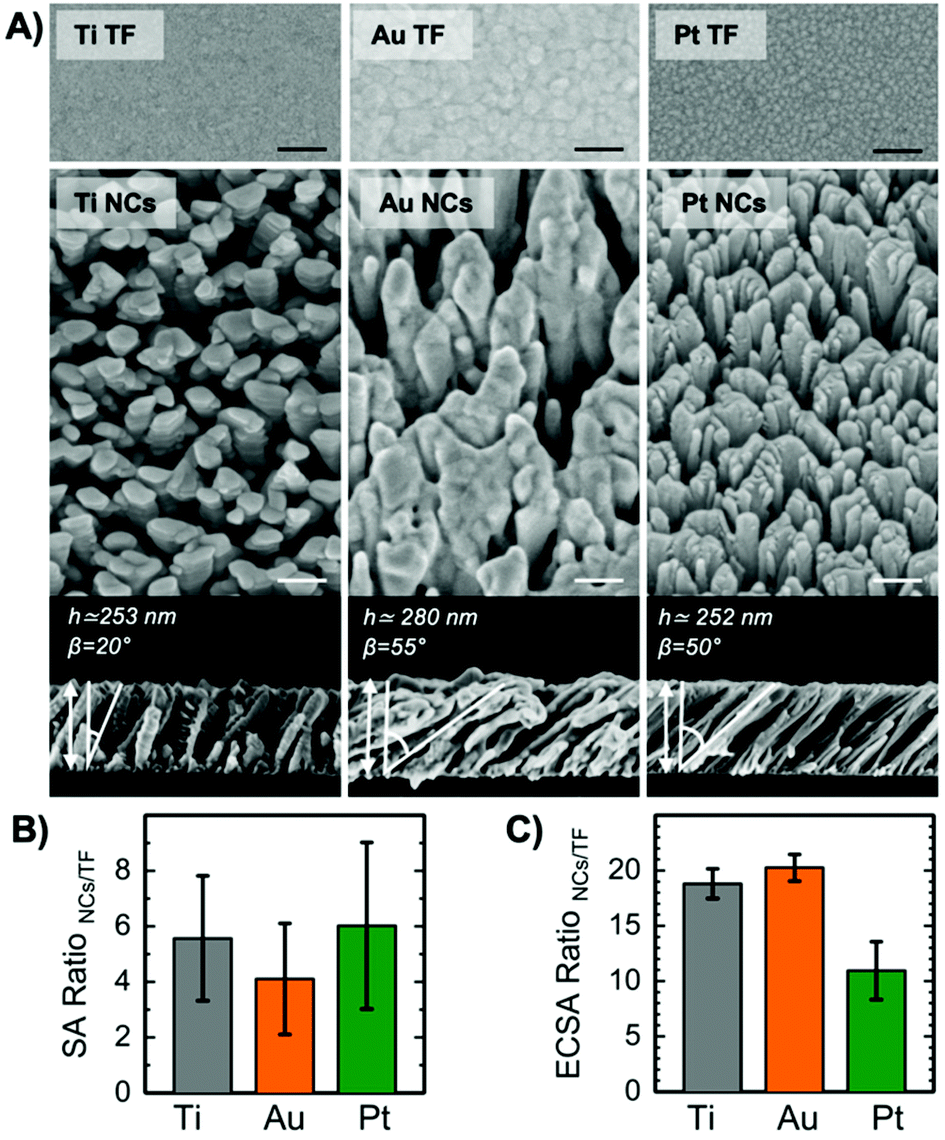 | ||
| Fig. 1 Morphological characterization of nanocolumns and thin films. (A) Scanning electron microscopy (SEM) images of nanocolumns and thin films. First and second rows are top view images of Ti, Au, and Pt thin films and nanocolumns, respectively (scale bar = 100 nm). The cross-sectional views of nanocolumns are presented in the third row. (B) Ratio between the estimated surface area of NCs and TFs (SA ratio NCs/TFs). (C) Ratio between electrochemically active surface area of NCs and TFs (ECSA Ratio NCs/TFs). | ||
Nanostructuration increases surface area. From the SEM images, we have estimated the ratio between the surface area of NCs and TFs (Fig. 1B). The results show that the amplification is at least 4 times. Nanotopographical features expose larger amount of surface area to the electrolyte at the interface, and consequently, they dramatically affect the impedance (Z). Fig. 2A and B show Bode plots (magnitude of Z vs. frequency in log scale) of all NCs and TFs. The Z of Ti, Au and Pt NCs are significantly lower than those of their corresponding thin films. It has been discussed previously that larger surface area in neural electrodes gives rise to reduced Z and increased charge injection capacity. Boehler et al. showed that the impedance of neural implants using grass-like nanostructured Pt electrodes is significantly reduced compared to thin films.49 For Ti and Pt NCs, Z at low frequencies (∼1–100 Hz) is about one order of magnitude smaller compared to Ti and Pt thin films; this value for Au NCs is about 2 times smaller compared to Au TF. The average Z calculated from several replicated experiments at frequencies of 1, 40, and 1000 Hz is shown in Fig. S5.† At higher frequencies Z converges to a value around 100 Ω for all metals and morphologies. Indeed, the shape of all Bode plots correlates with the typical electrochemical behaviour of metal electrodes in saline.
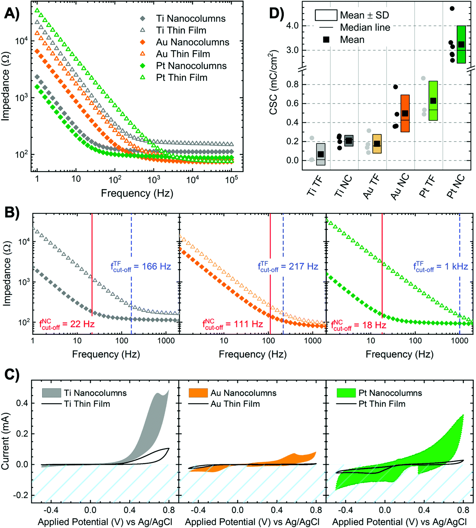 | ||
| Fig. 2 Electrochemical characterization of nanocolumns and thin films. (A and B) Representative electrical impedance Bode plots of Ti, Au, and Pt nanocolumns and thin films. (C) Representative cyclic voltammetry test results for each metallic nanocolumns and thin films. (D) Charge storage capacity for each metallic nanocolumns and thin films calculated from several measurements. | ||
At high frequencies log|Z| is mainly dominated by the resistivity of the electrolyte that is the same in all measurements (100 Ω). At intermediate frequencies, log|Z| decreases linearly, which is associated with the formation of Helmholtz double layer and capacitive charge injection. All NCs present lower values in this region compared to TFs, which indicates that the increased surface area leads to a larger capacitance of the double layer.
Fig. 1C demonstrates the ratios of electrochemically active surface area (ECSA) values between NCs and TFs for each metal. The current vs. sweep rate plots are presented in Fig. S6.† Results show that Ti, Au, and Pt nanocolumns present ∼19, 20, and 11 times more electrochemically active sites compared to their thin films, respectively. These values support the enhanced electrochemical performance of the NCs compared to the TFs. However, this result does not explain why the increase in the impedance of Au NCs compared to Au TFs is smaller than that of Pt and Ti NCs compared to their thin films. This implies that other mechanisms might be involved in the electrochemical performance of nanostructured surfaces. Moreover, ECSA ratios are larger in all cases compared to surface area ratios estimated from SEM images, Fig. 1B. In addition, ECSA and SA ratios for each metal do not follow the same trend. This can be explained through the presence of nanotopographical features on the lateral surface of the nanocolumns that are disregarded in the image analysis due to the simplicity of our estimation model.
In another attempt to quantify the nanotopography, we measured the root mean square (RMS) roughness values of NCs and TFs from Atomic Force Microscopy (AFM) images, Fig. S7 and Table S1.† However, it should be noted that the RMS roughness obtained for NCs is always underestimated since the scanning AFM tip cannot penetrate down to the substrate in every inter-columnar space due to the high aspect ratio of those features.50 RMS values summarized in Table S1† reveal that the roughness of Ti, Au, and Pt NCs are at least 42, 67 and 73 times larger than that of TFs, respectively. Once again, we found no straightforward relation between nanoroughness and impedance. Overall, although the increase in surface area (confirmed by all three techniques) improves the electrochemical performance of electrodes, dissimilar trends among the techniques implies the additional role of intrinsic properties of the material (such as electrical properties, surface chemistry and wettability).
Moreover, we observed that the cut-off frequency (fcut-off) is dramatically decreased when nanocolumns are used: fcut-off of Pt and Ti NCs are as small as ∼15 Hz. fcut-off is the frequency where the phase angle of complex Z is −45° and marks the transition from decreasing linear part to plateau in Bode plot. Above this frequency, the capacitance of the double layer does not longer dominate the impedance of the system and signals do not experience non-linear distortion. Boehler et al. already pointed out that fcut-off is an important value to be reported since it describes the competence of the system for accurate signal delivery.51 Therefore, a system with lower fcut-off values offers highly accurate signal transition for broader range of frequencies.
We performed cyclic voltammetry (CV) on each electrode, Fig. 2C, and calculated the charge storage capacity (CSC), Fig. 2D, using the integral of the cathodic current during the first CV cycle. The CSC is an indicator for the sum of the charges that can be introduced to ECF at the electrode/electrolyte interface.12 Pt in both NCs and TF configurations present the highest CSC values. CSC highly depends on the intrinsic properties of the material. Pt displays a pseudocapacitive behaviour, due to reversible faradaic reactions at the interface (e.g., Pt + H2O ⇄ PtO + 2H+ + 2e− and Pt + H2O + e− ⇄ Pt–H + OH−) that boosts safe electron injection to electrolyte.11,52 Moreover, we observed that the CSCs values are significantly improved when NCs are used: two-fold for Ti and Au and four-fold for Pt. Therefore, larger surface area significantly improves the CSC.
Reduced Z and increased CSC are favourable characteristics for stimulation systems both for in vivo implants and in vitro setups. When the impedance of a system is smaller, lower voltage is required for producing effective current. Therefore, a system with lower Z works within a smaller voltage window, which prevents harsh irreversible faradaic reactions such as the reduction (2H2O + 2e− → H2↑ + 2OH−) and the oxidation (2H2O → O2↑ + 4H+ + 4e−) of water that could considerably alter the pH of the ECF.11 Irreversible reactions for biological systems are not only limited to water electrolysis. Other molecules such as ascorbic acid, which is found in brain tissue, can be oxidized at lower potentials (E1/2 = 0.25 V vs. Ag/AgCl) than water (E1/2 = 1.03 V vs. Ag/AgCl).53 This is a critical consideration for current-controlled systems in which the applied signal can cause the resulting voltage to surpass the biologically safe potential window. Lower impedance provides the possibility to apply effective current in a smaller voltage window. In voltage-controlled systems, the applied voltage is controlled and kept in the safe potential window, however the signal can be filtered by the capacitance of the double layer.
To assess the performance of our materials as electrodes in voltage and current controlled systems, we turn to simulation. First, we fit the impedance data to a Randles circuit with a constant phase element (CPE) in parallel with a resistor (Rf) to model capacitive and faradaic charge transfer mechanisms at the electrode/electrolyte interface, Fig. 3A. Note that the charge transfer resistance was too large and thus was excluded from subsequent modelling. From the CPE, which represents the double layer effect, we calculated the effective capacitance of the double layer for each material (Ceff) following a procedure fully described in the Experimental section. The Ceff average values calculated for each material and morphology are shown in Fig. 3B. Ceff is significantly increased when NCs are used. In particular, the Ceff of Pt NCs is more than 20 times larger than that of Pt TFs. This value is ∼2 and ∼14 times larger for Au NCs and Ti NCs compared to their TFs, respectively. Ceff is normalized by the geometrical area of the samples and is used for modelling specific scenarios described next. We simulated the behaviour of both NCs and TFs in hypothetical current- and voltage-controlled systems using the equivalent circuit model of a capacitor in series with a resistor.
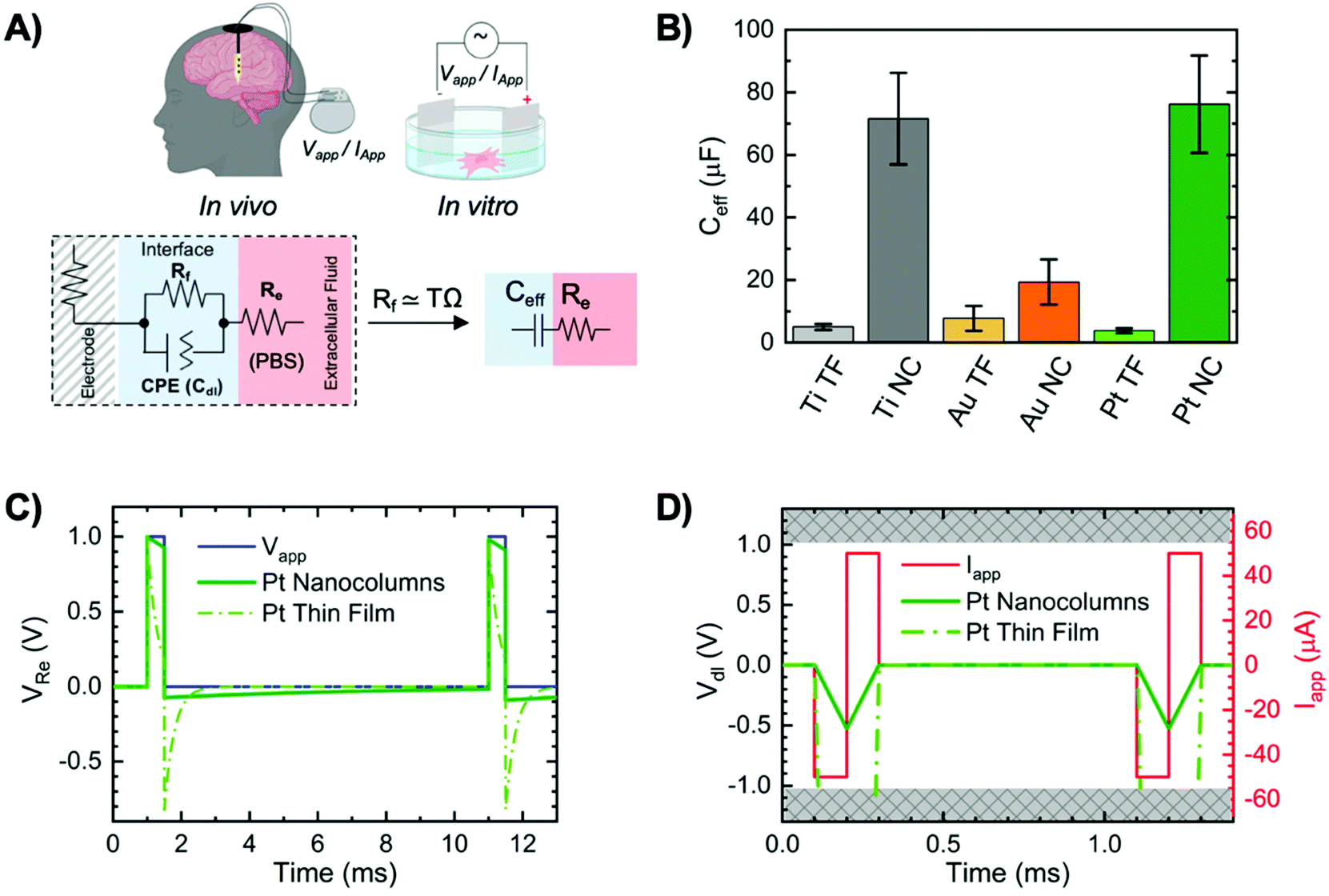 | ||
| Fig. 3 Simulation of performance of NCs and TFs in current- and voltage-controlled systems. (A) Randles circuit (left) and simplified equivalent circuit (right), for both in vivo and in vitro systems. Rf represents faradaic reactions at the interface and the constant phase element (CPE) represents the double layer. Re corresponds to the resistivity of the electrolyte. (B) Calculated effective capacitance (Ceff) for each metal. (C) Simulation of Pt NCs and TF electrode behavior in a voltage-controlled system when a pulse of 1 V is applied. Signal distortion is significantly higher for TF compared to NCs. (D) Simulation of Pt NCs and TF electrode behavior in a current-controlled system when a biphasic signal of 50 μA is applied. The voltage across the double layer exceeds −1 V (surpassing water splitting window) when TF is used. In case of NCs, a peak of voltage at −0.5 occurs that is in the biologically safe stimulation window. | ||
Voltage-controlled systems are commonly used for delivering pulsed electric fields to cells in culture (in vitro) to assess its effect on cellular processes.5,54,55 In our simulation, we chose a value for the electrolyte resistance Re to be 100 Ω, which is comparable to the conditions that occur in standard in vitro setups. We scaled Ceff to be accurate for the geometrical surface area of the commercially available Ion Optics56 electrodes. In a voltage-controlled system, a pulse voltage is applied (VApp) and we measured the voltage across the electrolyte (VRe). In Fig. 3C we demonstrate the result of such transient electrical simulation for Pt NCs compared to Pt TF electrodes (results for Au and Ti showed similar trends, Fig. S8†). We showed the signal delivered by NCs remains closer to the applied signal compared to TFs. The double layer capacitance filters the voltage across the system and causes distortion in the delivered voltage. If Ceff is a large value, the filtering effect is small because the time needed for the double layer to charge is long and the majority of the voltage drop occurs over the electrolyte during the voltage pulse.
Current-controlled systems are commonly used for in vivo neural stimulation with micro-scale implantable electrodes in the brain or nerves.14 In a current-controlled system, a biphasic current pulse is applied (IApp) to provide charge balance and the charge per phase is a critical measure for safety and biocompatibility.57,58 To visualize the electrochemical restrictions of a system that relates to charge per phase limits, we measure the voltage across the double layer capacitor (Vdl) for equivalent circuit parameters that reflect Re and Ceff for a 50 μm diameter electrode, which is a typical size for electrodes in neural implants. Using a Ceff value scaled for the geometrical area of such electrode and an Re of 50 kΩ, Fig. 3D shows the voltage across the double layer (Vdl) for a Pt NCs and TF electrodes. With the same current pulse, Vdl surpasses the water window in case of TF, and it remains in the safe potential window in case of NCs, thus showing that nanostructured electrodes offer a much greater “safe” range of operation regarding current amplitude and pulse width.
The durability and long-term performance of bioelectrodes that are implanted inside the body (in vivo) are challenged by foreign body reactions (FBR).59 FBR and inflammatory responses are triggered by several factors, mainly the implantation procedure (surgical incisions), and reactions to the material used for electrodes and packaging of the electronics (e.g., Parylene C).60 During FBR, immune cells, such as monocytes and macrophages are recruited and activated at the implantation site. Through the activation, macrophages release reactive oxygen species (ROS). This is also known as immune cells respiratory burst that leads to oxidative stress.61 ROS affects the long-term performance of neural implants both in central and peripheral nervous system by increasing corrosion and delamination in both packaging and electrode biomaterials.62 Accelerated aging tests (AATs), where high temperature is used to fasten chemical reaction kinetics, have been previously developed to predict the life time of medical devices implanted in the body or stored at room temperature.63 For instance, soaking a biomaterial in PBS at 60 °C induces an acceleration factor of 4.92 compared to the body temperature (37 °C), and a factor of 11.31 compared to storage at 25 °C.51 Recently, reactive accelerated aging test (RAAT) has been developed as an FDA approved method for testing the durability of neural implants in vivo.34 In RAAT, a 20 mM H2O2 solution in PBS is used at 80 °C to mimic several months of implantation considering FBR.33 Although RAAT is considered to be a pessimistic setup, it has been proved to be relevant in mimicking the oxidative stress caused by immune responses.33,62,64 Although studies using RAAT are generally focused on the durability of the device as a whole and corrosion of packaging biomaterials, we consider RAAT also as a useful method to study the durability of metallic electrodes. In particular, monitoring changes in electrochemical properties of electrode biomaterials after aging is a relevant factor to study. We have run a RAAT during ∼13 days on all NCs and TFs, mimicking one year of implantation in vivo. Fig. 4A shows the SEM images of the surfaces after aging. Ti NCs peeled off after RAAT probably due to the severe oxidative reaction. Ti TF, which is not as porous as Ti NCs, stayed attached to the substrate, however it was affected the most among the other samples. Several deep holes and delaminated areas are observed on abundant places at the surface. We hypothesized that accelerated formation of TiO2 during aging caused these effects. We backed up this hypothesis by performing Raman spectroscopy of Ti TFs before and after RAAT and showed the increase in presence of anatase (TiO2) in the aged samples (Fig. S9†). The fact that we have observed an increase in the amount of anatase explains a possible reason for delamination of NCs. Crystalline unit cell of TiO2 is larger than that of Ti, therefore the formation of anatase increases stress and strain of the lattice structure, which consequently gives rise to micro-crack growth, fracture, and delamination. Due to its superior surface area, higher amount of anatase forms on NCs that makes Ti nanostructured surfaces become more vulnerable compared to TFs.
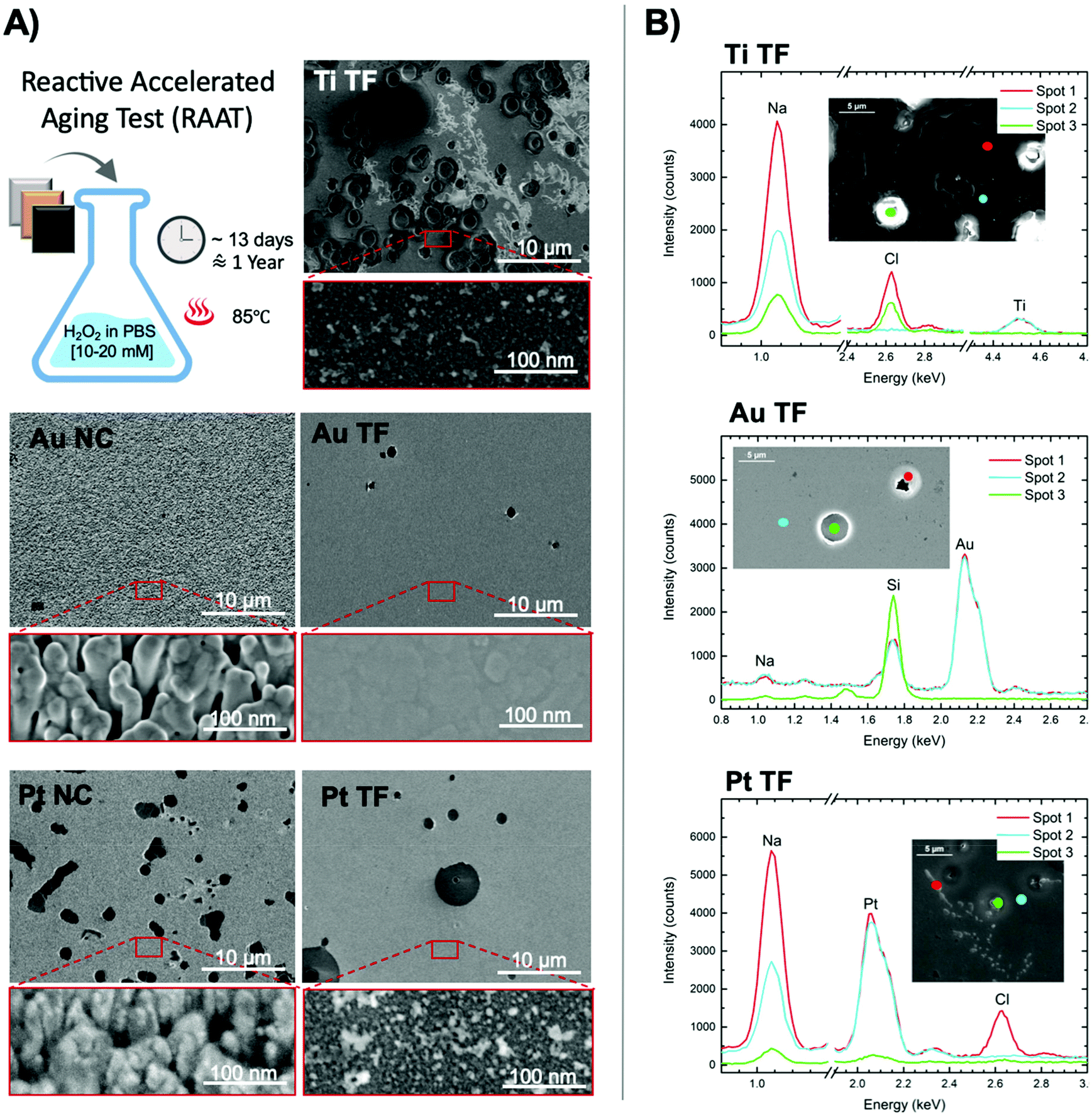 | ||
| Fig. 4 Morphological and elemental analysis of NCs and TFs after reactive accelerated aging test (RAAT). (A) SEM images of Au, Ti and Pt NCs and TFs after RAAT mimicking 1-year implantation in vivo. (B) Elemental analysis by EDX of the precipitates found on TFs. NaCl from PBS precipitates on Ti and Pt TFs but not on Au. | ||
In clear contrast, Au endured RAAT particularly well. The microstructure of Au NCs appeared fairly unchanged, which was even slightly better than the Au TFs. Although continuous heating at 85 °C caused grain size enlargement in Au TF (shown by SEM, Fig. S11†) and likely in Au NCs, there is no other obvious defect found except than tiny sporadic micro-pits. Micro-pits also appeared on Pt TFs and more on Pt NCs after aging. The full delamination of the metal within the micro-pit area is confirmed by EDX point analysis, Fig. 4B. Overall, NCs (except Ti that delaminated because of oxidation) endured the harsh condition of the RAAT better than anticipated despite their porous structure. However, there is a slight degradation of Pt NCs that is not observed in Au NCs. Also, interestingly NCs did not get contaminated by NaCl precipitates sourcing from the PBS solution. We detected NaCl precipitates on Ti TFs and Pt TFs and NCs, but not on Au TFs and NCs, Fig. 4B (for more details and details on NCs see Fig. S10, S12, S13, S14 and S15 in ESI†).
We also performed RAAT with interruptions (putting the sample in and taking it out every 3 days and 5 hours that is equivalent to 3 months in vivo), to study the evolution of the aging. We samples is generally less severe when the test is not continuous, though the results follow the same trend. Mainly, we observed less blister-like defects and pits in samples aged with interruptions compared to the continuous aging. Noticed that the effect of aging on the microstructures of all We assign this effect to the formation and burst of large gas bubbles on the surface of the samples when the system is not disturbed. The bubbles are made in result of the H2O2 fast decay at 85 °C in RAAT condition. Therefore, we also agree with Boehler et al.51 that RAAT is a pessimistic scenario for mimicking in vivo conditions because it produces some effects (such as bubble burst and micro-pit generation) that are not relevant in vivo.
We measured the Z and the CSC of the samples after aging and compared the data with fresh samples, Fig. 5. In Ti TFs we observed that the Z increased in the aged sample probably due to the precipitates on the surface. The CSC value, although still negligible, increased up to 7 folds possibly due to presence of TiO2 that is shown to have pseudocapacitive behaviour.65 For Au NCs and TFs, we obtained similar Z values before and after aging, however the equivalent circuit parameters were slightly changed (Table S2†). In the aged Au TFs, Rf reduced dramatically indicating the presence of new faradaic reactions. Before aging, Rf was extremely large (∼T Ω) that implies no faradaic charge injection. After aging, Rf is around 20 kΩ, which suggests the presence of new faradaic pathways. The CSC remained almost unchanged for Au NCs and TFs. The Z for Pt NCs remains fairly stable after RAAT, showing high reliability of Pt NCs even after exposing to the harsh conditions of RAAT. The CSC of both Pt NCs and TFs decreased possibly due to the presence of regions with delamination and pitting after aging. Overall, the outcome of exposing metallic NCs to RAAT was not predictable. Yet, in each metal the leading mechanism appears to be different. Ti NCs didn't survive RAAT because they were highly susceptible to oxidation due to their large surface area. Pt and Au NCs, being chemically inert, were not influenced by oxide/peroxide reactions; however, we assume that their surface tension properties played a role in pit formation and precipitate accumulation, which result in minor changes in electrochemical properties.
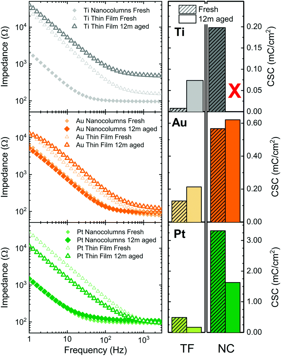 | ||
| Fig. 5 Electrochemical characterization of NCs and TFs after RAAT. (Left) Impedance Bode plots and (right) charge storage capacity of Ti, Au and Pt before and after reactive accelerated aging. | ||
Conclusions
We introduced a unique scalable fabrication method for developing nanostructured metallic surfaces with ultra-high purity that is useful for developing advanced stimulation and recording bioelectrodes for in vivo and in vitro applications. We ran a comparative study between three biocompatible metals (Ti, Au, Pt) with nanocolumnar morphology and thin films of the same metals. Overall, Pt NCs demonstrates the most improved impedance results compared to Pt thin films and other metals and morphologies. Pt NCs also revealed spectacular charge storage capacity compared to the other materials and structures that were tested in this study. Our experimental and simulation data together showed that a current-controlled system with nanocolumnar electrodes provides biologically safer (larger operation voltage and larger water window) stimulation compared to thin films. Signal delivery in a voltage-controlled system is more accurate when NCs are used. The electrical impedance and the charge storage capacity are significantly improved when nanostructures are used, because of the increase in surface area. The influence of specific nanocolumns parameters, such as length or inclination is a subject for future research. Besides, we observed that the intrinsic electrical and chemical properties of each metal play an important role. For example, Ti NCs revealed a significant improved CSC compared to Ti TFs, but this value is an order of magnitude smaller than CSC of Pt TFs.Another part of this study was dedicated to reactive accelerated aging test for estimating the stability of these metallic NCs after implantation. Interestingly, in spite of their porous structure, noble metal nanocolumns (Au and Pt) stand the harsh condition of oxidative aging fairly well and their morphological and electrochemical properties did not change significantly. Ti behaved differently and was affected by the aging test due to severe oxidation and delamination. Overall, we showed that noble metal nanostructures are durable and effective candidates for fabrication of bioelectrodes with improved electrochemical properties. These nanostructures that are produced by a scalable and economical method (GLAD-MS), can safely and advantageously replace thin films in fabrication of bioelectrodes. Although these data were obtained with electrodes in no contact with living tissues or cells, they provide a good approximation for the future application of these materials as bioelectrodes in vivo and in vitro.
Author contributions
SM, MUG, OC, EEP, JMGM contributed in conceptualization, data acquisition, methodology, validation and visualization. SM contributed in writing the original draft and funding acquisition. SM and MUG contributed in supervision and investigation. SM, JMGM and MMG contributed in funding acquisition. All authors contributed in review and editing of the original draft.Conflicts of interest
There are no conflicts to declare.Note added after first publication
This article replaces the version published on 10th February 2022 and corrects an error in Equation 5, which was previously displayed as Ceff = Q1/αRe(1 − α)/α.Acknowledgements
This work was supported by European Commission (Ref. 793102-NeuPES-H2020-MSCA-IF-2017), Comunidad de Madrid (Atracción de Talento Programme, Modalidad-1 Ref. 2019-T1/IND-1335), and CSIC (ILINK+2020 Ref. LINKA20342). The authors would also like to acknowledge the service from the MiNa Laboratory at IMN, funded from CM (project SpaceTec, S2018/NMT-4291 TEC2SPACE), MINECO (project CSIC13-4E-1794), and EU (FEDER, FSE). O. C–C and M. M-G would like to acknowledge financial support from project MAT2017-86450-c4-3-r.We specially thank Dr Aurelio Hidalgo for his support on part of the equipment used in the accelerated aging test, and Blanca Limones for her technical assistance in SEM imaging, accelerated aging test, and electrochemical characterization.
References
- B. S. Spearman, V. H. Desai, S. Mobini, M. D. McDermott, J. B. Graham, K. J. Otto, J. W. Judy and C. E. Schmidt, Adv. Funct. Mater., 2018, 28, 1701713 CrossRef.
- B. Reid and M. Zhao, Adv. Wound Care, 2014, 3, 184–201 CrossRef PubMed.
- L. Leppik, H. Zhihua, S. Mobini, V. Thottakkattumana Parameswaran, M. Eischen-Loges, A. Slavici, J. Helbing, L. Pindur, K. M. C. Oliveira, M. B. Bhavsar, L. Hudak, D. Henrich and J. H. Barker, Sci. Rep., 2018, 8, 6307 CrossRef PubMed.
- A. Mansoorifar, A. Koklu, S. Ma, G. V. Raj and A. Beskok, Anal. Chem., 2018, 90, 4320–4327 CrossRef CAS PubMed.
- S. Mobini, L. Leppik, V. T. Parameswaran and J. H. Barker, PeerJ, 2017, 5, e2821 CrossRef PubMed.
- G. Blume, W. Müller-Wichards, C. Goepfert, R. Pörtner and J. Müller, Open Biomed. Eng. J., 2013, 7, 125–132 CrossRef PubMed.
- J. Müller, M. Ballini, P. Livi, Y. Chen, M. Radivojevic, A. Shadmani, V. Viswam, I. L. Jones, M. Fiscella, R. Diggelmann, A. Stettler, U. Frey, D. J. Bakkum and A. Hierlemann, Lab Chip, 2015, 15, 2767–2780 RSC.
- L. Ni, P. KC, E. Mulvany, G. Zhang and J. Zhe, Biomed. Microdevices, 2019, 21, 20 CrossRef PubMed.
- T. Zheng, Z. Zhang, R. Zhu and D. Sun, Lab Chip, 2020, 20, 373–383 RSC.
- L. Guo, Front. Neurosci., 2016, 10, 599 Search PubMed.
- D. R. Merrill, M. Bikson and J. G. R. Jefferys, J. Neurosci. Methods, 2005, 141, 171–198 CrossRef PubMed.
- N. Chen, L. Tian, A. C. Patil, S. Peng, I. H. Yang, N. V. Thakor and S. Ramakrishna, Nano Today, 2017, 14, 59–83 CrossRef CAS.
- H. Cao, B. J. Kang, C. A. Lee, K. K. Shung and T. K. Hsiai, IEEE Trans. Biomed. Eng., 2015, 8, 114–124 Search PubMed.
- S. F. Cogan, Annu. Rev. Biomed. Eng., 2008, 10, 275–309 CrossRef CAS PubMed.
- S. Meijs, M. Fjorback, C. Jensen, S. Sørensen, K. Rechendorff and N. J. M. Rijkhoff, Front. Neurosci., 2015, 9, 268 Search PubMed.
- S. F. Cogan, J. Ehrlich, T. D. Plante, A. Smirnov, D. B. Shire, M. Gingerich and J. F. Rizzo, Conf. Proc. IEEE Eng. Med. Biol. Soc., 2004, 6, 4153–4156 Search PubMed.
- A. A. Schendel, K. W. Eliceiri and J. C. Williams, Curr. Opin. Solid State Mater. Sci., 2014, 18, 301–307 CrossRef CAS PubMed.
- N. Tandon, C. Cannizzaro, P.-H. G. Chao, R. Maidhof, A. Marsano, H. T. H. Au, M. Radisic and G. Vunjak-Novakovic, Nat. Protoc., 2009, 4, 155–173 CrossRef CAS PubMed.
- G. M. Xiong, A. T. Do, J. K. Wang, C. L. Yeoh, K. S. Yeo and C. Choong, J. Biol. Eng., 2015, 9, 14 CrossRef PubMed.
- R. A. Gittens, R. Olivares-Navarrete, R. Rettew, R. J. Butera, F. M. Alamgir, B. D. Boyan and Z. Schwartz, Bioelectromagnetics, 2013, 34, 599–612 CrossRef CAS PubMed.
- F. Buch, T. Albrektsson and E. Herbst, Biomaterials, 1984, 5, 341–346 CrossRef CAS PubMed.
- L. M. Bins-Ely, E. B. Cordero, J. C. M. Souza, W. Teughels, C. A. M. Benfatti and R. S. Magini, J. Periodontal Res., 2017, 52, 479–484 CrossRef CAS PubMed.
- S. Arcot Desai, J. D. Rolston, L. Guo and S. M. Potter, Front. Neuroeng., 2010, 3, 5 Search PubMed.
- Y. H. Kim, G. H. Kim, A. Y. Kim, Y. H. Han, M.-A. Chung and S.-D. Jung, J. Neural Eng., 2015, 12, 066029 CrossRef PubMed.
- C. A. Marrese, Anal. Chem., 1987, 59, 217–218 CrossRef CAS.
- C. A. R. Chapman, H. Chen, M. Stamou, J. Biener, M. M. Biener, P. J. Lein and E. Seker, ACS Appl. Mater. Interfaces, 2015, 7, 7093–7100 CrossRef CAS PubMed.
- A. Panepinto and R. Snyders, Nanomaterials, 2020, 10, 2039 CrossRef CAS PubMed.
- R. Alvarez, S. Muñoz-Piña, M. U. González, I. Izquierdo-Barba, I. Fernández-Martínez, V. Rico, D. Arcos, A. García-Valenzuela, A. Palmero, M. Vallet-Regi, A. R. González-Elipe and J. M. García-Martín, Nanomaterials, 2019, 9, 1217 CrossRef CAS PubMed.
- I. Izquierdo-Barba, J. M. García-Martín, R. Álvarez, A. Palmero, J. Esteban, C. Pérez-Jorge, D. Arcos and M. Vallet-Regí, Acta Biomater., 2015, 15, 20–28 CrossRef CAS PubMed.
- M. Martín, P. Salazar, R. Álvarez, A. Palmero, C. López-Santos, J. L. González-Mora and A. R. González-Elipe, Sens. Actuators, B, 2017, 240, 37–45 CrossRef.
- Z. Hu, J. M. García-Martín, Y. Li, L. Billot, B. Sun, F. Fresno, A. García-Martín, M. U. González, L. Aigouy and Z. Chen, ACS Appl. Mater. Interfaces, 2020, 12, 5979–5989 CrossRef CAS PubMed.
- Y. Yang, A. V. Bazhin, J. Werner and S. Karakhanova, Int. Rev. Immunol., 2013, 32, 249–270 CrossRef CAS PubMed.
- P. Takmakov, K. Ruda, K. Scott Phillips, I. S. Isayeva, V. Krauthamer and C. G. Welle, J. Neural Eng., 2015, 12, 026003 CrossRef PubMed.
- FDA's Center for Devices and Radiological Health, ‘Catalog of Regulatory Science Tools to Help Assess New Medical Devices’, https://www.fda.gov/medical-devices/science-and-research-medical-devices/catalog-regulatory-science-tools-help-assess-new-medical-devices, (accessed April 12, 2021).
- J. C. Sit, D. Vick, K. Robbie and M. J. Brett, J. Mater. Res., 1999, 14, 11 CrossRef.
- J. M. García-Martín, R. Alvarez, P. Romero-Gómez, A. Cebollada and A. Palmero, Appl. Phys. Lett., 2010, 97, 173103 CrossRef.
- R. Alvarez, J. M. García-Martín, M. Macías-Montero, L. Gonzalez-Garcia, J. C. González, V. Rico, J. Perlich, J. Cotrino, A. R. González-Elipe and A. Palmero, Nanotechnology, 2013, 24, 045604 CrossRef CAS PubMed.
- R. Alvarez, J. M. Garcia-Martin, M. C. Lopez-Santos, V. Rico, F. J. Ferrer, J. Cotrino, A. R. Gonzalez-Elipe and A. Palmero, Plasma Processes Polym., 2014, 11, 571–576 CrossRef CAS.
- R. Alvarez, A. Garcia-Valenzuela, V. Rico, J. M. Garcia-Martin, J. Cotrino, A. R. Gonzalez-Elipe and A. Palmero, Nanotechnology, 2019, 30, 475603 CrossRef CAS PubMed.
- R. Alvarez, J. M. Garcia-Martin, A. Garcia-Valenzuela, M. Macias-Montero, F. J. Ferrer, J. Santiso, V. Rico, J. Cotrino, A. R. Gonzalez-Elipe and A. Palmero, J. Phys. D: Appl. Phys., 2016, 49, 045303 CrossRef.
- Z. Hu, P. R. Troyk and S. F. Cogan, in 2005 IEEE Engineering in Medicine and Biology 27th Annual Conference, IEEE, Shanghai, China, 2005, pp. 5246–5249.
- S. Watzele, P. Hauenstein, Y. Liang, S. Xue, J. Fichtner, B. Garlyyev, D. Scieszka, F. Claudel, F. Maillard and A. S. Bandarenka, ACS Catal., 2019, 9, 9222–9230 CrossRef CAS.
- P. Connor, J. Schuch, B. Kaiser and W. Jaegermann, Z. Phys. Chem., 2020, 234, 979–994 CrossRef CAS.
- M. E. Orazem and B. Tribollet, Electrochemical Impedance Spectroscopy, John Wiley & Sons, Ltd, 1st edn, 2008 Search PubMed.
- G. J. Brug, A. L. G. van den Eeden, M. Sluyters-Rehbach and J. H. Sluyters, J. Electroanal. Chem., 1984, 176, 275–295 CrossRef CAS.
- Accelerated Aging Time Calculator Westpak, https://www.westpak.com/resources/calculator/accelerated-aging-time-calculator/, (accessed July 5, 2021).
- J. S. Agustsson, U. B. Arnalds, A. S. Ingason, K. B. Gylfason, K. Johnsen, S. Olafsson and J. T. Gudmundsson, J. Phys.: Conf. Ser., 2008, 100, 082006 CrossRef.
- A. I. Oliva, F. López-Garduza and V. Sosa, Ingeniería, 2006, 10, 57–65 Search PubMed.
- C. Boehler, T. Stieglitz and M. Asplund, Biomaterials, 2015, 67, 346–353 CrossRef CAS PubMed.
- F. Gołek, P. Mazur, Z. Ryszka and S. Zuber, Appl. Surf. Sci., 2014, 304, 11–19 CrossRef.
- C. Boehler, S. Carli, L. Fadiga, T. Stieglitz and M. Asplund, Nat. Protoc., 2020, 15, 3557–3578 CrossRef CAS PubMed.
- E. M. Hudak, J. T. Mortimer and H. B. Martin, J. Neural Eng., 2010, 7, 026005 CrossRef CAS PubMed.
- K. P. Olczak and K. J. Otto, J. Electrochem. Soc., 2021, 168, 085501 CrossRef CAS.
- K. Srirussamee, S. Mobini, N. J. Cassidy and S. H. Cartmell, Biotechnol. Bioeng., 2019, 116, 3421–3432 CrossRef CAS PubMed.
- K. Srirussamee, R. Xue, S. Mobini, N. J. Cassidy and S. H. Cartmell, J. Tissue Eng., 2021, 12, 1–17 CAS.
- C-dish device, Ion Optics, https://www.ionoptix.com/products/components/stimulators/c-dish/, (accessed July 5, 2021).
- R. V. Shannon, IEEE Trans. Biomed. Eng., 1992, 39, 424–426 CrossRef CAS PubMed.
- D. B. McCreery, W. F. Agnew, T. G. H. Yuen and L. Bullara, IEEE Trans. Biomed. Eng., 1990, 37, 996–1001 CrossRef CAS PubMed.
- F. Lotti, F. Ranieri, G. Vadalà, L. Zollo and G. Di Pino, Front. Neurosci., 2017, 11, 497 CrossRef PubMed.
- N. de la Oliva, M. Mueller, T. Stieglitz, X. Navarro and J. del Valle, Sci. Rep., 2018, 8, 5965 CrossRef PubMed.
- J. Gaire, H. C. Lee, N. Hilborn, R. Ward, M. Regan and K. J. Otto, J. Neural Eng., 2018, 15, 066027 CrossRef PubMed.
- R. Caldwell, M. G. Street, R. Sharma, P. Takmakov, B. Baker and L. Rieth, Biomaterials, 2020, 232, 119731 CrossRef CAS PubMed.
- ASTM International, Subcommittee F02.50 on Package Design and Development, ‘ASTM F1980-16 Standard Guide for Accelerated Aging of Sterile Barrier Systems for Medical Devices’, https://www.astm.org/Standards/F1980.htm, (accessed August 30, 2021).
- M. G. Street, C. G. Welle and P. A. Takmakov, Rev. Sci. Instrum., 2018, 89, 094301 CrossRef PubMed.
- J. Wang, J. Polleux, T. Brezesinski, S. Tolbert and B. Dunn, ECS Trans., 2008, 11, 101 CrossRef CAS.
Footnotes |
| † Electronic supplementary information (ESI) available: Schematics of experimental setups; H2O2 decay plot; impedance statistics; current vs. sweep rate plots; AFM images and RMS data; transient electrical simulation for Ti and Au; Raman spectra for Ti TFs; EDX characterizations after aging; equivalent circuits for Au NCs and TFs. See DOI: 10.1039/d1nr06280h |
| ‡ These authors contributed equally to this work. |
| This journal is © The Royal Society of Chemistry 2022 |