
Carrier dynamics at trench defects in InGaN/GaN quantum wells revealed by time-resolved cathodoluminescence†
Gunnar
Kusch
 a,
Ella J.
Comish
a,
Kagiso
Loeto
a,
Simon
Hammersley
bc,
Menno J.
Kappers
a,
Phil
Dawson‡
a,
Rachel A.
Oliver
a and
Fabien C.-P.
Massabuau
*ad
a,
Ella J.
Comish
a,
Kagiso
Loeto
a,
Simon
Hammersley
bc,
Menno J.
Kappers
a,
Phil
Dawson‡
a,
Rachel A.
Oliver
a and
Fabien C.-P.
Massabuau
*ad
aDepartment of Materials Science and Metallurgy, University of Cambridge, Cambridge CB3 0FS, UK. E-mail: f.massabuau@strath.ac.uk
bPhoton Science Institute, Department of Electrical and Electronic Engineering, School of Engineering, The University of Manchester, Manchester, M13 9PL, UK
cPoro Technologies Ltd, Sawston, CB22 3JH, UK
dDepartment of Physics, SUPA, University of Strathclyde, Glasgow G4 0NG, UK
First published on 14th December 2021
Abstract
Time-resolved cathodoluminescence offers new possibilities for the study of semiconductor nanostructures – including defects. The versatile combination of time, spatial, and spectral resolution of the technique can provide new insights into the physics of carrier recombination at the nanoscale. Here, we used power-dependent cathodoluminescence and temperature-dependent time-resolved cathodoluminescence to study the carrier dynamics at trench defects in InGaN quantum wells – a defect commonly found in III-nitride structures. The measurements show that the emission properties of trench defects closely relate to the depth of the related basal plane stacking fault within the quantum well stack. The study of the variation of carrier decay time with detection energy across the emission spectrum provides strong evidence supporting the hypothesis that strain relaxation of the quantum wells enclosed within the trench promotes efficient radiative recombination even in the presence of an increased indium content. This result shines light on previously reported peculiar emission properties of the defect, and illustrates the use of cathodoluminescence as a powerful adaptable tool for the study of defects in semiconductors.
 Fabien C.-P. Massabuau | Fabien Massabuau is currently a Chancellor's Fellow (Lecturer) at the University of Strathclyde, where his group investigates the fabrication and characterisation of emerging wide-bandgap semiconductors for applications such as solar-blind photodetectors. Fabien received his Engineering Diploma from Ecole Centrale de Lyon (2011), MRes in Materials Science from Claude Bernard University Lyon 1 (2011), and PhD from the University of Cambridge (2015) on the nanostructure of InGaN/GaN quantum wells and their impact on light emitting diode performances. From 2015 to 2019, Fabien was a post-doctoral researcher at the University of Cambridge developing a multi-microscopy methodology to study defects in III-nitride semiconductors. |
Introduction
III-Nitrides are important materials for applications in optoelectronics1 and power electronics.2 This material system is however plagued by a high density of defects (point defects, dislocations, trench defects) which can potentially affect the device properties and reliability. In particular, one significant III-nitrides material challenge is the drop in light emitting diodes’ efficiency with increasing emission wavelength, often termed the “green gap”,3,4 and for which these defects have been blamed.5–7Trench defects are commonly found in a wide variety of III-nitride structures, including InGaN/GaN quantum wells (QWs),5,8–23 but also AlInGaN QWs,24 or InGaN epilayers,25–28 and have been specifically implicated as a potential cause of the “green gap”.5 These defects have been shown to consist of an I1-type basal plane stacking fault (BSF) located in the active region of the device which is bounded by a vertical stacking mismatch boundary (SMB) that propagates towards the surface and opens as a series of coalescing pits.8,14,25 The region of material enclosed by the trench arising from the coalescing pits has been reported to have different and diverse emission properties compared to the material surrounding it8–13 – within a single sample the emission of the enclosed region can be redshifted by varying degrees or even occasionally blueshifted. Also, the emission from some defects can be more intense than that from the surrounding material whilst others can be dimmer. The diversity of emission properties has been found to correlate with the position of the BSF in the QW stack and it was suggested that the emission properties could be due to the trench altering the local group-III species’ incorporation rates via a process similar to selected area epitaxy (SAE).9 To date, the carrier dynamics leading to the peculiar emission properties of the defects have not been investigated in detail.
Cathodoluminescence (CL) is a common technique for the study of the optical and microstructural properties of semiconductors and has been successfully used in the past on trench defects.8–13 In recent years, time-resolved CL has emerged as a powerful tool to extract information about carrier recombination with a high spatial resolution, making it an ideal technique for investigating extended defects.29,30 In this paper we employ time-resolved CL to study the properties of trench defects in InGaN/GaN QW structures. The combination of spatial, spectral and time-resolved dataset provides new insights into the impact of this defect on the physics of recombination.
Methods
The sample investigated here consists of a ten-period InGaN/GaN QW sample grown by metal organic vapor phase epitaxy (MOVPE) in a Thomas Swan 6 × 2-inch showerhead reactor. Trimethylgallium (TMG), trimethylindium (TMI) and ammonia (NH3) were used as precursors with H2 as the carrier gas for GaN growth and with N2 as the carrier gas for InGaN growth. GaN pseudo-substrates, consisting of ca. 5 μm of GaN grown on c-plane sapphire at 1020 °C following deposition of a 30 nm thick GaN nucleation layer at 540 °C, were employed. The InGaN QWs were grown at 747 °C using a TMG flow of 1.5 sccm and a TMI flow of 300 sccm to intentionally promote the formation of trench defects21 – resulting in a trench defect density of (2.6 ± 0.5) × 108 cm−2. The thickness and indium composition of the InGaN QWs were (2.4 ± 0.1) nm and (15.5 ± 0.5) % respectively, as determined by X-ray diffraction.31 Following the growth of the InGaN QW layer, a 1 nm GaN capping layer was deposited for 100 s at the same temperature and TMG flow rate as for the QW. The growth of GaN continued at the same flow rate while the temperature was ramped to 860 °C over 90 s. At 860 °C the TMG flow was increased to 20 sccm for 36 s resulting in an overall barrier thickness of (7.3 ± 0.1) nm as determined by X-ray diffraction.We conducted a multi-microscopy analysis similar to the one presented in ref. 9, whereby the same set of trench defects is analysed by atomic force microscopy (AFM) and CL. This approach allows us to directly correlate the morphological and optical properties of the same set of defects. AFM was conducted in tapping mode in a Bruker Dimension Icon microscope, and was used to determine the prominence and area of the enclosed region as well as the thickness of the trench (we refer the reader to ref. 9 for definitions of these metrics). CL hyperspectral mapping was performed in an Attolight Allalin 4027 Chronos dedicated CL scanning electron microscope. CL hyperspectral maps were recorded with an iHR320 spectrometer with a focal length of 320 mm, a 150 lines per mm grating blazed at 500 nm, a 7 mm entrance slit and an Andor 1024 px charged coupled device. Time-resolved CL measurements were performed by triggering the electron gun with the third harmonic of a Nd:YAG laser (355 nm) with a frequency of 40.3 MHz and a pulse width of 7 ps. All the CL time decay curves were recorded with a time-correlated single photon counting (TCSPC) setup resulting in a time resolution of ca. 100 ps (Fig. 1). CL decay times quoted in this study are given as the 1/e time, i.e. the time taken for the CL intensity to decay to 1/e of its maximum value. Fig. 1 provides a schematic of the time-resolved CL setup. To study the power dependence of the light emission, the probe current was adjusted from ca. 25 pA to 60 nA. In continuous wave mode, the gun lens was adjusted to tune the probe current from 0.6 nA to 60 nA approximately, and an additional probe current of ca. 25 pA was obtained using the electron gun in pulsed mode (note that this is the current averaged over a pulse period). The electron gun voltage was kept at 6 kV throughout the experiment to maintain an interaction volume of ca. 200 nm, according to Monte Carlo simulations.32 The properties of about 50 trench defects were studied using the approach described above.
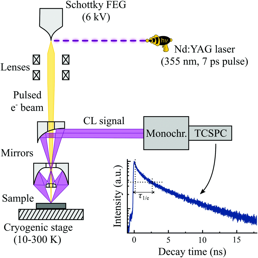 | ||
| Fig. 1 Schematic of the time-resolved CL setup. | ||
Results and discussion
Power-dependent CL
AFM and 300 K CL were carried out on the same region of the sample with the CL excitation conditions adjusted from ca. 25 pA to 60 nA, as illustrated in Fig. 2. Fig. 2(b–f) clearly shows that the integrated CL intensity of the enclosed region of the trench defects (in comparison to the surrounding material) varies with probe current: the trench defects generally become darker than the surrounding material as the probe current increases. Previous room temperature CL studies have reported that the enclosed region of trench defects could be either brighter, darker, or at the same intensity as the surrounding material.8,10,12,13,16 These studies employed low excitation conditions – for example Bruckbauer et al. used a probe current of ca. 100 pA.10,11 Our CL maps taken at low probe currents (Fig. 2(b and c)) are in agreement with these reports.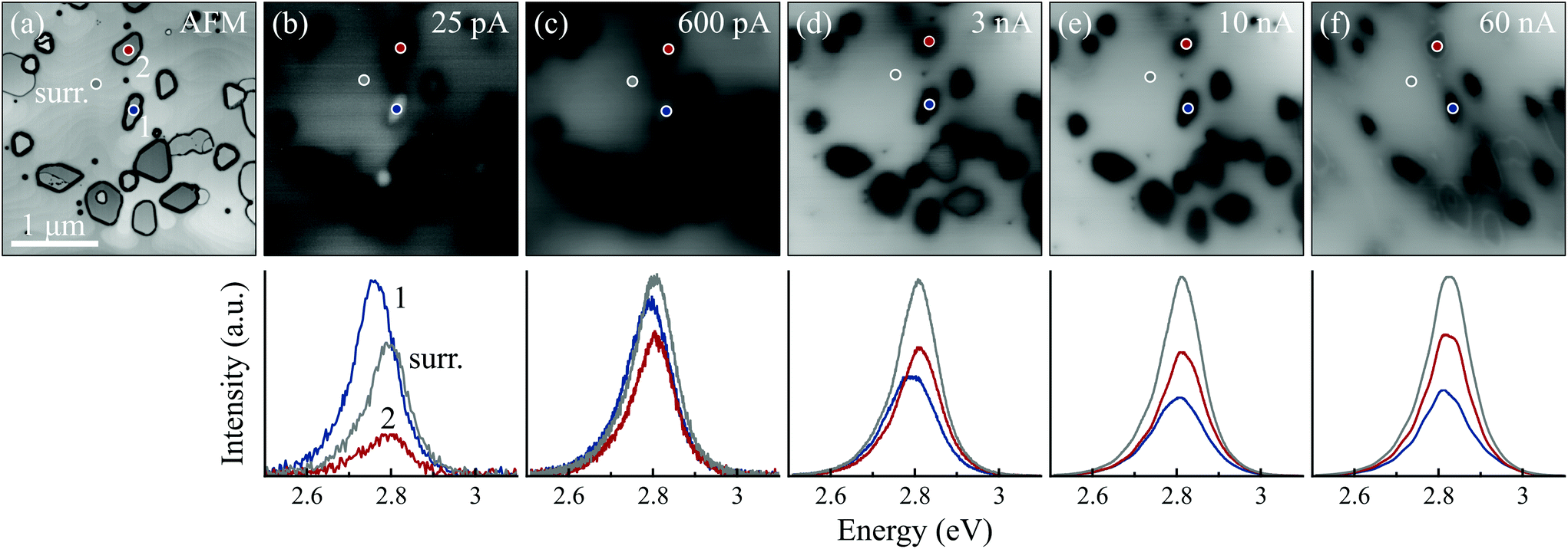 | ||
| Fig. 2 The same region of the sample observed by (a) AFM and (b–f) 300 K panchromatic CL with probe currents ranging from ca. 25 pA to 60 nA. The lower panel below each CL image shows selected spectra of trench defect 1 (blue), trench defect 2 (red) and the surrounding material (grey) which are identified in the maps in (a–f). | ||
Upon further scrutiny, these CL maps highlight two separate trends. On the one hand, one class of trench defects (e.g. defect “1” in Fig. 2) is brighter than the surrounding material under low excitation conditions and becomes relatively darker as the probe current increases – this is verified with the CL spectra in the lower panel of Fig. 2(b–f). On the other hand, a second class of trench defects (e.g. defect “2” in Fig. 2) remains relatively darker than the surrounding material irrespective of the excitation conditions. The CL spectra in the lower panels of Fig. 2 also reveal the power dependence of the spectral shift, with trench defects probed under low currents exhibiting a redshift compared to the surrounding material (in line with previous studies8,10,12), while the spectra of the emission from trench defects analysed under high currents have the same peak energies as the emission from the surrounding material. The multi-microscopy approach shows that the separate behaviours of the two categories of trench defects relate to the thickness of the trench (ESI Fig. S1†) – trench defect 1 is representative of a defect with a wide trench, and trench defect 2 is representative of a defect with a narrow trench (using the definition of the trench thickness from ref. 9, trench defects 1 and 2 have a thickness of 52 nm and 32 nm respectively, while the median thickness over the studied population is 36 nm). Correlation between the trench thickness and CL emission has been identified previously9,11 for low excitation conditions. The present study shows that a correlation between these metrics also exists at high excitation currents, although the nature of the correlation inverts with excitation conditions: with low excitation, defects with wide trenches exhibit the most intense and most redshifted emission (in line with ref. 9 and 11), whilst at high excitations, they exhibit weak emission intensity and zero redshift. We found no correlation with other morphological metrics (i.e. prominence or area of the enclosed region). Since the width of the trench is the only morphological feature linked to the optical properties (as per the present work and ref. 9 and 11), we expect that the results presented in this manuscript for trench defect 1 and 2 would still hold for other trench defects with wide and narrow trenches respectively.
Structure of trench defects
Before we go on to address the CL spectroscopy data in more detail, we need to discuss the precise nature of the CL excitation conditions and the relevant details of the QW structures alongside schematic descriptions of trench defects 1 and 2. Fig. 3 shows schematic diagrams (derived from ref. 33 and 34) of the structure of trench defects with a wide and narrow trench, as trench defects 1 and 2 respectively, along with simulations of the excitation volume of the incident CL beam.32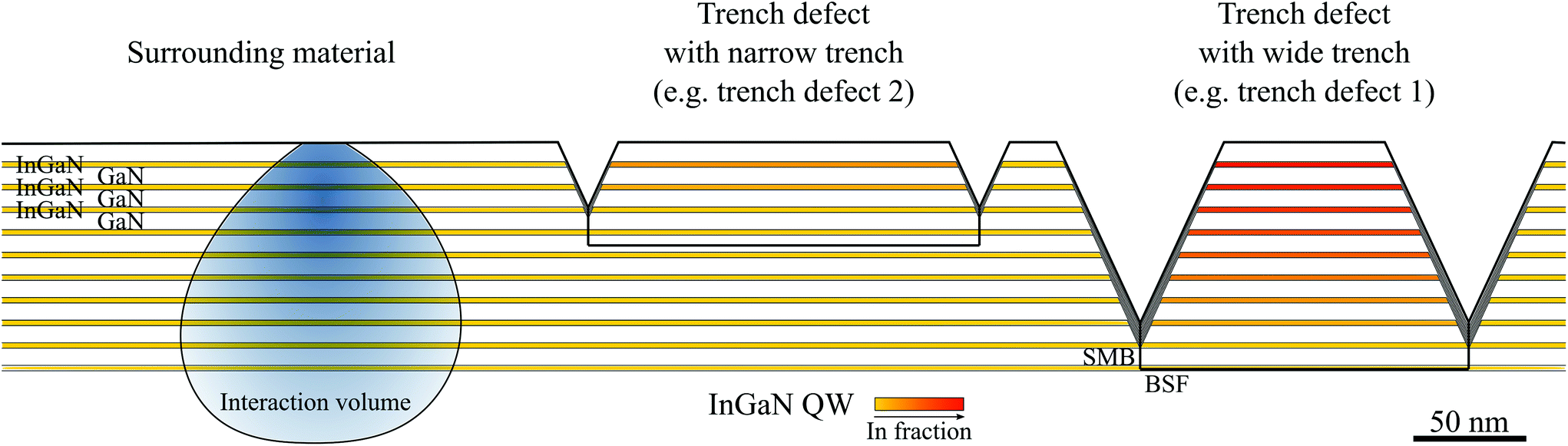 | ||
| Fig. 3 Schematic of the structural and compositional properties of the trench defects with narrow and wide trenches. The scales, although illustrative, were designed to provide an accurate representation of the system. An interaction volume was simulated32 and overlaid on the image to indicate the experimental conditions used here. A colour gradient is used to schematise the gradual increase in QW composition in the enclosed region. | ||
We will first briefly review the conclusions drawn from previous investigations as to the nature of trench defects. Our previous data suggests that all trench defects originate from an I1-type BSF located in the QW stack (which can be located either in the InGaN QWs8 or GaN barriers14). At the boundary of the BSF is a SMB, that is, a boundary between the ABABAB stacking sequence of the surrounding material and the BCBCBC stacking sequence of the enclosed material grown on top of the BSF. Northrup et al. performed first principle calculations of SMB in GaN and predicted a high domain wall energy of 105 meV Å−1.35 It is therefore expected that the SMB would not extend over long distances through the QW stack and would instead open as pits as a means of reducing its energy (a similar argument was used to explain the termination of dislocations by V-pits36). Hence, trench defects with a narrow trench (e.g. trench defect 2) stem from a BSF located near the top of the QW stack, while trench defects with a wide trench (e.g. trench defect 1) relate to a BSF located near the bottom of the QW stack – this interpretation is supported by recent transmission electron microscopy observations.33 The SMB contains threefold coordinated atoms leading to electronic states within the bandgap.35 The non-radiative nature of the recombination at the SMB was also demonstrated experimentally.9
The opening of the SMB into a trench formed from coalescing pits defines the onset of SAE effects on the growth of the enclosed material, where the trench acts as a “negative mask” for SAE growth.9 As the growth proceeds, the SAE mask (i.e. the trench) becomes gradually wider, thus leading to QWs gradually enriched in indium.37 This increase in the indium fraction of the QWs enclosed by the defect was studied by O'Hanlon et al. who used transmission electron microscopy to observe the structure of wide and narrow trench defects.33 In this work energy dispersive X-ray spectroscopy was used to show that the indium fraction of the QWs enclosed within a wide trench would gradually increase by up to ca. 4% (as an absolute change) compared to the surrounding QWs. This gradual increase in composition is represented by the colour scale in Fig. 3. That study also revealed the presence of thin sidewall QWs on the inclined facets of the trench (schematically represented in Fig. 3) and a reduction in well-width fluctuations in the enclosed QWs in comparison to the surrounding QWs (not represented in Fig. 3). The opening of the SMB as pits also allows for strain relaxation of the enclosed material.9 Strain relaxation was indeed linked to trench defect density in ref. 5.
In a trench defect with a narrow trench (e.g. trench defect 2), the BSF is located near the top of the QW stack (as illustrated in Fig. 3). Thus, a significant part of the QW stack beneath this type of trench is essentially the same as the QWs in the surrounding material. Also, we can see that the material enclosed by the defect is a small part of the probed material when we excite this type of defect (see the size of the excitation volume). In contrast, when a trench defect with a wide trench is excited (e.g. trench defect 1), we will expect a greater contribution from the QWs enclosed by the trench, where the indium fraction is larger than that of the QWs in the surrounding material.
Temperature-dependent time-resolved CL
To shed light on the carrier recombination processes at play in trench defects, we conducted temperature-dependent and time-resolved CL measurements on the enclosed region of trench defects 1 and 2 (identified in Fig. 2) which we treat as being representative of defects with a wide and narrow trench, respectively. For comparison, the same type of measurement was also taken on the surrounding material. Time decay curves were recorded at temperatures from 10 K to 300 K and probe current of ca. 25 pA.Fig. 4 presents the CL spectra and 1/e decay time across the lineshape taken at 10 K in each of the three regions of the sample. Fig. 4(a) shows the 10 K CL spectrum taken on the surrounding material as well as the 1/e decay time versus emission energy. The emission spectrum is very similar to that reported by many groups who have studied the recombination from as-grown polar InGaN/GaN QWs. The spectrum has a main peak with an emission energy of 2.83 eV along with longitudinal-optical (LO) phonon replicas at 2.74 eV and 2.66 eV. The mechanism responsible for the observed spectral features is zero phonon and phonon-accompanied recombination of localised electrons and holes.38 Using an atomistic tight binding modelling, Schulz et al. predicted that electrons and holes are independently localised in polar InGaN/GaN QWs, where the holes are localised at random alloy fluctuations, and electrons are localised near the QW top interface at well-width fluctuation sites,39 leading to the characteristic non-exponential decay shape.40 The variation of the decay time with emission energy across the zero phonon peak is also typical of that obtained on polar InGaN/GaN QWs, where the increase in lifetime with decreasing detection energy relates to compositional fluctuations and subsequently built-in electric field fluctuations in the QWs,38,41 and the reduction in the measured CL lifetime on the low energy side of the emission caused by the increasing contribution to the emission of the LO phonon replica. The lifetime of the LO phonon accompanied emission at a given photon energy has the same decay lifetime as the emission from the zero phonon line one LO phonon energy above. When the replica and the zero phonon emissions overlap as in the low energy side of the emission this results in a reduction in the measured decay time, however the lifetime of the zero phonon emission continues to increase in line with the dependence observed on the high energy side of the peak.
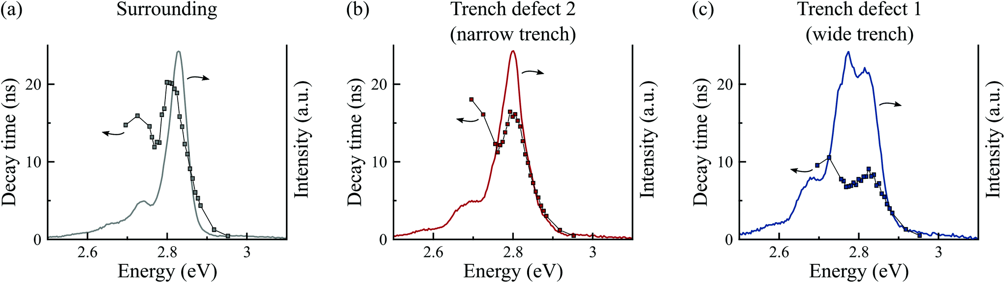 | ||
| Fig. 4 10 K 1/e decay time versus emission energy and CL spectra recorded on (a) the surrounding material, (b) trench defect 2 (narrow trench), and (c) trench defect 1 (wide trench). | ||
The data for trench defect 2 (Fig. 4(b)) are very similar to those obtained from the surrounding material (Fig. 4(a)). This is in line with the picture of trench defects with a narrow trench whereby the majority of the material probed comes from QWs located below the BSF, and therefore similar to the surrounding QWs. We note however, in comparison to the surrounding QWs, that the zero phonon peak is broader with a shallower slope on the low energy side. The decay time is also observed to be faster on the low energy side of the peak compared to that of the surrounding material. We attribute this broadening and associated faster decay to an increasing contribution towards lower energies from the QWs enclosed within the trench. As discussed earlier, these QWs are expected to have a higher indium fraction and to undergo some strain relaxation, which explains the shorter lifetime at a lower energy in comparison to that of the QWs located below the BSF.
Turning now our attention to trench defect 1 (Fig. 4(c)). We observe that the 10 K CL spectrum is different from the spectrum for the QWs in the surrounding material (Fig. 4(a)). No longer is there only one set of zero phonon and phonon-accompanied recombination channels but rather the spectrum is very broad with several distinct features. The schematic of trench defect 1 drawn in Fig. 3 suggests that there should be a greater contribution to the emission spectrum from the QWs enclosed by the trench defect where, based on the work by O'Hanlon et al., the indium fraction increases.33 On this basis we assign the peak at 2.82 eV as due to zero phonon recombination from largely unperturbed QWs below and directly above the BSF. The peak at 2.77 eV is then assigned to the QWs enclosed by the trench where the indium fraction is greater. We also identify the feature at 2.75 eV as a LO phonon replica of the peak emission at 2.82 eV and the peak at 2.68 eV as a phonon replica of the emission at 2.77 eV. To give some idea of the variation in the emission energy produced by the proposed change in indium fraction we used the results of calculations for the lowest energy transition for ideal strained QWs with thickness of 2.4 nm produced by Nextnano.42 We found that a variation of indium fraction from 15.5% to 16.5% would result in a shift in emission energy of ∼56 meV which is compatible with the difference in energy between the two zero phonon emission peak energies. We note that this variation of composition of 1% is smaller than the variation of 4% measured by O'Hanlon et al., but this could be linked to the simplicity of our simulation (including the fact that we simulated strained rather than partially relaxed QWs), the accuracy of energy dispersive X-ray spectroscopy for composition quantification, and the fact we are not analysing the same trench defect or sample as O'Hanlon et al.; this is nevertheless a very reasonable match.
The decay time is interesting in this defect; firstly we note the transient is much faster than that of the QWs in the surrounding material or trench defect 2. Moreover, the decay differs from those analysed above in the sense that the decay time varies little across the zero phonon peak associated with the enclosed QWs (at 2.77 eV). This is a phenomenon that is more commonly encountered in non-polar43 and semi-polar44 InGaN/GaN QWs, where there is no (or reduced) electric field across the QW to independently localise the carriers. To interpret this observation, we consider the impact of strain relaxation of the enclosed QW, which causes a reduction of the internal electric field: Schulz et al. has demonstrated that the absence of internal electric field in non-polar QWs increased the influence of coulombic interaction between electrons and holes leading to co-localisation.45 The strain relaxation of the QWs enclosed in trench defect 1 will therefore promote carrier co-localization, leading to a lesser dispersion of the decay time, in comparison to the surrounding QWs where carriers are independently localised (where the decay time dispersion is more pronounced (Fig. 4(a))).
We finally note that the CL integrated intensity measured on trench defect 1 at 10 K is lower than that of the surrounding material, despite the observed faster decay time. This could be due to the small lateral size of trench defect 1 in comparison to the interaction volume, which implies that some carriers are directly injected at the non-radiative recombination sites (i.e. the SMB). Given that the data are taken at 10 K, minimal carrier diffusion occurs, therefore carriers generated at or near the SMB will most likely recombine non-radiatively at the SMB.
Fig. 5(a) presents a measure of the 1/e decay time taken at the peak emission energy for each region, recorded for temperatures from 10 K to 300 K, and Fig. 5(b) presents selected time decay curves (at the peak emission) at 10 K, 100 K, and 300 K – the complete dataset is provided in ESI Fig. S2.†
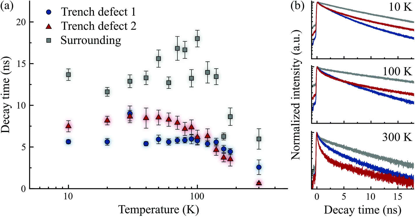 | ||
| Fig. 5 (a) Temperature dependence of the 1/e decay time of trench defect 1, trench defect 2 and the surrounding material, and (b) time decay curves (at peak emission energy) taken at 10 K, 100 K and 300 K. | ||
From Fig. 5(a) we can observe that in all 3 regions (surrounding, trench defect 1 and trench defect 2), the decay time is initially fairly constant with temperature but then decreases at higher temperatures. Such a decrease in lifetime is commonly associated with carrier recombination being increasingly dominated by non-radiative processes. We note that in the case of trench defect 1, the onset of this decrease occurs at higher temperatures (near 140 K) in comparison to trench defect 2 or the surrounding material (70–90 K), which may corroborate our earlier suggestion that strain relaxation of the enclosed QWs allows faster radiative recombination, which can therefore remain the dominant recombination mechanism up to higher temperatures. We could add here that carrier transport becomes activated as the temperature increases. Therefore, it is possible that the thin inclined sidewall QWs of the trench further helps reducing non-radiative recombination by repelling the carriers away from the non-radiative SMB. However, it is important to note that our power-dependent studies (Fig. 2) indicate that the dominant mechanisms for recombination at trench defects change with increasing probe current, so that the observed robustness of the emission to the presence of a local non-radiative centre, does not persist to higher probe current.
We finally note (in Fig. 5(b)) that throughout the temperature range, the time decay curves of trench defect 2 and surrounding material are parallel after a few nanoseconds (ca. 5 ns). This is a strong indication that the long-lived component of the transient in these two regions of the sample are similar, and is aligned with our observation that the CL emission from trench defects with a narrow trench is dominantly due to the QWs below the BSF which are similar to the surrounding QWs.
As a general observation we would like to point out that the structure of trench defects with a wide trench offers an interesting configuration for thermionic emission and recapture of carriers.46,47 The gradual indium composition change across the QW stack combined with the greater radiative recombination rate implies that thermal redistribution of carriers would populate preferentially the topmost QWs, which coincidentally are best separated from the influence of the non-radiative SMB, by the presence of the narrow sidewall QWs. This would be an example where defects could advantageously be used to engineer nanoscale light emitting structures.
Conclusions
In conclusion we investigated the carrier dynamics at trench defects in InGaN/GaN QWs by means of power-dependent CL and temperature-dependent time-resolved CL. The study confirms that the emission properties of trench defects closely relate to the position of the BSF in the QW stack. In particular trench defect with a wide trench have a BSF located at the bottom of the QW stack, and the emission properties are dictated by the dynamics of carriers in the enclosed region. On the other hand, trench defects with a narrow trench have a BSF located near the top of the QW stack, consequently the emission properties are hybrid between that of the enclosed region and that of the surrounding QWs. Our study of the time decay across the CL spectrum provides evidence that strain relaxation of the enclosed QWs result in the enhanced radiative recombination even in the presence of increased indium contents, explaining the peculiar luminescence properties of trench defects reported in previous literature.Author contributions
Conceptualization: GK, RAO, FM; data curation: GK, EC, KL; formal analysis: GK, SH, PD, RAO, FM; funding acquisition: RAO; methodology: GK, MK; supervision: RAO, FM; visualization: FM; writing – original draft: FM; writing – review & editing: GK, SH, PD, RAO, FM.Conflicts of interest
There are no conflicts to declare.Acknowledgements
This project is funded by the Engineering and Physical Sciences Research Council (EPSRC Grant No. EP/R025193/1). E. C. would like to acknowledge support from the Royal Microscopy Society Studentship. The authors are deeply saddened by the loss of Prof. Phil Dawson during the preparation of the manuscript, and would like to commemorate this close friend and colleague, who has made an enormous contribution to the optical study of semiconductors throughout his career.References
- S. Nakamura, Ann. Phys., 2015, 527, 335 CrossRef CAS.
- H. Amano, et al. , J. Phys. D: Appl. Phys., 2018, 51, 163001 CrossRef.
- T. Moustakas and R. Paiella, Rep. Prog. Phys., 2017, 80, 106501 CrossRef PubMed.
- B. Ding, Mater. Sci. Technol., 2018, 34, 1615 CrossRef CAS.
- F. C.-P. Massabuau, M. J. Davies, F. Oehler, S. K. Pamenter, E. J. Thrush, M. J. Kappers, A. Kovacs, T. Williams, M. A. Hopkins, C. J. Humphreys, P. Dawson, R. E. Dunin-Borkowski, J. Etheridge, D. W. E. Allsopp and R. A. Oliver, Appl. Phys. Lett., 2014, 105, 112110 CrossRef.
- S. Hammersley, M. J. Kappers, F. C.-P. Massabuau, S.-L. Sahonta, P. Dawson, R. A. Oliver and C. J. Humphreys, Appl. Phys. Lett., 2015, 107, 132106 CrossRef.
- T. Langer, H. Jonen, A. Kruse, H. Bremers, U. Rossow and A. Hangleiter, Appl. Phys. Lett., 2013, 103, 022108 CrossRef.
- F. C.-P. Massabuau, S.-L. Sahonta, L. Trinh-Xuan, S. Rhode, T. J. Puchtler, M. J. Kappers, C. J. Humphreys and R. A. Oliver, Appl. Phys. Lett., 2012, 101, 212107 CrossRef.
- F. C.-P. Massabuau, L. Trinh-Xuan, D. Lodie, E. J. Thrush, D. Zhu, F. Oehler, T. Zhu, M. J. Kappers, C. J. Humphreys and R. A. Oliver, J. Appl. Phys., 2013, 113, 073505 CrossRef.
- J. Bruckbauer, P. R. Edwards, T. Wang and R. W. Martin, Appl. Phys. Lett., 2011, 98, 141908 CrossRef.
- J. Bruckbauer, P. R. Edwards, S.-L. Sahonta, F. C.-P. Massabuau, M. J. Kappers, C. J. Humphreys, R. A. Oliver and R. W. Martin, J. Phys. D: Appl. Phys., 2014, 47, 135107 CrossRef.
- D. I. Florescu, S. M. Ting, J. C. Ramer, D. S. Lee, V. N. Merai, A. Parkeh, D. Lu, E. A. Armour and L. Chernyak, Appl. Phys. Lett., 2003, 83, 33 CrossRef CAS.
- M. Senthil Kumar, J. Y. Park, Y. S. Lee, S. J. Chung, C.-H. Hong and E.-K. Suh, J. Phys. D: Appl. Phys., 2007, 40, 5050 CrossRef.
- J. Smalc-Koziorowska, E. Grzanka, R. Czernecki, D. Schiavon and M. Leszczynski, Appl. Phys. Lett., 2015, 106, 101905 CrossRef.
- S. M. Ting, J. C. Ramer, D. I. Florescu, V. N. Merai, B. E. Albert, A. Parekh, D. S. Lee, D. Lu, D. V. Christini, L. Liu and E. A. Armour, J. Appl. Phys., 2003, 94, 1461 CrossRef CAS.
- M. Senthil Kumar, Y. S. Lee, J. Y. Park, S. J. Chung, C.-H. Hong and E.-K. Suh, Mater. Chem. Phys., 2009, 113, 192 CrossRef.
- S.-L. Sahonta, M. J. Kappers, D. Zhu, T. J. Puchtler, T. Zhu, S. E. Bennett, C. J. Humphreys and R. A. Oliver, Phys. Status Solidi A, 2013, 210, 195 CrossRef CAS.
- T. Hikosaka, T. Shioda, Y. Harada, K. Tachibana, N. Sugiyama and S. Nunoue, Phys. Status Solidi C, 2011, 8, 2016 CrossRef CAS.
- D. Iida, S. Lu, S. Hirahara, K. Niwa, S. Kamiyama and K. Ohkawa, J. Cryst. Growth, 2016, 448, 105 CrossRef CAS.
- F. C.-P. Massabuau, C. C. Tartan, R. Traynier, W. E. Blenkhorn, M. J. Kappers, P. Dawson, C. J. Humphreys and R. A. Oliver, J. Cryst. Growth, 2014, 386, 88 CrossRef CAS.
- F. C.-P. Massabuau, A. Le Fol, S. K. Pamenter, F. Oehler, M. J. Kappers, C. J. Humphreys and R. A. Oliver, Phys. Status Solidi A, 2014, 211, 740 CrossRef CAS.
- F. Massabuau, M. Kappers, C. Humphreys and R. Oliver, Phys. Status Solidi B, 2017, 254, 1600666 CrossRef.
- S. Suihkonen, T. Lang, O. Svensk, J. Sormunen, P. T. Torma, M. Sopanen, H. Lipsanen, M. A. Odnoblyudov and V. E. Bougrov, J. Cryst. Growth, 2007, 300, 324 CrossRef CAS.
- T. Suzuki, M. Kaga, K. Naniwae, T. Kitano, K. Hirano, T. Takeuchi, S. Kamiyama, M. Iwaya and I. Akasaki, Jpn. J. Appl. Phys., 2013, 52, 08JB27 CrossRef.
- S. L. Rhode, W. Y. Fu, M. A. Moram, F. C.-P. Massabuau, M. J. Kappers, C. McAleese, F. Oehler, C. J. Humphreys, R. O. Dunsane and S.-L. Sahonta, J. Appl. Phys., 2014, 116, 103513 CrossRef.
- F. C.-P. Massabuau, P. Chen, M. K. Horton, S. L. Rhode, C. X. Ren, T. J. O'Hanlon, A. Kovacs, M. J. Kappers, C. J. Humphreys, R. E. Dunin-Borkowski and R. A. Oliver, J. Appl. Phys., 2017, 121, 013104 CrossRef.
- E. Taylor, F. Fang, F. Oehler, P. R. Edwards, M. J. Kappers, K. Lorenz, E. Alves, C. McAleese, C. J. Humphreys and R. W. Martin, Semicond. Sci. Technol., 2013, 28, 065011 CrossRef.
- H. Wang, Z. Lv, S. Zhang, B. Li, Z. Wu and H. Jiang, Appl. Phys. Express, 2019, 12, 105502 CrossRef CAS.
- W. Liu, J.-F. Carlin, N. Grandjean, B. Deveaud and G. Jacopin, Appl. Phys. Lett., 2016, 109, 042101 CrossRef.
- F. C.-P. Massabuau, M. K. Horton, E. Pearce, S. Hammersley, P. Chen, M. S. Zielinski, T. F. K. Weatherley, G. Divitini, P. R. Edwards, M. J. Kappers, C. McAleese, M. A. Moram, C. J. Humphreys, P. Dawson and R. A. Oliver, J. Appl. Phys., 2019, 125, 165701 CrossRef.
- M. E. Vickers, M. J. Kappers, T. M. Smeeton, E. J. Thrush, J. S. Barnard and C. J. Humphreys, J. Appl. Phys., 2003, 94, 1565 CrossRef CAS.
- D. Drouin, P. Hovington and R. Gauvin, Scanning, 1997, 19, 20 CrossRef CAS.
- T. J. O'Hanlon, F. C.-P. Massabuau, A. Bao, M. J. Kappers and R. A. Oliver, Ultramicroscopy, 2021, 231, 113255 CrossRef PubMed.
- F. C.-P. Massabuau, L. Trinh-Xuan, D. Lodié, S.-L. Sahonta, S. Rhode, E. J. Thrush, F. Oehler, M. J. Kappers, C. J. Humphreys and R. A. Oliver, J. Phys.: Conf. Ser., 2013, 471, 012042 CrossRef CAS.
- J. E. Northrup, J. Neugebauer and L. T. Romano, Phys. Rev. Lett., 1996, 77, 103 CrossRef CAS PubMed.
- T. L. Song, J. Appl. Phys., 2005, 98, 084906 CrossRef.
- T. Shioda, M. Sugiyama, Y. Shimogaki and Y. Nakano, Phys. Status Solidi A, 2010, 207, 1375 CrossRef CAS.
- P. Dawson, S. Schulz, R. A. Oliver, M. J. Kappers and C. J. Humphreys, J. Appl. Phys., 2016, 119, 181505 CrossRef.
- S. Schulz, M. A. Caro, C. Coughlan and E. P. O'Reilly, Phys. Rev. B: Condens. Matter Mater. Phys., 2015, 91, 035439 CrossRef.
- A. Morel, P. Lefebvre, S. Kalliakos, T. Taliercio, T. Bretagnon and B. Gil, Phys. Rev. B: Condens. Matter Mater. Phys., 2003, 68, 045331 CrossRef.
- Y. Narukawa, Y. Kawakami, S. Fujita and S. Nakamura, Phys. Rev. B: Condens. Matter Mater. Phys., 1999, 59, 10283 CrossRef CAS.
- S. Birner, T. Zibold, T. Andlauer, T. Kubis, M. Sabathil, A. Trellakis and P. Vogl, IEEE Trans. Electron Devices, 2007, 54, 2137 CAS.
- T. Langer, H.-G. Pietscher, F. A. Ketzer, H. Jönen, H. Bremers, U. Rossow, D. Menzel and A. Hangleiter, Phys. Rev. B: Condens. Matter Mater. Phys., 2014, 90, 205302 CrossRef.
- L. Marona, D. Schiavon, M. Baranowski, R. Kudrawiec, I. Gorczyca, A. Kafar and P. Perlin, Sci. Rep., 2020, 10, 1235 CrossRef CAS PubMed.
- S. Schulz, D. P. Tanner, E. P. O'Reilly, M. A. Caro, D. Sutherland, M. J. Davies, P. Dawson, F. Tang, J. T. Griffiths, F. Oehler, M. J. Kappers, R. A. Oliver and C. J. Humphreys, Phys. Rev. B: Condens. Matter Mater. Phys., 2015, 92, 235419 CrossRef.
- S. Hammersley, M. J. Davies, P. Dawson, R. A. Oliver, M. J. Kappers and C. J. Humphreys, Phys. Status Solidi B, 2015, 252, 890 CrossRef CAS.
- P. Hurst, P. Dawson, S. A. Levetas, M. J. Godfrey, I. M. Watson and G. Duggan, Phys. Status Solidi B, 2001, 228, 137 CrossRef CAS.
Footnotes |
| † Electronic supplementary information (ESI) available. See DOI: 10.1039/d1nr06088k |
| ‡ Deceased. |
| This journal is © The Royal Society of Chemistry 2022 |