
 Open Access Article
 This Open Access Article is licensed under a Creative Commons Attribution-Non Commercial 3.0 Unported Licence
Low-temperature characteristics of magnesium fluoride based bipolar RRAM devices
Nayan C.
Das
 a,
Minjae
Kim
a,
Jarnardhanan R.
Rani
a,
Sung-Min
Hong
a and
Jae-Hyung
Jang
*b
a,
Minjae
Kim
a,
Jarnardhanan R.
Rani
a,
Sung-Min
Hong
a and
Jae-Hyung
Jang
*b
aSchool of Electrical Engineering and Computer Science, Gwangju Institute of Science and Technology, Gwangju, 61005, South Korea
bSchool of Energy Engineering, Korea Institute of Energy Technology, Naju 58330, South Korea. E-mail: jjang@kentech.ac.kr
First published on 21st February 2022
Abstract
This study investigates the temperature-independent switching characteristics of magnesium fluoride (MgFx) based bipolar resistive memory devices at temperatures ranging from 300 K down to 77 K. Filament type resistive switching at the interface of Ti/MgFx and the trap-controlled space charge limited conduction (SCLC) mechanism in the bulk MgFx layer are confirmed. The experimental results indicate that the operating environment and temperature critically control the resistive switching performance by varying the non-stoichiometry of the amorphous MgFx active layer and Ti/MgFx interface region. The gaseous atmosphere (open air or vacuum) affects device performances such as the electroforming process, on-state current, off-state current, on/off ratio, SET/RESET voltage and endurance of resistive-switching memory devices. After electroforming, the device performance is independent of temperature variation. The Ti/MgFx/Pt memory devices show promising data retention for >104 s in a vacuum at room temperature and 77 K with the DC endurance property for more than 150 cycles at 77 K. The devices have great potential for future temperature-independent electronic applications.
1. Introduction
Explosively growing cloud computing and big data applications demand high-performance data centers requiring more extensive and energy-efficient memory systems. Cryogenic operation of memory systems has shown tremendous performance improvements in terms of speed and energy efficiency.1 Non-volatile memory (NVM) is one of the critical limiting factors in designing electronic devices for cryogenic temperature and harsh environment applications (e.g. aerospace, deep space exploration). In deep space exploration, ionizing radiation and cryogenic temperatures are frequently encountered. Developing a reliable radiation-hardened NVM technology that performs well at cryogenic temperatures and vacuum is crucial.2,3Resistive switching random access memory (RRAM) devices are one of the emerging memory technologies. The resistance states of RRAM devices are programmed by the applied voltage/current. As materials properties change with the temperature, the ambient thermal fluctuations influence the programmed resistance states of the device and shift them to a thermodynamically stable condition. The ideal RRAM device performance should be temperature-independent, and the resistance states should be stable in thermal fluctuations.4 Moreover, as the device's size decreases, the effect of the gaseous atmosphere and temperature intensifies because of the large specific surface area. Thus, understanding the influence of the operating environment on the device performance is necessary to design RRAM devices.4
Although RRAM devices have recently been extensively studied, most studies were carried out at room temperature and ambient pressure. Several studies investigated the effects of the operating environment on RRAM devices’ performance by varying air, oxygen, and nitrogen partial pressure.4–6 A few studies on HfOx based RRAM devices and only one study on Cu doped silica-based RRAM devices have been carried out at cryogenic temperatures.2,3,7–11 Nevertheless, all of the studies failed to report the device's cycle variability and stability in a vacuum and at cryogenic temperatures. Moreover, except for the Shang et al. study, all the other studies required an electroforming process in open air at room temperature to activate the resistive switching properties before measuring the device performance at cryogenic temperatures.2,3,7–11 Even at room temperature, electroforming voltages as high as 8 V are required.2 No information is provided about the possibility of electroforming at cryogenic temperatures in the above studies. Other studies showed that it is impossible to perform the electroforming process in a vacuum for SiO2, Ta2O5, and HfO2-based devices.12–16
When TiN/Ti/HfOx/TiN,8 Er/HfOx/AlOx/Pt,9 ITO/HfOx/ITO,10 and Pt/HfOx/TiN2 devices were cooled down to different cryogenic temperatures, they exhibited the temperature-dependent Poole-Frenkel effect, trap-assisted tunnelling, metallic conduction in the low resistance state, and a combination of the nearest-neighbouring hopping and the variable range hopping conduction, respectively. The temperature-dependent conduction mechanisms exhibited by the above devices depend on the electrode/oxide or oxide/oxide bandgap offset and the trap density because electrons always seek the least resistive paths with the fastest transition rate.17
Even though the essential requirement for the ideal cryogenic temperature memory devices is a temperature-independent conduction mechanism, it has not been explored yet. These limitations, as mentioned earlier, need to be overcome to develop a reliable RRAM device that works in a vacuum at cryogenic temperatures. Thus, it is necessary to comprehensively study the interaction of the RRAM device with open air and vacuum with a temperature variation from room temperature to cryogenic temperatures.
Only RRAM devices based on two oxide materials (HfOx and silica) have been used for low-temperature studies to date. The operating environment and temperature heavily influence the properties of oxygen vacancy-based materials due to a large amount of oxygen available in the atmosphere. Thus, finding an alternative anion vacancy-based material that is less influenced by the operating environment is a way to overcome the limitations of oxygen vacancy-based RRAMs.
The biodegradable magnesium fluoride (MgFx) has been used in many eco-friendly electronic devices.18 MgFx is a wide bandgap (11.3 eV) insulator suitable for RRAM devices. Recently, a couple of reports on MgFx based RRAM devices have shown their resistive switching and biodegradable properties at room temperature and in open air.18,19 However, both the reported devices required an electroforming process to initiate the resistive switching properties. Moreover, the resistive switching mechanism and conduction mechanism in MgFx based RRAM devices are not fully understood. The effects of vacuum at cryogenic temperatures on the device performance have not been studied yet.
Our recent work shows the electroforming-free bipolar resistive switching behaviour of Ti/MgFx/Pt devices with the trap-controlled space charge limited current (SCLC) conduction mechanism in the atmospheric environment.20 The temperature-independent SCLC conduction mechanism makes the Ti/MgFx/Pt device a potential candidate for a reliable cryogenic memory device.21 Thus, it is crucial to investigate the cryogenic performance of MgFx based RRAM devices.
This work reports for the first time fluoride vacancy-based Ti/MgFx/Pt RRAM devices operable at cryogenic temperatures without pre-treatment in open air and at room temperature. They exhibit favourable resistive switching properties in air at room temperature and in a vacuum at temperatures ranging from 77 K to 300 K with promising retention and endurance properties. The operating environment influences the temperature-independent performance of Ti/MgFx/Pt RRAM devices. Depending on the operating environment, the availability of the weakly bonded hydroxyl groups influences the surface chemistry of the amorphous MgFx active layer and the Ti/MgFx interface, which subsequently changes the elemental composition of the Ti/MgFx interface region. Finally, mechanisms are presented in detail with a suitable conduction and resistive switching model.
2. Experimental
Ti/MgFx/Pt devices were fabricated with a 150 nm-thick Ti top electrode, 50 nm-thick MgFx, and 150 nm-thick Pt bottom electrode on a SiO2/Si substrate by electron beam (e-beam) evaporation at ambient substrate temperature. Circular-shaped shadow masks were used to pattern the variable size and thickness of MgFx and 150 nm-thick Ti top electrodes during e-beam evaporation at ambient substrate temperature. 50 nm-thick MgFx based devices with four different top electrode radii (25, 50, 150, and 225 μm) were fabricated to analyse the area dependency. To investigate the effect of the gaseous atmosphere (open air or vacuum) on the active layer, Fourier transform infrared (FTIR) absorbance spectroscopy was carried out on 1 μm-thick MgFx films grown separately on a SiO2/Si substrate.The electrical characteristics of the memory devices were measured using a semiconductor parameter analyser (HP-4155A). Voltage was applied directly to the top electrode while the bottom electrode was grounded. The electrical characteristics of RRAM devices in a vacuum environment and at cryogenic temperatures were measured using the MS-TECH Vacuum Chamber Probe Station (<10−5 torr).
3. Results and discussion
3.1. Properties of the MgFx film
The structural, elemental, and compositional properties of the MgFx thin film were analysed in detail by XRD, SEM, XPS analysis, and FTIR absorbance spectroscopy measurement in a previous study.20 The XRD and SEM analyses revealed that the defect-rich amorphous granular structured MgFx layer was successfully deposited by keeping the substrate temperature at ambient temperature during e-beam evaporation.22,23 XPS analysis shows that the Mg/F ratio in the as-deposited MgFx film is around 1![[thin space (1/6-em)]](https://www.rsc.org/images/entities/char_2009.gif) :1.65, which shows fluoride vacancies in the film with small amounts of oxygen.20
:1.65, which shows fluoride vacancies in the film with small amounts of oxygen.20
FTIR absorbance spectra for the MgFx thin film measured in open air and vacuum environments are shown in Fig. 1. The stable characteristic absorbance peak of the Mg–F bond is found at 613 cm−1 for both measurement conditions. However, many weak absorption peaks are observed between 3800–3500 cm−1 and 1700–1450 cm−1 associated with the weak binding between Mg2+ sites and different vibrational modes (stretching and bending) of hydroxyl groups under open-air measurement conditions.24–26 These hydroxyl groups indicate H2O was present on the surface of the amorphous MgFx that was absorbed from the atmosphere during the fabrication process.13,23,25 A weak CO2 vibration band is detected at around 2375–2385 cm−1.26 In a vacuum environment, all the weakly bonded hydroxyl groups and CO2 are easily removed from the surface of the amorphous MgFx thin film.25,27,28
 | ||
| Fig. 1 FTIR absorbance spectra of the MgFx thin film measured in open air and a vacuum environment. | ||
The presence and absence of these weakly bonded groups influence the surface properties of the amorphous MgFx active layer and the Ti/MgFx interface.13,16,29,30 Consequently, Ti/MgFx/Pt device performances are influenced by the operating environment.
3.2. Electrical characteristics of the Ti/MgFx/Pt device
The feasibility of the Ti/MgFx/Pt memory device at cryogenic temperatures is investigated in two steps. At first, the Ti/MgFx/Pt device performances (I–V measurement) are carried out in a vacuum chamber and at room temperature. Finally, the Ti/MgFx/Pt device performance is measured in the vacuum chamber at 77 K. | ||
| Fig. 2 (a) Typical I–V characteristics; (b) data retention and (c) endurance characteristics of the Ti/MgFx/Pt memory devices in a vacuum at room temperature. | ||
The device comes back to the new HRS when the negative voltage is applied. After electroforming, the sequence was changed to 0 V → + 3 V → 0 V → −3 V → 0 V. The resistance switching from the new HRS to the LRS occurs at around +1 V (VSET), lower than VFORM. Similarly, when a negative voltage is applied, the current starts decreasing from the LRS to the HRS at the RESET voltage (VRESET) around −2.5 V. The LRS current (ILRS) and HRS current (IHRS) values of the device were read at +0.50 V (VREAD).
The pristine Ti/MgFx/Pt device requires an electroforming process to activate resistive switching properties in the vacuum environment, which was not necessary when the devices are operated in open air at 300 K. Moreover, it exhibited the initial resistance (∼10 GΩ) much higher than that (∼10 MΩ) in open air at 300 K, where the device exhibited electroforming-free characteristics.20 In a vacuum, weakly bonded hydroxyl groups and CO2 are removed from the surface of the amorphous MgFx thin film, which makes the active layer more resistive, and the overall initial resistance of the Ti/MgFx/Pt device increases by a factor of 3.12–15,31 After electroforming, CF dissolves partially in a weak point of the CF during the RESET process, and the device reaches the new HRS, which is less resistive than the initial HRS. Further SET/RESET processes occur by reconstruction and partial breakdown of the CF, which needs a smaller magnitude of voltages (|VSET| and |VRESET|) than |VFORM|.32
The device shows promising data retention over 104 s with an on/off ratio of ∼10 in a vacuum at room temperature, as shown in Fig. 2(b). A total of 75 DC cyclic measurements were performed to confirm the stability of the resistance states in a vacuum at room temperature. The LRS shows a more stable and uniform cyclic property than the HRS (Fig. 2(c)).
3.2.1.1. Area dependency
Fig. 3 shows the area-dependent characteristics of Ti/MgFx/Pt devices in a vacuum. VFORM, VSET, and VRESET are independent of the device area (Fig. 3(a)). Both currents (ILRS and IHRS) show area independence (Fig. 3(b)). This area independent voltages (VFORM, VSET, and VRESET) and currents (ILRS and IHRS) indicate that the resistive switching in Ti/MgFx/Pt devices is filament type.33,34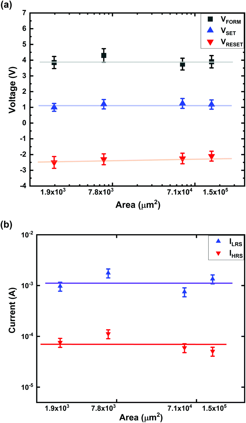 | ||
| Fig. 3 Electrical characteristics of Ti/MgFx/Pt devices having various areas. (a) VFORM, VSET, and VRESET; (b) ILRS and IHRS with respect to the device area. | ||
After the electroforming process, the current flows through the CF instead of the total device area in the LRS. After the RESET process, the current is dominated by thermally activated localized states at the partially dissolved CFs instead of the bulk layer.33–37
3.2.1.2. Thickness dependency
The performance parameters of Ti/MgFx/Pt memory devices having various active layer thicknesses are compared in Fig. 4. The electroforming characteristics of the devices with different active layer thicknesses are shown in Fig. 4(a). VFORM, VSET and VRESET are independent of the active layer thickness (Fig. 4(b)). ILRS does not show any thickness dependency, but IHRS decreases as the thickness increases (Fig. 4(c)). The thickness independent voltages (VFORM, VSET, and VRESET) and currents (ILRS) indicate that CFs are formed at the interface of Ti/MgFx instead of between two electrodes.38,39 The initial resistance increases and IHRS decreases with the thickness of the active layer because the charge carrier movement gets more difficult as the bandgap of the active layer increases with the thickness.40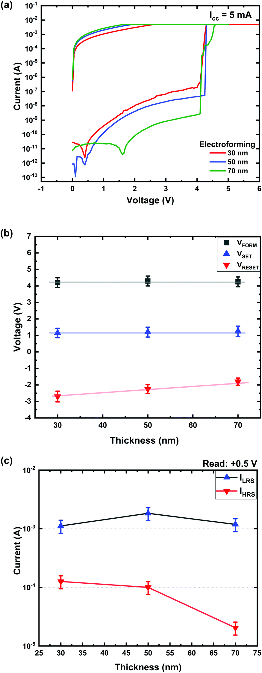 | ||
| Fig. 4 Performance of the Ti/MgFx/Pt memory devices having various active layer thicknesses. (a) Electroforming process, (b) VFORM, VSET, and VRESET (c) ILRS and IHRS with respect to the active layer thickness. | ||
When long CFs are formed between two electrodes through the active bulk layer, a higher electroforming voltage is needed for the thicker devices.41 However, the electroforming voltage is essentially the same (∼4 V) for all the Ti/MgFx/Pt memory devices having various MgFx thicknesses. The thickness independent VFORM, VSET, and VREST indicate that the voltage drop primarily occurs at the electrode/dielectric interface.42 Compared to the bulk, the thickness of the interface region is almost constant, and the resistive switching of the device occurs at a local CF rather than over the entire interfacial area.42–47
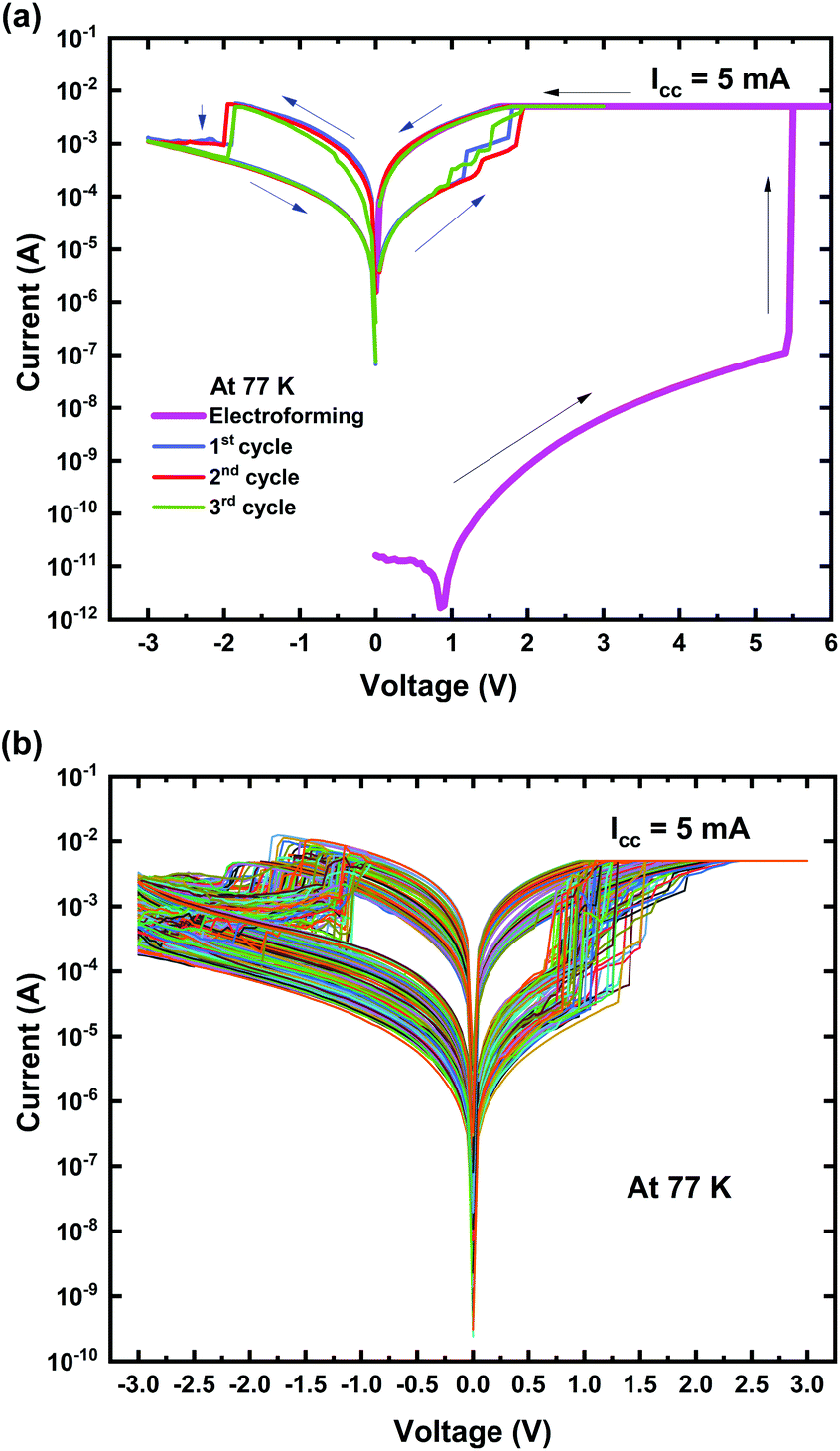 | ||
| Fig. 5 Ti/MgFx/Pt memory device performance at 77 K; (a) typical I–V characteristics with electroforming; (b) I–V characteristics of 200 cycles after electroforming. | ||
The pristine Ti/MgFx/Pt device is in the HRS at low temperature and exhibits a resistance of 100 GΩ that is much higher than the HRS resistance (∼10 GΩ) in a vacuum at room temperature. Electroforming occurs at VFORM around +5.5 V that is also higher than that in a vacuum at 300 K. The lower temperature makes the device more resistive, associated with a semiconducting behaviour, indicating that the thermionic conduction process is possibly involved. The construction and dissolution of the CF comprise charge transfer, ion motion, and nucleation. All of these processes must be affected by temperature.3 As the temperature is lowered to 77 K, the thermal energies of fluoride vacancies and ions are reduced. Consequently, the device needs a higher VFORM to form CFs.2,9 As a result, at low temperatures, an increase in the initial resistance and VFORM is observed.
After electroforming, the cycle sequence was changed to 0 V → + 3 V → 0 V → −3 V → 0 V. The SET and RESET process (VSET, VRESET, ILRS, and IHRS) follows the same pattern as in a vacuum at room temperature (300 K) (Fig. 5(a)). The device performed well at 77 K with a minimum on/off ratio >10 with 200 consecutive cycles, as shown in Fig. 5(b).
At 77 K, the variation in the I–V curves of the device performances results from different CF configurations at the Ti/MgFx interface consisting of traps with varying heights of the barrier by the different bias cycles.2
The data retention and endurance characteristics of Ti/MgFx/Pt memory devices in a vacuum at 77 K are shown in Fig. 6(a) and (b), respectively.
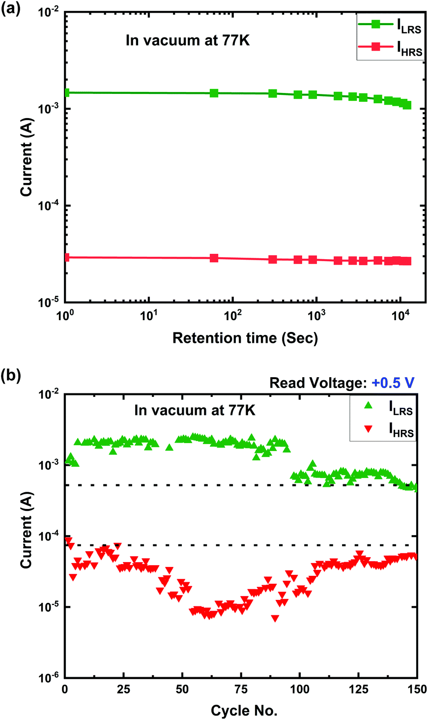 | ||
| Fig. 6 (a) Data retention and (b) endurance characteristics of the Ti/MgFx/Pt memory devices in a vacuum at 77 K. | ||
Fig. 6(a) shows that the device also performs promising data retention over 104 s with an on/off ratio higher than 10 in a vacuum at 77 K. In a vacuum at 77 K, 150 DC cyclic measurements were performed to confirm the stability of the resistance states (Fig. 6(b)). At 77 K also, the LRS shows a more uniform cyclic property than the HRS. Compared to that in a vacuum at room temperature, the device performs better in a vacuum at 77 K.
To investigate the effect of the temperature on the performance of the Ti/MgFx/Pt memory device, I–V characteristics are measured from 77 K to 300 K after electroforming at 77 K. In Fig. 7(a), the switching I–V curves are compared at temperatures ranging from 77 K to 300 K. VSET and VRESET as a function of temperature are presented in Fig. 7(b). The on and off currents of the devices with respect to temperature are shown in Fig. 7(c).
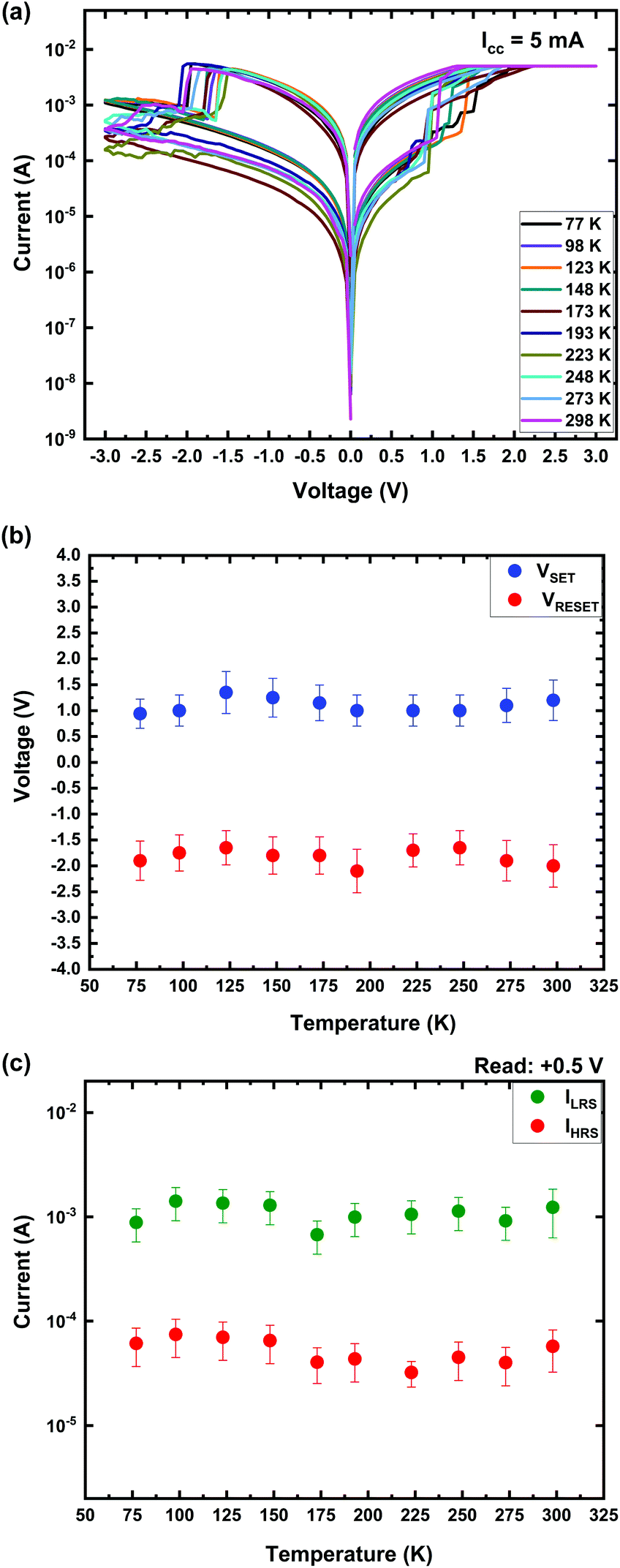 | ||
| Fig. 7 Ti/MgFx/Pt memory device performance with temperature variation from 77 K to 300 K. (a) Typical I–V curves vs. temperature; (b) VSET and VRESETvs. temperature; (c) ILRS and IHRSvs. temperature. | ||
As demonstrated in Fig. 7, after electroforming, the small variation in VSET, VRESET, ILRS, and IHRS implies essentially temperature-independent switching characteristics. The slight variation in VRESET and VSET indicates that the CFs are not entirely dissolved after RESET. A partially ruptured CF has been shown by atomic-level simulation.3,48 The CF rupture in the RESET process is attributed to the combined effects of the anion vacancy recombination by electric fields (primarily) and localized Joule heating (assisting).11,33,49,50 Joule heating can obscure the operating ambient temperature effect as the local temperature due to Joule heating can surpass the ambient temperature by a significant amount.50,51 Thus, after electroforming, the switching characteristics (VSET, VRESET, ILRS, and IHRS) of the Ti/MgFx/Pt memory device are not affected by the temperature variation. These temperature-independent characteristics are favourable for the stable operation in the appropriate temperature range, which is desirable for application of the RRAM technology.52 The above analyses show that the F vacancies play a significant role in forming the CF and resistive switching of Ti/MgFx/Pt memory devices.33,53–55 Nevertheless, Ti ions, which are smaller in size and have higher charge than fluoride ions, may contribute to the RS properties as mobile species. Thus further investigations are needed to clarify the role of Ti ions.
(I)–log(V) plot of the Ti/MgFx/Pt device is shown in Fig. 8 to explore the current conduction process at 77 K after electroforming. The positive voltage regions are divided into L1, L2, L3, L4, L5, and L6 (Fig. 8(a)). Similarly, the negative voltage regions are divided into LN1, LN2, LN3, LN4, and L5 (Fig. 8(b)).
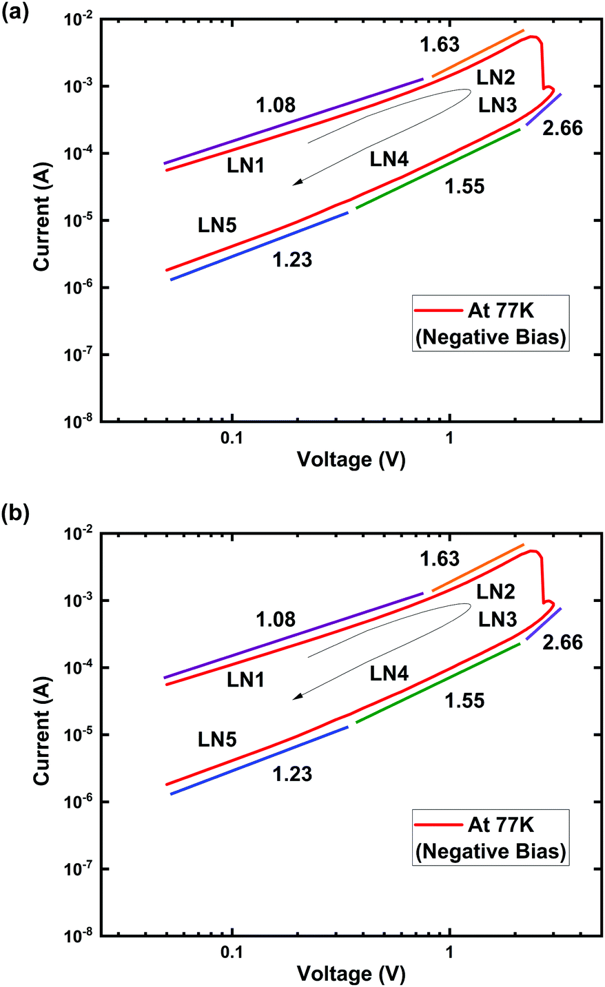 | ||
| Fig. 8 Log(I)–log(V) characteristics of Ti/MgFx/Pt memory devices with Icc = 5 mA at 77 K. (a) Positive bias voltage region; (b) negative bias voltage region. | ||
In the positive voltage region, the slope of the LRS (L6: 1.07) indicated ohmic conduction (I ∝ V) at low voltage. At higher voltages, the slopes of the HRS (L2: 1.98) and LRS (L5: 1.57) follow Child's law ((I ∝ Vn where n = 1.5–2.0). In the SET voltage region (L3: 30.29 and L4: 4.14), the conduction mechanism follows Child's law (I ∝ Vn where n = 4–30). The negative voltage region also shows a similar pattern. On the other hand, the current conduction mechanisms in the HRS are quite different. The slopes (L1: 1.38, LN5: 1.23) in the low voltage regions (L1 and LN5) are slightly higher than 1. It can be attributed to the incomplete fracture and formation of the CF during the RESET and SET process after electroforming at low temperatures. These analyses of the LRS and HRS indicate that the conducting behaviours are due to the trap-controlled space charge limited current (SCLC) conduction mechanism.21,56–59
The above analysis and previous study20 show that the conduction mechanism for the Ti/MgFx/Pt memory device is always the trap-controlled SCLC regardless of the operating environment and temperature.
The resistive switching mechanism with the step-by-step schematics of the Ti/MgFx/Pt memory device at cryogenic temperatures is proposed below (Fig. 9).
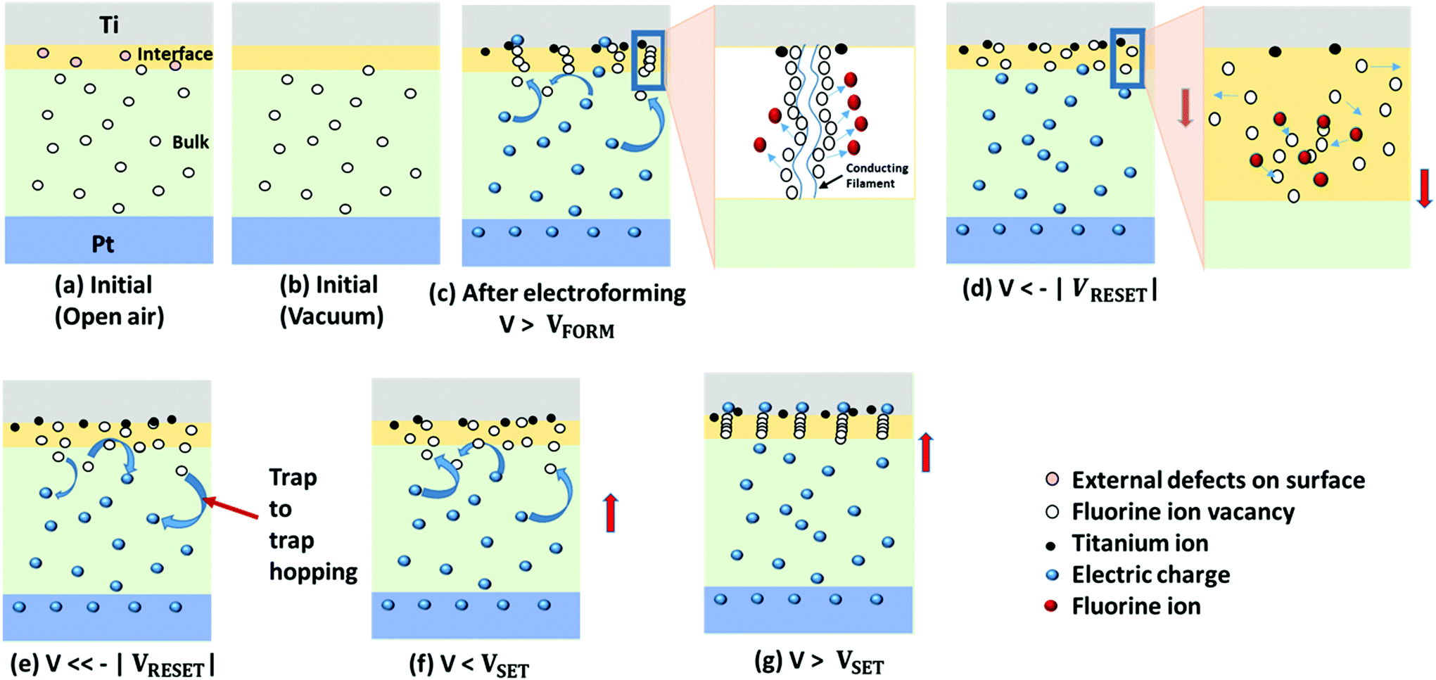 | ||
| Fig. 9 Schematics of the proposed switching mechanism of the Ti/MgFx/Pt memory device in a vacuum at 77 K. | ||
In open air at 300 K, pristine Ti/MgFx/Pt devices contain substantial internal defects (fluoride vacancies) in the bulk MgFx active layer. A small volume of weakly bonded O–H groups exists on the surface of MgFx in the form of external defects, facilitating the creation of anion vacancies at the interface by disassociating into differently charged species (O2− and H+). Thus, the presence of the ionic charge carriers in the interface region is altered from the bulk MgFx and increases the interface region's conductivity.16,29,30 All defects (internal and external) in Ti/MgFx/Pt devices are considered as traps (Fig. 9(a)).
However, weakly bonded O–H groups and CO2 are removed from the interface region in a vacuum. Thus, the ionic charge carriers (O2− and H+) are eliminated, and only the electronic current is present. Thus, the active layer becomes more resistive, and the overall initial resistance of the Ti/MgFx/Pt device increases.12–15,31 At low temperatures, the pristine device becomes more resistive due to the reduction of the thermal energies of ions and fluoride vacancies (Fig. 9(b)).2,9
Before reaching VFORM, under a positive applied voltage, electron injection is very weak. As a result, thermally generated free carriers largely dominate the conduction inside the MgFx film. As the voltage increases, the injected electron concentration becomes higher and exceeds the equilibrium electron concentration in the film, which governs the device's current conduction. When the voltage reaches near VFORM, the injected electrons are partly captured by the traps in the bulk MgFx film. Hence, conduction paths are created by the charge-trapping process from the bottom electrode to the interface through the traps in the bulk of the MgFx layer (Fig. 9(c)). The fluoride vacancies are localized at the interface rather than uniformly distributed, mainly formed at grain boundaries in the amorphous MgFx layer. Grain boundaries are the preferred conduction paths for fluoride vacancies, accumulating more smoothly at the electrode and changing the potential barrier at the electrode/oxide interfaces.18,30 Fluoride ions move from the grain boundaries to the top electrode (Ti) during the electroforming process. The forming and migrating energies of fluoride vacancies are around 1.44 eV and 0.85 eV, respectively, in MgFx.60 These values are lower than those of other RRAM-based oxygen vacancies.61 At VFORM, a localized CF is created by the fluoride vacancies in the interfacial region between the Ti and MgFx layers.38 In addition, the electrochemically oxidized Ti ions acting as donors can be injected at the Ti/MgFx interface under a high electric field and increase the conductivity. Thus, the device resistance state switches from the initial HRS to the LRS (in the inset figure of Fig. 9(c)).
When a negative voltage is applied for the RESET process, fluoride ions travel back to the CF and gradually recombine with the vacancies. At VRESET the CF at the interface is partially ruptured.62,63 Consequently, the interface region becomes resistive, and the overall device resistance state changes from the LRS to the new HRS (Fig. 9(d)). As the negative bias voltage further increases, electron de-trapping becomes evident. Conduction paths are reduced by the charge de-trapping process in bulk MgFx. The trapped electrons hop back through the fluoride-related traps of the MgFx layer from the interface to the bottom.19,59 As a result, the resistance state of the device switches to a new HRS, following the trap-controlled SCLC mechanism (Fig. 9(e)). The resistance of the new HRS is much lower than the initial HRS due to the partial breakdown of the CFs as a negative voltage (−3 V) is applied and only half of the voltage (+6 V) is used for the initial CF formation.
V SET is much lower than VFORM because the device is already in the new HRS with a partially fractured CF. As a result, when a positive voltage is applied, conduction paths are reconstructed by the charge trapping process through the fluoride vacancy-related electron traps in the bulk of MgFx (Fig. 9(f)). At VSET, a partially fractured CF is reformed with fluoride vacancies in the interfacial region between the Ti and MgFx layers. The resistance state of the device changes from the new HRS to the LRS (Fig. 9(g)).
4. Conclusions
A temperature-independent bipolar Ti/MgFx/Pt memory device was successfully fabricated, operating in a vacuum environment from ambient temperature (300 K) to low temperature (77 K).In a vacuum environment at 300 K, the device's initial resistance increases three orders of magnitude higher compared to that in the atmospheric environment. Thus, devices need an electroforming process to activate the resistive switching memory properties. The source of the device performance variation in the different operating environments is identified as the presence (in the atmospheric environment) and absence (in a vacuum) of a small amount of weakly bonded O–H groups at the interface of the top Ti electrode and the amorphous MgFx active layer. These O–H groups critically control the interface properties by providing additional charges.
In a vacuum environment at 77 K, the device shows a higher initial resistance and VFORM due to the decrease of the thermal energies of the charges compared to the vacuum environment at room temperature. At 77 K, the device shows promising stability and retention of >104 s with an on/off ratio higher than 10. After electroforming at 77 K, device operating parameters exhibit temperature-independent characteristics. These device characteristics are attributed to the fluoride vacancy-based filament type resistive switching at the Ti/MgFx interface and temperature-independent trap-controlled SCLC conduction mechanisms in the bulk MgFx layer, confirmed by the curve fitting analysis. The fluctuations in the device performances (VSET, VRESET, ILRS, and IHRS) are within a reasonable range and attributed to the cycle to cycle variability. Fully functional fluoride vacancy-based Ti/MgFx/Pt RRAM devices at cryogenic temperatures without being pre-conditioned in open air and temperature-independent properties after electroforming give the device superiority over existing devices. This study demonstrates that the Ti/MgFx/Pt memory device has great potential for deep space and cryogenic applications.
Author contributions
Conceptualization, N. C. D.; validation, M. J. K. and J. R. R.; writing—original draft preparation, N. C. D.; writing—review and editing, N. C. D., S.-M. H., and J.-H. J.; supervision, S.-M. H. and J.-H. J. All authors have read and agreed to the published version of the manuscript.Conflicts of interest
The authors declare no conflict of interest.Acknowledgements
This work was supported by 2017R1A2B3004049 and the Creative Materials Discovery Program (NRF-2017M3D1A1040828) through the National Research Foundation of Korea (NRF) funded by the Ministry of Science and ICT, Samsung Electronics grant, and KENTECH research grant (KRG2021-01-011).Notes and references
- Cryogenic Memory - Rambus, https://www.rambus.com/emerging-solutions/cryogenic-memory/, (accessed 3 May 2021).
- R. Fang, W. Chen, L. Gao, W. Yu and S. Yu, IEEE Electron Device Lett., 2015, 36, 567–569 CAS.
- W. Chen, N. Chamele, H. J. Barnaby and M. N. Kozicki, IEEE Electron Device Lett., 2017, 38, 1244–1247 CAS.
- K. Nagashima, T. Yanagida, K. Oka, M. Kanai, A. Klamchuen, S. Rahong, G. Meng, M. Horprathum, B. Xu, F. Zhuge, Y. He, B. H. Park and T. Kawai, Nano Lett., 2012, 12, 5684–5690 CrossRef CAS PubMed.
- L. Goux, P. Czarnecki, Y. Y. Chen, L. Pantisano, X. P. Wang, R. Degraeve, B. Govoreanu, M. Jurczak, D. J. Wouters and L. Altimime, Appl. Phys. Lett., 2010, 97, 243509 CrossRef.
- K. H. Chen, T. M. Tsai, C. M. Cheng, S. J. Huang, K. C. Chang, S. P. Liang and T. F. Young, Materials, 2018, 11, 43 CrossRef PubMed.
- M. Wang, C. Bi, L. Li, S. Long, Q. Liu, H. Lv, N. Lu, P. Sun and M. Liu, Nat. Commun., 2014, 5, 1–6 Search PubMed.
- C. Walczyk, D. Walczyk, T. Schroeder, T. Bertaud, M. Sowińska, M. Lukosius, M. Fraschke, D. Wolansky, B. Tillack, E. Miranda and C. Wenger, IEEE Trans. Electron Devices, 2011, 58, 3124–3131 CAS.
- C. Ahn, S. Kim, T. Gokmen, O. Dial, M. Ritter and H. S. P. Wong, Proc. Tech. Progr. - 2014 Int. Symp. VLSI Technol. Syst. Appl. VLSI-TSA 2014, 2014, pp. 1–2 Search PubMed.
- J. Shang, G. Liu, H. Yang, X. Zhu, X. Chen, H. Tan, B. Hu, L. Pan, W. Xue and R. W. Li, Adv. Funct. Mater., 2014, 24, 2171–2179 CrossRef CAS.
- P. Zhou, L. Ye, Q. Q. Sun, L. Chen, S. J. Ding, A. Q. Jiang and D. W. Zhang, IEEE Trans. Nanotechnol., 2012, 11, 1059–1062 Search PubMed.
- T. Tsuruoka, K. Terabe, T. Hasegawa, I. Valov, R. Waser and M. Aono, Adv. Funct. Mater., 2012, 22, 70–77 CrossRef CAS.
- I. Valov and T. Tsuruoka, J. Phys. D: Appl. Phys., 2018, 51, 413001 CrossRef.
- S. Tappertzhofen, M. Hempel, I. Valov and R. Waser, Mater. Res. Soc. Symp. Proc., 2011, 1330 DOI:10.1557/opl.2011.1198.
- S. Tappertzhofen, I. Valov, T. Tsuruoka, T. Hasegawa, R. Waser and M. Aono, ACS Nano, 2013, 7, 6396–6402 CrossRef CAS PubMed.
- M. Lübben, S. Wiefels, R. Waser and I. Valov, Adv. Electron. Mater., 2018, 4, 1–11 Search PubMed.
- S. Yu, X. Guan and H. S. P. Wong, Appl. Phys. Lett., 2011, 99, 16–19 Search PubMed.
- Z. Zhang, M. Tsang and I. W. Chen, Nanoscale, 2016, 8, 15048–15055 RSC.
- Y. Sun, C. Wang, H. Xu, B. Song, N. Li, Q. Li and S. Liu, AIP Adv., 2019, 9, 105117 CrossRef.
- N. C. Das, M. Kim, J. R. Rani, S.-M. Hong and J.-H. Jang, Micromachines, 2021, 12, 1049 CrossRef PubMed.
- E. W. Lim and R. Ismail, Electronics, 2015, 4, 586–613 CrossRef CAS.
- H.-H. Yang and G.-C. Park, Trans. Electr. Electron. Mater., 2010, 11, 33–36 CrossRef.
- T. Pilvi, T. Hatanpää, E. Puukilainen, K. Arstila, M. Bischoff, U. Kaiser, N. Kaiser, M. Leskelä and M. Ritala, J. Mater. Chem., 2007, 17, 5077–5083 RSC.
- S. Wuttke, A. Vimont, J. C. Lavalley, M. Daturi and E. Kemnitz, J. Phys. Chem. C, 2010, 114, 5113–5120 CrossRef CAS.
- L. Dumas, E. Quesnel, J.-Y. Robic and Y. Pauleau, J. Vac. Sci. Technol., A, 2000, 18, 465–469 CrossRef CAS.
- N. C. S. Selvam, R. T. Kumar, L. J. Kennedy and J. J. Vijaya, J. Alloys Compd., 2011, 509, 9809–9815 CrossRef CAS.
- K. Kinosita and M. Nishibori, J. Vac. Sci. Technol., 1969, 6, 730–733 CrossRef CAS.
- B. J. Sealy, A. J. Crocker, M. J. Lee and R. F. Egerton, Thin Solid Films, 1972, 11, 365–376 CrossRef CAS.
- R. Gao, D. Lei, Z. He, Y. Chen, Y. Huang, Y. En, X. Xu and F. Zhang, IEEE Electron Device Lett., 2020, 41, 38–41 Search PubMed.
- S. Bagdzevicius, K. Maas, M. Boudard and M. Burriel, J. Electroceram., 2017, 39, 157–184 CrossRef CAS.
- M. Lübben, S. Wiefels, R. Waser and I. Valov, Adv. Electron. Mater., 2018, 4(1), 1–11 Search PubMed.
- F. Zahoor, T. Z. Azni Zulkifli and F. A. Khanday, Nanoscale Res. Lett., 2020, 15(1) DOI:10.1186/s11671-020-03299-9.
- K. Santosh, in Nanoscale Semiconductor Memories, CRC Press, 2017 Search PubMed.
- D. Ielmini, S. Spiga, F. Nardi, C. Cagli, A. Lamperti, E. Cianci and M. Fanciulli, J. Appl. Phys., 2011, 109, 034506 CrossRef.
- Y. Lu, J. H. Lee, X. Yang and I. W. Chen, Nanoscale, 2016, 8, 18113–18120 RSC.
- Y. L. Song, Y. Liu, Y. L. Wang, M. Wang, X. P. Tian, L. M. Yang and Y. Y. Lin, IEEE Electron Device Lett., 2011, 32, 1439–1441 CAS.
- Y. Lu, J. H. Lee and I. W. Chen, Nanoscale, 2017, 9, 12690–12697 RSC.
- B. Traore, P. Blaise, B. Sklenard, E. Vianello, B. Magyari-Kope and Y. Nishi, IEEE Trans. Electron Devices, 2018, 65, 507–513 CAS.
- Y. J. Chen, H. L. Chen, T. F. Young, T. C. Chang, T. M. Tsai, K. C. Chang, R. Zhang, K. H. Chen, J. C. Lou, T. J. Chu, J. H. Chen, D. H. Bao and S. M. Sze, Nanoscale Res. Lett., 2014, 9, 1–5 CrossRef PubMed.
- L. P. Wang, P. De Han, Z. X. Zhang, C. L. Zhang and B. S. Xu, Comput. Mater. Sci., 2013, 77, 281–285 CrossRef CAS.
- F. M. Simanjuntak, D. Panda, K. H. Wei and T. Y. Tseng, Nanoscale Res. Lett., 2016, 11(1) DOI:10.1186/s11671-016-1570-y.
- M. Janousch, G. I. Meijer, U. Staub, B. Delley, S. E. Karg and B. P. Andreasson, Adv. Mater., 2007, 19, 2232–2235 CrossRef CAS.
- C. Schindler, G. Staikov and R. Waser, Appl. Phys. Lett., 2009, 94, 2007–2010 CrossRef.
- I. H. Inoue, S. Yasuda, H. Akinaga and H. Takagi, Phys. Rev. B: Condens. Matter Mater. Phys., 2008, 77, 1–7 Search PubMed.
- Y. P. Zhang, H. Wang, J. W. Xu, L. Yang, W. Qiu and Z. Da Li, Indian J. Eng. Mater. Sci., 2014, 21, 563–566 CAS.
- Y. C. Yang, F. Pan and F. Zeng, New J. Phys., 2010, 12, 023008 CrossRef.
- J. J. Yang, M. D. Pickett, X. Li, D. A. A. Ohlberg, D. R. Stewart and R. S. Williams, Nat. Nanotechnol., 2008, 3, 429–433 CrossRef CAS PubMed.
- N. Onofrio, D. Guzman and A. Strachan, Nat. Mater., 2015, 14, 440–446 CrossRef CAS PubMed.
- K. Jung, H. Seo, Y. Kim, H. Im, J. P. Hong, J. W. Park and J. K. Lee, Appl. Phys. Lett., 2007, 90, 1–3 Search PubMed.
- M. Uenuma, Y. Ishikawa and Y. Uraoka, Appl. Phys. Lett., 2015, 107, 073503 CrossRef.
- A. B. Chen, Doctoral dissertation, University of Pennsylvania, 2011 Search PubMed.
- E. Pérez, C. Wenger, A. Grossi, C. Zambelli, P. Olivo and R. Roelofs, J. Vac. Sci. Technol., B: Nanotechnol. Microelectron.: Mater., Process., Meas., Phenom., 2017, 35, 01A103 Search PubMed.
- B. Sundqvist and V. K. Tolpygo, J. Phys. Chem. Solids, 2018, 122, 41–50 CrossRef CAS.
- G. Dyos, The Handbook of Electrical Resistivity The Handbook of Electrical Resistivity, 2012 Search PubMed.
- G. K. White and S. B. Woods, Philos. Trans. R. Soc. London, Ser. A, 1959, 251 DOI:10.1098/rsta.1959.0004.
- F. C. Chiu, Adv. Mater. Sci. Eng., 2014, 2014, 578168 Search PubMed.
- Y. T. Li, S. B. Long, Q. Liu, H. B. Lü, S. Liu and M. Liu, Chin. Sci. Bull., 2011, 56, 3072–3078 CrossRef.
- F. C. Chiu, H. W. Chou and J. Y. M. Lee, J. Appl. Phys., 2005, 97, 103503 CrossRef.
- N. C. Das, S. I. Oh, J. R. Rani, S. M. Hong and J. H. Jang, Appl. Sci., 2020, 10, 3506 CrossRef CAS.
- D. S. Park and A. S. Nowick, J. Phys. Chem. Solids, 1976, 37, 607–617 CrossRef CAS.
- B. R. Field and D. Ielmini, IEEE Trans. Electron Devices, 2011, 58, 1–9 Search PubMed.
- X. C. Yuan, J. L. Tang, H. Z. Zeng and X. H. Wei, Nanoscale Res. Lett., 2014, 9, 1–5 CrossRef PubMed.
- C. Y. Lin, C. Y. Wu, C. Y. Wu, T. Y. Tseng and C. Hu, J. Appl. Phys., 2007, 102, 094101 CrossRef.
| This journal is © The Royal Society of Chemistry 2022 |