
Three-dimensional artificial chirality towards low-cost and ultra-sensitive enantioselective sensing
Yeseul
Kim†
 a,
Hongyoon
Kim†
a,
Younghwan
Yang†
a,
Trevon
Badloe
a,
Nara
Jeon
a and
Junsuk
Rho
*abc
a,
Hongyoon
Kim†
a,
Younghwan
Yang†
a,
Trevon
Badloe
a,
Nara
Jeon
a and
Junsuk
Rho
*abc
aDepartment of Mechanical Engineering, Pohang University of Science and Technology (POSTECH), Pohang 37673, Republic of Korea. E-mail: jsrho@postech.ac.kr
bDepartment of Chemical Engineering, Pohang University of Science and Technology (POSTECH), Pohang 37673, Republic of Korea
cPOSCO-POSTECH-RIST Convergence Research Center for Flat Optics and Metaphotonics, Pohang 37673, Republic of Korea
First published on 29th November 2021
Abstract
Artificial chiral structures have potential applications in the field of enantioselective signal sensing. Advanced nanofabrication methods enable a large diversity in geometric structures and broad selectivity of materials, which can be exploited to manufacture artificial three-dimensional chiral structures. Various chiroptical phenomena exploiting spin and orbital angular momentum at the nanoscale have been continuously exploited as a way to effectively detect enantiomers. This review introduces precisely controlled bottom-up and large-area top-down metamaterial fabrication methods to solve the limitations of high manufacturing cost and low production speed. Particle synthesis, self-assembly, glanced angled vapor deposition, and three-dimensional plasmonic nanostructure printing are introduced. Furthermore, emerging sensitive chiral sensing methods such as cavity-enhanced chirality, photothermal circular dichroism, and helical dichroism of single particles are discussed. The continuous progress of nanofabrication technology presents the strong potential for developing artificial chiral structures for applications in biomedical, pharmaceutical, nanophotonic systems.
 Yeseul Kim | Yeseul Kim obtained her B.S. (2020) in Materials Science and Engineering from Pohang University of Science and Technology (POSTECH). Currently, she is an M.S./Ph.D. student in Mechanical Engineering at POSTECH. Her research is mainly focused on quantum photonics and flat optics based on metasurfaces. She is a recipient of the Hyundai Motor Chung Mong-Koo fellowship and the POSTECHIAN fellowship. |
 Hongyoon Kim | Hongyoon Kim received his B.S. degree in Mechanical Engineering from POSTECH (2021). Currently, he is an M.S./Ph.D. student in Mechanical Engineering with POSTECH. He is a recipient of the POSTECH alchemist fellowship. His research interests include nanophotonics, metasurfaces, and AR/VR. |
 Younghwan Yang | Younghwan Yang received his B.S. degree in Mechanical Engineering from Ajou University (2018). Currently, he is an M.S./Ph.D. student in Mechanical Engineering at POSTECH. He is a recipient of the Hyundai Motor Chung Mong-Koo fellowship and the NRF Ph.D. candidate fellowship. |
 Trevon Badloe | Trevon Badloe obtained his M.Phys. (hons) degree from the University of Sheffield (2012) with one-year study abroad at National University of Singapore (2010). Currently, he is a Ph.D. student in Mechanical Engineering at POSTECH. His interests include tunable metamaterials and metasurfaces, and machine learning for the design and optimization of nanophotonic applications. |
 Nara Jeon | Nara Jeon received her B.S. degree in Chemical Engineering and Materials Science from Ewha Womans University (2022). Currently, she is an M.S./Ph.D. student in Mechanical Engineering at POSTECH. She is interested in tunable metasurfaces and nano-imprinting. |
 Junsuk Rho | Junsuk Rho is a Mu-Eun-Jae endowed chair associate professor with a joint appointment in the Department of Mechanical Engineering and the Department of Chemical Engineering at POSTECH. He received his degree his B.S. (2007) and M.S. (2008) in Mechanical Engineering at Seoul National University and the University of Illinois, Urbana-Champaign, respectively. After getting PhD (2013) in Mechanical Engineering and Nanoscale Science & Engineering from the University of California Berkeley, he had worked as a postdoctoral fellow in Materials Sciences Division at Lawrence Berkeley National Laboratory and the Ugo Fano fellow in Nanoscience and Technology Division at Argonne National Laboratory. |
Introduction
Chirality, a property defined as a system of objects that cannot be superimposed onto its mirror image, has been actively investigated at optical wavelengths from ultra-violet to infrared to distinguish chemical enantiomers for various tests in medicine and chemistry.1–5 Therefore, strong chiroptical responses are essential in both scientific research and industrial fields. Some well-known chiroptical responses are circular dichroism (CD: difference in absorption of left-circularly polarized light (LCP) and right-circularly polarized light (RCP)), optical rotatory dispersion (ORD: rotational degree of linear polarization), and helical dichroism (HD: the difference between oppositely-signed topological charges of a vortex beam).6–8For effectively distinguishing chiral molecular media, the field of metamaterials have been intensively researched to amplify weak intrinsic chiroptical signal. Among them, there are two types of metasurfaces that can be applied to chiral sensing which is achiral and chiral nanostructures.9,10 Achiral metamaterials have an advantage that they can suppress photothermal effect caused by the resonant of metallic structures, so they can detect chiral signals without the disturbance in temperature variation, which is important in distinguishing the chirality of low-thermal-resistant proteins. However, chiral nanostructure supports a stronger chiral near field than achiral nanostructures, so it can amplify weak chiral signals more than achiral structures.11 Therefore, artificial chirality from chiral metamaterials and plasmonic particles has been widely investigated to obtain sensitive chiroptical responses for use in practical enantioselective sensing devices. Additionally, for the fabrication of three-dimensional (3D) plasmonic chiral metamaterials, several fabrication methods including direct laser writing12–15 and focused-ion beam deposition16 have been investigated. However, both methods pattern nanostructure sequentially, hence they require a lot of time to fabricate large-area nanopatterns.
To solve these limitations of the expansive fabrication process and the sensitivity of its applications, mass-production techniques for complex chirality and various sensing methods have been investigated. Bottom-up synthesis enables massive production, but it generally could not fabricate symmetric broken structures at the nanoscale. Recently, advanced chiral synthesis such as peptide-assisted bottom-up,4 glanced-angled vapor deposition, and aerosol 3D printing methods reduced the fabrication cost. For the higher sensitivity in chiral sensing, scattering of spin angular momentum (SAM) and orbital angular momentum (OAM),6,17 as well as a photothermal effect,18,19 have been evaluated. For example, a nanoscale cavity can strongly confine electromagnetic fields and can amplify chiroptical responses,20 while the photothermal effect of chiral structures can be used to detect the chiral signals of individual chiral molecules.18
Here, in this mini-review, we present the progress of 3D chiral metamaterials in three emerging fields: Part (1) precise bottom-up synthesis with self-assembly, Part (2) large-area chiral structure fabrication based on physical vapor deposition, and Part (3) enhanced chiroptical responses with CD, photothermal effect, and HD. Part 1 and 2 focus on recent fabrication methods for low-cost massive artificial chiral structures, and part 3 shows practical sensing methods based on 3D chiral structures. In part 1, chiral particle synthesis methods and chiral-arrangement with gold nanorods are introduced, and in part 2, large-area chiral manufacturing based on physical vapor deposition is introduced. Finally, recent enantioselective sensing methods with 3D chiral structures have been introduced in part 3. We believe that bottom-up particle synthesis and large-area fabrication methods will enable the inexpensive fabrication of chiroptical sensing devices. In addition, enhanced chiroptical responses with OAM and photothermal effects obtain extremely high sensitivity in chiral sensors. Compared to the previous reviews, which focus on design and fabrication methods,2,3 theoretical modelling,1 or tunability of chiral metamaterials,21,22 this mini review will guide the next step of artificial chiroptical application research by covering both low-cost fabrications with sensitive chiral signal measurement methods.
Part 1. 3D self-assembly for fabrication of chiral metamaterials
Self-assembly is a process by which natural reactions spontaneously yield organized structures and is commonly used to fabricate 3D materials. It has been applied to synthesize 3D chiral metamaterials by exploiting physicochemical interactions between chemical components. In this paper, we will use the term ‘3D self-assembly’ as describing the method to create individually dispersed 3D chiral materials with complex shapes through self-assembly. The fabrication of arbitrary complex structures can be achieved with lower costs and higher precision than conventional top-down fabrication methods.23,24 Since 3D self-assembly methods are very diverse, it is difficult to understand everything through a short paper, but we will try to explain 3D self-assembly that makes chiral particles through a representative case. In this section, we introduce four examples of 3D self-assembly fabrication methods for chiral metamaterials. The first two cases in which the construction block contains metallic particles, and the other two methods are cases in which the construction block does not contain metallic components.The synthesis of plasmonic nanoparticles with chiral morphologies23,25–28 is a typical use of bottom-up self-assembly methods, which involves one or two seed-mediated aqueous chemical-reaction procedures.29 When amino acids and peptides interact enantioselectively with surfaces that have high Miller indices, the atoms tend to arrange on the surfaces with chiral characteristics during growth. The use of a chiral additive such as L-cysteine or D-cysteine has been used to manipulate the handedness of the resulting nanoparticles (Fig. 1a-i, ii).30 Because of the chiral geometry, the distributions of the electric field and magnetic field differ distinctly depending on the handedness of the incident circularly polarized light (Fig. 1a-iii). The chiral geometry of the final structures strongly affects the handedness-dependent CD signals (Fig. 1a-iv). Appropriate control of the growth kinetics by changing the concentration and injection time of the seed nanoparticles can affect the crystallographic and geometric characteristics of the resulting particles (Fig. 1a-v).31
 | ||
| Fig. 1 3D assembly of chiral metamaterials. (a) Chiral plasmonic nanoparticles.30,31 SEM images of the resulting particles (i) when L-cysteine is used as an additive, (ii) when D-cysteine is used as an additive.30 (iii) Electric and magnetic field distributions difference maps depending on circular polarization of incident light.30 (iv) CD spectra.30 (v) Schematic of morphology change depending on synthesis conditions.31 (b) Self-assembly with DNA origami.24 (i) Four pairs of plasmonic diastereomers (ii) Schematic of assembly process to fabricate diastereomers with two chiral centers. (iii) Results of agarose gel electrophoresis. (iv) TEM image of AuNR trimers. (v) CD spectra of four kinds of plasmonic diastereomers. (c) Block copolymer self-assembly.42 (i) Schematic of three synthetic types to fabricate different morphologies. TEM images of (ii) coil-like non-chiral helix and (iii) right-handed chiral helix. (iv) SEM and TEM images of morphology changes depending on thermal annealing. (d) Self-assembly of cellulose nanocrystals.47 (i) Schematic of synthesis process from CNCs to CNC-elastomer composites. (ii) SEM image of CNC-elastomer film. (iii) Fingerprint texture of stretched and relaxed condition. Polar plots of light intensities of (iv) relaxed, and (v) stretched cases. (vi) Birefringence vs stretching elongation. (a-ii, iii, and iv) Reproduction with permission from Ref. 42. (a-v) Reproduction with permission from 31. (b) Reproduction with permission from Ref. 42. (c) Reproduction with permission from Ref. 47. | ||
DNA can be programmed by sequence-dependent recognition and conformation, by which the position of long single-stranded DNA (ssDNA), called a “scaffold”, can be determined in connection with a short guiding ssDNA, called a “staple”.32 The DNA origami technique exploits the 3D self-assembly of ssDNA. Nano-architectures with chiral morphologies using DNA origami have been demonstrated as high-tech bottom-up fabrication as a way to easily yield arbitrary and dynamic nanostructures.24,32–34 Complex structures such as chiral molecules with multiple chiral centers have also been fabricated using the DNA origami method (Fig. 1b).24 With precursors with two chiral centers, four pairs of plasmonic diastereomers can be formed by self-assembly (Fig. 1b-i). The structure is composed of a scaffold, a staple, and gold nanorods (AuNRs), which are fixed through hybridization with DNA. An AuNR trimer is a structure with two chiral centers which can be produced by mixing and annealing processes using one precursor with a chiral center, called the ‘AuNR dimer’ and one with an incomplete chiral center, called the ‘free AuNR’ (Fig. 1b-ii). The success of self-assembly can be confirmed by comparing gel electrophoresis results before (Fig. 1b-iii, lane 1) and after (Fig. 1b-iii, lane 2) synthesis, and by examining TEM images (Fig. 1b-iv). Different diastereomeric shapes exhibit different CD properties (Fig. 1b-v). Four combinations of left-handed (L) and right-handed (R) are obtained. LL shows strong CD signals that are opposite to those of RR. LR and RL include a plane of symmetry, so the CD signal is weak.
Block copolymers composed of more than one species of monomer linked by chemical bonds have also been used as chiral assemblies.35 The morphologies of block copolymers depend on the thermal equilibrium condition with respect to the volume fraction of monomer blocks. Thus, various morphologies, such as lamellae and cylinders, and even chiral geometries, like gyroid,36,37 spiral,38–40 toroid,41 and helix, can be obtained by exploiting phase separation and reconstructions of block copolymers. For example (Fig. 1c),42 kinetic factors affect the morphologies of self-assembled block copolymers polystyrene-block-poly(D-lactide); three types of resulting morphologies can be obtained (Fig. 1c-i). The height h of the aqueous phase and the interfacial area S between aqueous phase and air determine the solvent evaporation rate Revap, which affects the assembly kinetics. When the particles are synthesized under condition I (high h and high S) to form coil-like chiral particle (morphology I), 78% of the particles have no chiral properties because the helix is randomly twisted (Fig. 1c-ii), whereas 22% of the particles are constantly twisted in the right-handed direction (Fig. 1c-iii), and thus chiral properties can be observed. As Revap is reduced using thermal annealing by raising the temperature to about 70 °C, the shape of the block copolymer particles gradually changed from the coil-like particles (morphology I) and the loop-like particles (morphology II) to the internal network structures (morphology III) (Fig. 1c-iv).
Cellulose is an abundant organic polymer.43 When it consists of both crystalline and amorphous domains, cellulose nanocrystals (CNCs) can be isolated by using acid to hydrolyze the amorphous domains and leave only the crystalline parts. CNCs can spontaneously organize to form a helical assembly, which induces selective optical reaction with respect to the handedness of light.44–46 A structure composed of spiral CNCs and elastomers has been suggested to obtain chiral particles (Fig. 1d).47 The spiral CNC is formed by an evaporation-induced self-assembly process (Fig. 1d-i). Initially, CNC and glucose particles are suspended in water and as it evaporates, the CNCs self-assemble into a left-handed spiral structure. At this time, the glucose particles help the CNC to expand uniformly without cracking during the subsequent drying process. When the resulting CNC-elastomer polymer is stretched, the chiral nematic part of the CNC unwinds and changes to a pseudo-nematic arrangement. When the polymer is extended to > 900%, the CNC changes from chiral to periodic (Fig. 1d-ii), and the difference in fingerprint textures between static and stretched CNC can be observed using polarized optical microscopy (Fig. 1d-iii). In polarized ultraviolet-visible spectroscopy measurements, the visible transmittance of the static CNC-elastomer composites is the same in all orientations (Fig. 1d-iv); this result indicates optical anisotropy. However, stretched samples are highly anisotropic because the optical axis is aligned along the stretching direction (Fig. 1d-v), so the birefringence increases in proportion to the elongation (Fig. 1d-vi).
In summary, this part introduced a method for fabricating individually dispersed, complex-shaped chiral structures. If the seed particles are achiral and metallic, the plasmonic chiral structures can be obtained by the growing process through chemical reactions, or stacking can be done using a DNA scaffold and staple. The block copolymers can controll their morphologies by using separation and reconstructions. We can make a chiral structure by stacking organic molecules like CNC to have specific handedness. As nano- or micro-level control technology develops, 3D self-assembly processes will become broader.
Part 2. Large-area 3D nanofabrication based on a physical vapor deposition
Practical nanophotonic applications such as enantioselective sensors48 require low-cost and large-area fabrication of 3D chiral metamaterials.2,49 However, at the nanoscale, symmetry-broken structures generally have higher surface energy than highly symmetric ones have. Therefore, chiral structures are difficult to fabricate using commercial bottom-up methods. This problem has been overcome by using glanced angled deposition (GLAD), twisted-layered stacking, and 3D aerosol printing methods. All three nanofabrication methods exploit physical vapor deposition that brings low step coverage. GLAD utilize one side film deposition on nanocone arrays; twisted stacking exploits Moiré patterns with two layers, which fabricate with physical vapor deposition of gold on polymer arrays; 3D aerosol printing uses a charged aerosol particle deposition with an array of hole mask that floats over a biased substrate. In this chapter, we introduce various methods for large-area fabrication of artificial 3D chiral structures that work in the visible and infrared regimes.GLAD has been used to fabricate free-standing nanocone-array metamaterials, which have been applied to chiral sensing50,51 (Fig. 2a). To fabricate free-standing chiral structure, a reactive-ion etching (RIE) process has been conducted on a polymer sphere array on a photoresist coated substrate to achieve an array of 600-nm-tall nanocones (Fig. 2a-i). Then GLAD was conducted to fabricate symmetric broken nanostructures. The tall structures enable a strong chiroptical response from ultra-violet to visible frequencies (Fig. 2a-ii). In measurements, a maximum CD intensity of −1.8° at wavelength λ = 800 nm is obtained (Fig. 2a-ii). These methods can be applied to self-assembled dielectric microsphere arrays,50–54 and low-temperature block-copolymer seeds.55
 | ||
| Fig. 2 Low-cost, large-area fabrication methods for 3D-chiral metamaterials. (a) Fabrication and optical responses of wafer-scale hollow nanocone array metamaterials.50 (i) Schematic of fabrication methods of nanocone array. Θ: angle between projection of metal deposition and perpendicular direction of a substrate. (ii) Top row: SEM images of fabricated samples with a height/diameter of 600/400, 350/200, 250/150 nm, respectively. Inset: 45° tilted view SEM images. Bottom row: measured g-factor at each fabricated sample. (b) Moiré chiral metamaterials.56 (i) Steps to fabricate Moiré chiral metamaterial by combining nanosphere lithography (NSL) and reactive ion-etching (RIE). (ii) Handedness of Moiré chiral metamaterials depend on the sign of twist angle ΘT between adjacent gold-hole-patterned layers. (iii) Measured and simulated chiroptical responses. The spectrum of CD is affected by ΘT. (c) Fabrication of plasmonic metamaterials by 3D aerosol printing.58 (i) Schematic of 3D aerosol printing that consist of piezo nanostage and SiNx mask. The SiNx mask focus charged aerosol particle at a small spot on a substrate. (ii) Various 3D plasmonic structures are fabricated by varying a relative position between a tip of structures and the mask hole. (iii) Structures can be predicted using aerosol simulation. (iv) SEM images of fabricated artificial chiral structures using the 3D aerosol printing. (a) Reproduction with permission from Ref. 50. (b) Reproduction with permission from Ref. 56. Reproduction with permission from Ref. 58. | ||
In a demonstration of creating chiral structures by stacking achiral structures, a twisted-layered achiral gold nanohole array has been reported as a Moiré chiral metamaterial that exhibits strong chiroptical responses, high tunability, and scalable fabrication (Fig. 2b).56,57 The array is fabricated using nanosphere lithography and RIE, then a layer is stacked at a twist angle ΘT on another fabricated layer (Fig. 2b-i). The chiral handedness is determined by the sign of ΘT (Fig. 2b-ii). The intensity and peak of CD can be tuned by adjusting ΘT, and the peak is blue-shifted as ΘT increases from 0° to 20° (Fig. 2b-iii). Label-free biomolecule and drug discrimination have been demonstrated using the Moiré chiral metamaterials.56
3D aerosol printing has recently been developed to produce periodic 3D plasmonic nanostructures.58 The setup consists of an SiNx mask, an aerosol inlet, and a piezo nanostage (Fig. 2c-i). A charged aerosol is injected through an aerosol inlet, and the charged nanoparticles are focused and guided by the SiNx mask. Depending on the angle between the tip of structures and the position of the mask hole, the growth direction can be varied, achieving a slanted growth angle at 145° (Fig. 2c-ii). The growth angle and a direction can be predicted using aerosol printing simulation to provide high-precision fabrication of periodic 3D plasmonic structures (Fig. 2c-iii). This method has been used to produce periodic helical metamaterials with 3D plasmonic structures and a periodicity of 13 μm (Fig. 2c-iv). Although only plasmonic responses of a vertical split-ring resonator are reported, the method can be used to produce 3D artificial plasmonic chiral structures. Considering its high throughput and broad material selectivity, this method has the potential to be a dominant fabrication method for mass-production of large-area 3D plasmonic chiral structures.
In this part, we reviewed the large-area massive fabrication of chiral metamaterials. GLAD and twisted layered chiral metamaterials exploit polymer spheres, which enable large area subwavelength arrays. GLAD uses polymer sphere arrays for creating curved gold structures to induce strong chiroptical signals, and the latter uses them to make gold nanohole arrays using physical vapor deposition. 3D aerosol printing can fabricate 3D complex structures without polymers, and it successfully has demonstrated plasmonic metamaterials. These large-area fabrication methods will commercialize chiroptical sensing systems with a low manufacturing cost.
Part 3. Methods for sensitive chiral sensing
For practical enantioselective sensors, not only the fabrication of chiral structures but also the sensitivity of chiral sensing is important. Recently, several approaches have been studied to increase the sensitivity. Examples include use of cavity-enhanced chiral metamaterials (CECMs), photothermal circular dichroism (PT CD) and HD. This section introduces methods of highly-efficient chiroptical sensing.To increase the sensitivity of CD sensing, CECMs that consist of a metallic chiral structure with a mirror substrate have been proposed. The anisotropic geometry modulates the phase difference of LCP and RCP reflected light, while the cavity length controls the maximum reflectance of LCP and RCP light.59 The fabrication method (Fig. 3a-i) used two-step angle-dependent metal deposition (ADMD) and yields CECMs (left) and CMs (right). The CECMs have a g-factor up to 0.94 with figure-of-merit (FOM) of 0.54 (Fig. 3a-ii), which is ten times larger than CMs, which have g-factor = 0.094 with FOM = 1.12 (Fig. 3a-iii).20 Despite the different geometric morphology, the plasmonic resonance in LH-CECMs always occurs near λ = 700 nm, so the g-factor is positive in 700 nm (Fig. 3a-iv). Their cavity structure consists of curved metallic structure on polymer sphere and mirror substrate and can be applied to other GLAD for chiral structures60 to increase the g-factor and breadth of the chiroptical response.20
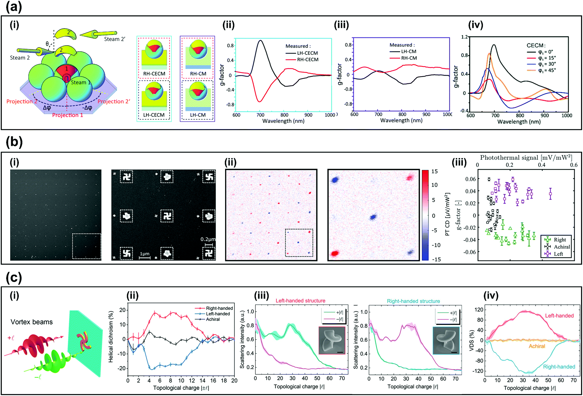 | ||
| Fig. 3 Methods for sensitive chiral sensing. (a) CECM chiral signal.20 (i) Schematic diagram of two-step ADMD on a self-assembled microsphere monolayer and schematic of RH-CECMs, RH-CMs, LH-CECMs, LH-CMs. (ii) Measured g factor of LH-CECM and RH-CECM that was fabricated to achieve θ = 75°, Δφ = ±45°. (iii) Measured g factor of LH-CM and RH-CM that was fabricated to achieve θ = 75°, Δφ = ±45°. (iv) Simulated g-factor of LH-CECMs that was fabricated to achieve φ = 0° (black), 15° (red), 30° (blue), and 45° (magenta). (b) Chiral photothermal imaging.18 (i) (left) SEM image of a 9 × 9 gammadion array and (right) SEM image of the area surrounded by dashed square in (i). (ii) Photothermal dichroism image of (i) and (right) detailed photothermal dichroism image of the dashed part of (ii). (iii) g factor vs photothermal signal of 81 nanostructures that has three different handedness. (c) Measured and simulated HD of the nanostructures.6,17 (i) Schematic of measuring HD illuminated by vortex beam. (ii) HD of the right and left achiral Archimedean spiral. (iii) Measured scattering spectra of left and right-handed helix structure illuminated by focused optical vortices. (iv) HD of the left, right and achiral nanostructure. (c) Reproduction with permission from Ref. 20. (c) Reproduction with permission from Ref. 18. (c-i,and ii) Reproduction with permission from Ref. 6. (c-iii,and iv) Reproduction with permission from Ref. 17. | ||
PT CD has been introduced to achieve highly sensitive CD spectroscopy.19,61–63 PT CD can attain high signal-to-noise ratio by combining highly sensitive photothermal microscopy and an enantioselective signal. Therefore, PT CD can detect chiral signals in small samples,18 for example, left, right and achiral gammadions (Fig. 3b-i).18 The PT CD images clearly show the change of the sign in the PT CD signal that follows the chirality of the nanostructure (Fig. 3b-ii). A signal-to-noise ratio (SNR) of approximately ∼45 with 30 ms integration time is shown, compared to the conventional detection method that uses extinction, which reaches a SNR ∼10 with 1−s integration time.18 The high SNR of the PT CD signal permits detection of individual nanoparticles. The experimentally-measured g-factor with 81 individual nanostructures are shown in (Fig. 3b-iii). The g-factor for left and right-handed gammadions was ∼0.04, and the resolution of the dissymmetry factor was ∼0.004, which indicates a strong ability to detect chirality.
HD also has possible applications for sensitive chirality detection. HD is defined as the difference between the scattering of opposite signs of OAM beam, which is calculated as 2(I+l − I−l)/(I+l + I−l)6 where l is the topological charge of the vortex beam. The topological charge l contributes as a new degree of freedom to widen the domain of optical chirality. When the OAM beam is tightly focused, a longitudinal field component is generated and causes optical chirality in the optical axis.64–67 The advantage of HD is that it only requires monochromatic light with a varying OAM topological charge to detect chirality, whereas CD requires a broadband beam.17 An Archimedean spiral and a helical structure showed strongly different scattering intensities depending on the topological charge of tightly focused vortex beams (Fig. 3c-i).6,17 HD reached 0.2 (l = 8) in the Archimedean spiral (Fig. 3c-ii) and 1.2 (l = 30) in the helical nanostructure (Fig. 3c-iii). Maximum HD was reached when the dimension of the structure matched the dimension of the OAM beam (Fig. 3c-iv). Additionally, the height and diameter of the nanostructure can be manipulated to achieve different HD. Note that as l of the beam is increased, the radius of the beam increases, and increases the singularity point that generates a critical point where HD reduces to zero.6,17
In summary, this section reviewed methods for sensitive chiral sensing including CECM, PT CD, and HD. CECM utilizes the cavity to increase the chiroptical signal, PT CD detects chiral signals in individual nanoparticles due to the high SNR. Lastly, HD only requires a monochromatic light with OAM varying state. These advanced chiral sensing methods will benefit for the practical chiroptical sensing system.
Conclusion
In this minireview, we have summarized advanced 3D bottom-up nanofabrication methods, including self-assembly syntheses and wafer-scale processes, which can overcome the limitations of existing conventional methods. We also introduced single scattering measurements which confirm the strengthening of chiral or helical signals. Chiral metamaterials have the potential to demonstrate sensitive chirality-selective sensing and detecting platforms that may contribute significantly to the biomedical and pharmaceutical industries.68,69 To apply the chiral nanostructure to a practical and commercial on-chip sensing system, a dynamic system, such as an opto-fluidic system that considers the mobility of particles, have been actively researched. Recently proposed advanced materials,70–72 tunable materials,73–76 and machine-learning design methods77–80 empower the development of chiral metamaterials. Furthermore, artificial chiral nanostructures can be utilized in various photonic applications such as chiral metamirrors,81 metaholograms,82–86 metalenses,87,88 multi-mode OAM generators,89 beam steering,90 and color prints.91 These applications can be further improved by analysis of current metasurface and metamaterials that use various optical responses such as Mie-resonance,92–96 geometric phases,97,98 nanogap plasmonics,99,100 nonlinear optics,101 Bragg-reflection,102,103 and spin Hall effect.104–108 Future research could also focus on how tuneable chirality and controllable chiroptical properties can be produced so that the chiral structure is not fixed and the degrees of freedom can be increased.109,110Author contributions
Y.K., H.K., and Y.Y. contributed equally. J.R. conceived the idea and initiated the project of artificial chirality. Y.K., H.K., and Y.Y. mainly wrote the manuscript and reproduced the figures while T.B. and N.J. were partially involved. All authors confirm the final manuscript. J.R. guided all aspects of the work.Conflicts of interest
There are no conflicts to declare.Acknowledgements
This work was financially supported by the POSCO-POSTECH-RIST Convergence Research Center program funded by POSCO, and the National Research Foundation (NRF) grants (NRF-2019R1A2C3003129, CAMM-2019M3A6B3030637, NRF-2019R1A5A8080290, NRF-2018M3D1A1058997). Y.K. and Y.Y. acknowledge the Hyundai Motor Chung Mong-Koo fellowships. Y.K. acknowledges the POSTECHIAN fellowship from POSTECH. Y.Y. acknowledges the NRF fellowship (NRF-2021R1A6A3A13038935) funded by the Ministry of Education, Republic of Korea. H.K. acknowledges the POSTECH Alchemist fellowship.References
- J. Mun, M. Kim, Y. Yang, T. Badloe, J. Ni, Y. Chen, C.-W. Qiu and J. Rho, Light: Sci. Appl., 2020, 9, 139 CrossRef CAS PubMed.
- S. Yoo and Q.-H. Park, Nanophotonics, 2019, 8, 249–261 Search PubMed.
- S. S. Oh and O. Hess, Nano Converg., 2015, 2, 24 CrossRef PubMed.
- J. Kaschke and M. Wegener, Nanophotonics, 2016, 5, 510–523 Search PubMed.
- Y. Yang, Y. Kim, J. Gwak, S. So, J. Mun, M. Kim, H. Jeong, I. Kim, T. Badloe and J. Rho, Realization of Artificial Chirality in Micro-/Nano-scale Three-Dimensional Plasmonic Structures, Chirality Magn. Magn Sep. Phenom. Jt. Eff. Metamater. Struct., 2021, 138, 241–263 CAS.
- J. Ni, S. Liu, G. Hu, Y. Hu, Z. Lao, J. Li, Q. Zhang, D. Wu, S. Dong, J. Chu and C.-W. Qiu, ACS Nano, 2021, 15, 2893–2900 CrossRef CAS PubMed.
- R. M. Kerber, J. M. Fitzgerald, S. S. Oh, D. E. Reiter and O. Hess, Commun. Phys., 2018, 1, 1–7 CrossRef.
- X. Zambrana-Puyalto, X. Vidal and G. Molina-Terriza, Nat. Commun., 2014, 5, 4922 CrossRef CAS PubMed.
- W. Zhang, T. Wu, R. Wang and X. Zhang, Nanoscale, 2017, 9, 5701–5707 RSC.
- T. Wu, W. Zhang, H. Zhang, S. Hou, G. Chen, R. Liu, C. Lu, J. Li, R. Wang, P. Duan, J. Li, B. Wang, L. Shi, J. Zi and X. Zhang, Phys. Rev. Lett., 2020, 124, 083901 CrossRef CAS PubMed.
- E. Hendry, T. Carpy, J. Johnston, M. Popland, R. V. Mikhaylovskiy, A. J. Lapthorn, S. M. Kelly, L. D. Barron, N. Gadegaard and M. Kadodwala, Nat. Nanotechnol., 2010, 5, 783–787 CrossRef CAS PubMed.
- J. K. Gansel, M. Thiel, M. S. Rill, M. Decker, K. Bade, V. Saile, G. von Freymann, S. Linden and M. Wegener, Science, 2009, 325, 1513–1515 CrossRef CAS PubMed.
- J. K. Gansel, M. Latzel, A. Frölich, J. Kaschke, M. Thiel and M. Wegener, Appl. Phys. Lett., 2012, 100, 101109 CrossRef.
- J. Kaschke and M. Wegener, Opt. Lett., 2015, 40, 3986–3989 CrossRef CAS PubMed.
- J. Kaschke, L. Blume, L. Wu, M. Thiel, K. Bade, Z. Yang and M. Wegener, Adv. Opt. Mater., 2015, 3, 1411–1417 CrossRef CAS.
- M. Esposito, V. Tasco, F. Todisco, A. Benedetti, D. Sanvitto and A. Passaseo, Adv. Opt. Mater., 2014, 2, 154–161 CrossRef.
- J. Ni, S. Liu, D. Wu, Z. Lao, Z. Wang, K. Huang, S. Ji, J. Li, Z. Huang, Q. Xiong, Y. Hu, J. Chu and C.-W. Qiu, Proc. Natl. Acad. Sci. U. S. A., 2021, 118, e2020055118 CrossRef CAS PubMed.
- P. Spaeth, S. Adhikari, L. Le, T. Jollans, S. Pud, W. Albrecht, T. Bauer, M. Caldarola, L. Kuipers and M. Orrit, Nano Lett., 2019, 19, 8934–8940 CrossRef CAS PubMed.
- X.-T. Kong, L. K. Khorashad, Z. Wang and A. O. Govorov, Nano Lett., 2018, 18, 2001–2008 CrossRef CAS PubMed.
- C. Tang, F. Chen, J. Du and Y. Hou, Nanoscale, 2020, 12, 9162–9170 RSC.
- S. Xiao, T. Wang, T. Liu, C. Zhou, X. Jiang and J. Zhang, J. Phys. D: Appl. Phys., 2020, 53, 503002 CrossRef CAS.
- M. Hentschel, M. Schäferling, X. Duan, H. Giessen and N. Liu, Sci. Adv., 3, e1602735.
- J. Karst, N. H. Cho, H. Kim, H.-E. Lee, K. T. Nam, H. Giessen and M. Hentschel, ACS Nano, 2019, 13, 8659–8668 CrossRef CAS PubMed.
- M. Wang, J. Dong, C. Zhou, H. Xie, W. Ni, S. Wang, H. Jin and Q. Wang, ACS Nano, 2019, 13, 13702–13708 CrossRef CAS PubMed.
- Y. Y. Lee, N. H. Cho, S. W. Im, H.-E. Lee, H.-Y. Ahn and K. T. Nam, ChemNanoMat, 2020, 6, 362–367 CrossRef CAS.
- N. H. Cho, G. H. Byun, Y.-C. Lim, S. W. Im, H. Kim, H.-E. Lee, H.-Y. Ahn and K. T. Nam, ACS Nano, 2020, 14, 3595–3602 CrossRef CAS PubMed.
- L. Ohnoutek, N. H. Cho, A. W. A. Murphy, H. Kim, D. M. Răsădean, G. D. Pantoş, K. T. Nam and V. K. Valev, Nano Lett., 2020, 20, 5792–5798 CrossRef CAS PubMed.
- H. Kim, S. W. Im, N. H. Cho, D. H. Seo, R. M. Kim, Y.-C. Lim, H.-E. Lee, H.-Y. Ahn and K. T. Nam, Angew. Chem., Int. Ed., 2020, 59, 12976–12983 CrossRef CAS PubMed.
- H. Kim, S. W. Im, R. M. Kim, N. H. Cho, H.-E. Lee, H.-Y. Ahn and K. T. Nam, Mater. Adv., 2020, 1, 512–524 RSC.
- H.-E. Lee, H.-Y. Ahn, J. Mun, Y. Y. Lee, M. Kim, N. H. Cho, K. Chang, W. S. Kim, J. Rho and K. T. Nam, Nature, 2018, 556, 360–365 CrossRef CAS PubMed.
- H.-E. Lee, R. M. Kim, H.-Y. Ahn, Y. Y. Lee, G. H. Byun, S. W. Im, J. Mun, J. Rho and K. T. Nam, Nat. Commun., 2020, 11, 263 CrossRef CAS PubMed.
- L. Dai, P. Liu, X. Hu, X. Zhao, G. Shao and Y. Tian, Analyst, 2021, 146, 1807–1819 RSC.
- Y. Huang, M.-K. Nguyen, A. K. Natarajan, V. H. Nguyen and A. Kuzyk, ACS Appl. Mater. Interfaces, 2018, 10, 44221–44225 CrossRef CAS PubMed.
- J. Ryssy, A. K. Natarajan, J. Wang, A. J. Lehtonen, M.-K. Nguyen, R. Klajn and A. Kuzyk, Angew. Chem., Int. Ed., 2021, 60, 5859–5863 CrossRef CAS PubMed.
- L. Kumar, S. Singh, A. Horechyy, A. Fery and B. Nandan, Membranes, 2021, 11, 318 CrossRef CAS PubMed.
- R. P. Thedford, P. A. Beaucage, E. M. Susca, C. A. Chao, K. C. Nowack, R. B. V. Dover, S. M. Gruner and U. Wiesner, Adv. Funct. Mater., 2021, 31, 2100469 CrossRef CAS.
- K.-C. Yang, C.-T. Yao, L.-Y. Huang, J.-C. Tsai, W.-S. Hung, H.-Y. Hsueh and R.-M. Ho, NPG Asia Mater., 2019, 11, 1–11 CrossRef.
- K.-C. Yang and R.-M. Ho, ACS Macro Lett., 2020, 9, 1130–1134 CrossRef CAS.
- Y. Zhu, L. Han, H. Fan, M. Wang, R. Qi, Y. Zhao and F. He, Macromolecules, 2020, 53, 3217–3223 CrossRef CAS.
- J. Yuan, X. Lu, Q. Li, Z. Lü and Q. Lu, Angew. Chem., Int. Ed., 2021, 133, 12416–12420 CrossRef.
- P. Xu, L. Gao, C. Cai, J. Lin, L. Wang and X. Tian, Angew. Chem., Int. Ed., 2020, 59, 14281–14285 CrossRef CAS PubMed.
- H. Li, X. Mao, H. Wang, Z. Geng, B. Xiong, L. Zhang, S. Liu, J. Xu and J. Zhu, Macromolecules, 2020, 53, 4214–4223 CrossRef CAS.
- A. Tran, C. E. Boott and M. J. MacLachlan, Adv. Mater., 2020, 32, 1905876 CrossRef CAS PubMed.
- Z. Wang, Y. Yuan, J. Hu, J. Yang, F. Feng, Y. Yu, P. Liu, Y. Men and J. Zhang, Carbohydr. Polym., 2020, 245, 116459 CrossRef CAS PubMed.
- X. Zhang, R. Xiong, S. Kang, Y. Yang and V. V. Tsukruk, ACS Nano, 2020, 14, 14675–14685 CrossRef PubMed.
- G. Zhao, Y. Zhang, S. Zhai, J. Sugiyama, M. Pan, J. Shi and H. Lu, ACS Appl. Mater. Interfaces, 2020, 12, 17833–17844 CrossRef CAS PubMed.
- O. Kose, A. Tran, L. Lewis, W. Y. Hamad and M. J. MacLachlan, Nat. Commun., 2019, 10, 510 CrossRef CAS PubMed.
- S. H. Lee, D. P. Singh, J. H. Sung, M.-H. Jo, K. C. Kwon, S. Y. Kim, H. W. Jang and J. K. Kim, Sci. Rep., 2016, 6, 19580 CrossRef CAS PubMed.
- M. M. Hawkeye and M. J. Brett, J. Vac. Sci. Technol., 2007, 25, 1317–1335 CrossRef CAS.
- Z. Wang, B. Ai, Z. Zhou, Y. Guan, H. Möhwald and G. Zhang, ACS Nano, 2018, 12, 10914–10923 CrossRef CAS PubMed.
- Y. Guan, Z. Wang, B. Ai, C. Chen, W. Zhang, Y. Wang and G. Zhang, ACS Appl. Mater. Interfaces, 2020, 12, 50192–50202 CrossRef CAS PubMed.
- Y. Hou, S. Li, Y. Su, X. Huang, Y. Liu, L. Huang, Y. Yu, F. Gao, Z. Zhang and J. Du, Langmuir, 2013, 29, 867–872 CrossRef CAS PubMed.
- H. Ullah, Y. Qu, T. Wang, Y. Wang, Z. Jing and Z. Zhang, Appl. Surf. Sci., 2019, 467–468, 684–690 CrossRef CAS.
- Y. Hou, H. M. Leung, C. T. Chan, J. Du, H. L.-W. Chan and D. Y. Lei, Adv. Funct. Mater., 2016, 26, 7807–7816 CrossRef CAS.
- A. G. Mark, J. G. Gibbs, T.-C. Lee and P. Fischer, Nat. Mater., 2013, 12, 802–807 CrossRef CAS PubMed.
- Z. Wu and Y. Zheng, Adv. Opt. Mater., 2017, 5, 1700034 CrossRef.
- Z. Wu, Y. Liu, E. H. Hill and Y. Zheng, Nanoscale, 2018, 10, 18096–18112 RSC.
- W. Jung, Y.-H. Jung, P. V. Pikhitsa, J. Feng, Y. Yang, M. Kim, H.-Y. Tsai, T. Tanaka, J. Shin, K.-Y. Kim, H. Choi, J. Rho and M. Choi, Nature, 2021, 592, 54–59 CrossRef CAS PubMed.
- X. Yang, M. Li, Y. Hou, J. Du and F. Gao, Opt. Express, 2019, 27, 6801 CrossRef CAS PubMed.
- B. Yeom, H. Zhang, H. Zhang, J. I. Park, K. Kim, A. O. Govorov and N. A. Kotov, Nano Lett., 2013, 13, 5277–5283 CrossRef CAS PubMed.
- A. R. Miandashti, L. K. Khorashad, M. E. Kordesch, A. O. Govorov and H. H. Richardson, ACS Nano, 2020, 14, 4188–4195 CrossRef PubMed.
- S. Adhikari, P. Spaeth, A. Kar, M. D. Baaske, S. Khatua and M. Orrit, ACS Nano, 2020, 14, 16414–16445 CrossRef CAS PubMed.
- S.-Y. Huang, A. K. Singh and J.-S. Huang, Opt. Express, 2021, 29, 23056 CrossRef PubMed.
- G. F. Quinteiro, F. Schmidt-Kaler and C. T. Schmiegelow, Phys. Rev. Lett., 2017, 119, 253203 CrossRef CAS PubMed.
- P. Woźniak, I. De Leon, K. Höflich, G. Leuchs and P. Banzer, Optica, 2019, 6, 961 CrossRef.
- P. Woźniak, I. De Leon, K. Höflich, C. Haverkamp, S. Christiansen, G. Leuchs and P. Banzer, Opt. Express, 2018, 26, 19275 CrossRef PubMed.
- M. Babiker, D. L. Andrews and V. E. Lembessis, J. Opt., 2019, 21, 013001 CrossRef CAS.
- A. Ahmadivand, M. Semmlinger, L. Dong, B. Gerislioglu, P. Nordlander and N. J. Halas, Nano Lett., 2019, 19, 605–611 CrossRef CAS PubMed.
- L. Bonacina, P.-F. Brevet, M. Finazzi and M. Celebrano, J. Appl. Phys., 2020, 127, 230901 CrossRef CAS.
- Y. Yang, G. Yoon, S. Park, S. D. Namgung, T. Badloe, K. T. Nam and J. Rho, Adv. Mater., 2021, 33, 2005893 CrossRef CAS PubMed.
- G. Yoon, K. Kim, D. Huh, H. Lee and J. Rho, Nat. Commun., 2020, 11, 2268 CrossRef CAS PubMed.
- K. Kim, G. Yoon, S. Baek, J. Rho and H. Lee, ACS Appl. Mater. Interfaces, 2019, 11, 26109–26115 CrossRef CAS PubMed.
- I. Kim, M. A. Ansari, M. Q. Mehmood, W.-S. Kim, J. Jang, M. Zubair, Y.-K. Kim and J. Rho, Adv. Mater., 2020, 32, 2004664 CrossRef CAS PubMed.
- I. Kim, W.-S. Kim, K. Kim, M. A. Ansari, M. Q. Mehmood, T. Badloe, Y. Kim, J. Gwak, H. Lee, Y.-K. Kim and J. Rho, Sci. Adv., 2021, 7, eabe9943 CrossRef CAS PubMed.
- I. Kim, J. Yun, T. Badloe, H. Park, T. Seo, Y. Yang, J. Kim, Y. Chung, Y. Chung, J. Rho, J. Rho and J. Rho, Photonics Res., 2020, 8, 1409–1415 CrossRef.
- J. Jang, K. Kang, N. Raeis-Hosseini, A. Ismukhanova, H. Jeong, C. Jung, B. Kim, J.-Y. Lee, I. Park and J. Rho, Adv. Opt. Mater., 2020, 8, 1901932 CrossRef CAS.
- S. So, T. Badloe, J. Noh, J. Bravo-Abad and J. Rho, Nanophotonics, 2020, 9, 1041–1057 Search PubMed.
- S. So, Y. Yang, T. Lee, J. Rho, J. Rho and J. Rho, Photonics Res., 2021, 9, B153–B158 CrossRef.
- J. Noh, Y.-H. Nam, S. So, C. Lee, S.-G. Lee, Y. Kim, T.-H. Kim, J.-H. Lee and J. Rho, Opt. Mater. Express, 2021, 11, 2310–2317 CrossRef CAS.
- T. Badloe, I. Kim and J. Rho, Phys. Chem. Chem. Phys., 2020, 22, 2337–2342 RSC.
- M. Rajaei, J. Zeng, M. Albooyeh, M. Kamandi, M. Hanifeh, F. Capolino and H. K. Wickramasinghe, ACS Photonics, 2019, 6, 924–931 CrossRef CAS.
- H. S. Khaliq, I. Kim, J. Kim, D. K. Oh, M. Zubair, K. Riaz, M. Q. Mehmood and J. Rho, Adv. Opt. Mater., 2021, 9, 2002002 CrossRef CAS.
- M. A. Naveed, M. A. Ansari, I. Kim, T. Badloe, J. Kim, D. K. Oh, K. Riaz, T. Tauqeer, U. Younis, M. Saleem, M. S. Anwar, M. Zubair, M. Q. Mehmood and J. Rho, Microsyst. Nanoeng., 2021, 7, 5 CrossRef CAS PubMed.
- J. Kim, Y. Yang, T. Badloe, I. Kim, G. Yoon and J. Rho, InfoMat, 2021, 3, 739–754 CrossRef.
- G. Yoon, J. Kim, J. Mun, D. Lee, K. T. Nam and J. Rho, Commun. Phys., 2019, 2, 129 CrossRef.
- H. Ren, X. Fang, J. Jang, J. Bürger, J. Rho and S. A. Maier, Nat. Nanotechnol., 2020, 15, 948–955 CrossRef CAS PubMed.
- C. Wang and C. Wang, Optica, 2021, 8, 502–510 CrossRef.
- C. He, T. Sun, J. Guo, M. Cao, J. Xia, J. Hu, Y. Yan and C. Wang, Adv. Opt. Mater., 2019, 7, 1901129 CrossRef CAS.
- Y. Yuan, K. Zhang, B. Ratni, Q. Song, X. Ding, Q. Wu, S. N. Burokur and P. Genevet, Nat. Commun., 2020, 11, 4186 CrossRef PubMed.
- I. Kim, R. J. Martins, J. Jang, T. Badloe, S. Khadir, H.-Y. Jung, H. Kim, J. Kim, P. Genevet and J. Rho, Nat. Nanotechnol., 2021, 16, 508–524 CrossRef CAS PubMed.
- H. L. Liu, B. Zhang, T. Gao, X. Wu, F. Cui and W. Xu, Nanoscale, 2019, 11, 5506–5511 RSC.
- J. Jang, T. Badloe, Y. Yang, T. Lee, J. Mun and J. Rho, ACS Nano, 2020, 14, 15317–15326 CrossRef PubMed.
- J. Jang, T. Badloe, Y. C. Sim, Y. Yang, J. Mun, T. Lee, Y.-H. Cho and J. Rho, Nanoscale, 2020, 12, 21392–21400 RSC.
- C. Jung, Y. Yang, J. Jang, T. Badloe, T. Lee, J. Mun, S.-W. Moon and J. Rho, Nanophotonics, 2021, 10, 919–926 CrossRef CAS.
- T. Lee, J. Kim, I. Koirala, Y. Yang, T. Badloe, J. Jang and J. Rho, ACS Appl. Mater. Interfaces, 2021, 13, 26299–26307 CrossRef CAS PubMed.
- T. Lee, J. Jang, H. Jeong and J. Rho, Nano Converg., 2018, 5, 1 CrossRef CAS PubMed.
- D. Lee, Y. Yang, G. Yoon, M. Kim and J. Rho, Appl. Phys. Lett., 2019, 115, 101102 CrossRef.
- S.-W. Moon, Y. Kim, G. Yoon and J. Rho, iScience, 2020, 23, 101877 CrossRef CAS PubMed.
- I. Kim, J. Mun, W. Hwang, Y. Yang and J. Rho, Microsyst. Nanoeng., 2020, 6, 65 CrossRef CAS PubMed.
- H. Lee, I. Kim, C. Park, M. Kang, J. Choi, K.-Y. Jeong, J. Mun, Y. Kim, J. Park, M. B. Raschke, H.-G. Park, M. S. Jeong, J. Rho and K.-D. Park, Adv. Funct. Mater., 2021, 31, 2102893 CrossRef CAS.
- T. Stolt, J. Kim, S. Héron, A. Vesala, Y. Yang, J. Mun, M. Kim, Mikko. J. Huttunen, R. Czaplicki, M. Kauranen, J. Rho and P. Genevet, Phys. Rev. Lett., 2021, 126, 033901 CrossRef CAS PubMed.
- M. Kim, D. Lee, S. Son, Y. Yang, H. Lee and J. Rho, Adv. Opt. Mater., 2021, 9, 2002226 CrossRef CAS.
- M. Kim, D. Lee, Y. Yang and J. Rho, Opto-Electron. Adv., 2021, 4, 200006 CAS.
- Y. Yang, T. Lee, M. Kim, C. Jung, T. Badloe, D. Lee, S. Lee, H.-J. Lee and J. Rho, IEEE J. Sel. Top. Quantum Electron., 2021, 27, 7300608 CAS.
- M. Kim, D. Lee, T. H. Kim, Y. Yang, H. J. Park and J. Rho, ACS Photonics, 2019, 6, 2530–2536 CrossRef CAS.
- M. Kim, D. Lee and J. Rho, Laser Photonics Rev., 2021, 15, 2100138 CrossRef CAS.
- M. Kim, D. Lee, H. Cho, B. Min and J. Rho, Laser Photonics Rev., 2021, 15, 2000393 CrossRef CAS.
- M. Kim, D. Lee, B. Ko and J. Rho, APL Photonics, 2020, 5, 066106 CrossRef CAS.
- E. S. A. Goerlitzer, R. Mohammadi, S. Nechayev, P. Banzer and N. Vogel, Adv. Opt. Mater., 2019, 7, 1801770 CrossRef.
- Z. Wang, Y. Wang, G. Adamo, J. Teng and H. Sun, Laser Photonics Rev., 2019, 13, 1800276 CrossRef.
Footnote |
| † These authors contributed equally. |
| This journal is © The Royal Society of Chemistry 2022 |