
 Open Access Article
 This Open Access Article is licensed under a
 Creative Commons Attribution 3.0 Unported Licence
Ion-driven nanograin formation in early-stage degradation of tri-cation perovskite films†
Filipe
Richheimer‡
 ab,
David
Toth‡
cd,
Bekele
Hailegnaw
ef,
Mark A.
Baker
b,
Robert A.
Dorey
b,
Ferry
Kienberger
c,
Fernando A.
Castro
a,
Martin
Kaltenbrunner
f,
Markus C.
Scharber
e,
Georg
Gramse
cd and
Sebastian
Wood
*a
ab,
David
Toth‡
cd,
Bekele
Hailegnaw
ef,
Mark A.
Baker
b,
Robert A.
Dorey
b,
Ferry
Kienberger
c,
Fernando A.
Castro
a,
Martin
Kaltenbrunner
f,
Markus C.
Scharber
e,
Georg
Gramse
cd and
Sebastian
Wood
*a
aNational Physical Laboratory, Teddington, Middlesex TW11 0LW, UK. E-mail: sebastian.wood@npl.co.uk
bCentre for Engineering Materials, University of Surrey, Guildford, GU2 7XH, UK
cKeysight Technologies GmbH, Linz, 4020, Austria
dApplied Experimental Biophysics, Johannes Kepler University, Linz, 4020, Austria
eDivision of Soft Matter Physics and LIT Soft Materials Lab, Johannes Kepler University, Linz, 4040, Austria
fDepartment Soft Matter Physics (SoMaP), Johannes Kepler University Linz, 4040, Austria
First published on 7th February 2022
Abstract
The operational stability of organic–inorganic halide perovskite based solar cells is a challenge for widespread commercial adoption. The mobility of ionic species is a key contributor to perovskite instability since ion migration can lead to unfavourable changes in the crystal lattice and ultimately destabilisation of the perovskite phase. Here we study the nanoscale early-stage degradation of mixed-halide mixed-cation perovskite films under operation-like conditions using electrical scanning probe microscopy to investigate the formation of surface nanograin defects. We identify the nanograins as lead iodide and study their formation in ambient and inert environments with various optical, thermal, and electrical stress conditions in order to elucidate the different underlying degradation mechanisms. We find that the intrinsic instability is related to the polycrystalline morphology, where electrical bias stress leads to the build-up of charge at grain boundaries and lateral space charge gradients that destabilise the local perovskite lattice facilitating escape of the organic cation. This mechanism is accelerated by enhanced ionic mobility under optical excitation. Our findings highlight the importance of inhibiting the formation of local charge imbalance, either through compositions preventing ionic redistribution or local grain boundary passivation, in order to extend operational stability in perovskite photovoltaics.
Introduction
Organic–inorganic halide perovskites, with structural formula ABX3, are attractive candidates for next generation photovoltaic devices with power conversion efficiencies close to that of single crystal Si solar cells1 and tandem device efficiencies exceeding 29%.2 Despite the rapid increase in operational performance, thermal and phase instabilities arising from effects intrinsic to perovskites still hinder the progress towards device optimization.3–6 The problems of ionic migration and halide segregation have been successfully tackled through the synthesis of mixed cation perovskites. Alloying methylammonium (MA+) cations with formamidinium (FA+) and Cs+ ions in the A-site has resulted in improved operational stability, while maintaining high operational performance.7,8 Despite the substantial improvements achieved via A-site substitution in such triple-cation perovskites, steady performance decreases are still observed under operational stress in inert conditions.9A key contributor to the loss of operational stability across a range of timescales is ion migration promoted by the application of external bias and illumination during operation.10 Low migration activation energies and a high density of defects11 result in mobile ions migrating towards oppositely charged electrodes to counteract built-in or externally applied electric fields.12,13 In solar cell devices, ion driven degradation effects under operational conditions can be reversible or irreversible in nature,14–17 with the latter often induced by electrochemical reactions at interfaces,15,17,18 elevated temperatures19,20 or environmental agents.21 Interfacial ion accumulation of MA+ cations has been widely demonstrated in single-cation MAPbI3 compositions.13,22 Recently, cation migration kinetics were shown to be greatly accelerated by increasing substitution of MA+ with FA+ ions.23 In contrast, triple-cation compositions are typically reported to show much lower ion migration activity, which is partially attributed to lower defect concentrations in conjunction with kinetic barriers to ion diffusion.24 Nonetheless, studies still demonstrate large bias-induced organic A-site cation migration on a planar lateral electrode geometry.25
Ionic transport in polycrystalline hybrid conductors is strongly affected by the thin film morphology and is dominant along grain boundaries (GB) demonstrated by the faster ionic diffusion26,27 and lower activation energies for ion migration28 compared to grain centres. Consequently, GBs and crystal defects have been widely shown to act as primary degradation pathways.29–32 Electrical modes of scanning probe microscopy (SPM) such as conductive atomic force microscopy (c-AFM) have contributed greatly to relating local microstructure with changes in functional properties. Studies have reported reduced tip sample currents at GBs that expand over time towards grain centres33 as well as other film degradation phenomena27,34,35 including the formation of surface nanograin (NG) structures. Appearance of NGs has been reported as an early-stage manifestation of film degradation under a variety of stressors such as temperature,36,37 ambient environment,38,39 as well as electron beam irradiation.40–42 While NG formation consistently exhibits a probe bias polarity dependence for different perovskite compositions,27,34 the origin of this effect, as well as the specific contributions of the surface microstructure to local instability, are largely unexplored.
In the present work, we elucidate the relationships between different stressors and the characteristics of resulting NG features. The nanoscale resolved local electrical response of a Cs0.05(FA0.83MA0.17)0.95PbI3−xBrx (CsFAMAPbBrI) polycrystalline film was investigated under conditions relevant to full solar cell operation. Charge redistribution induced by applied electric fields and light exposure is linked to NG formation. The proposed degradation mechanism is a result of inhomogeneous charge accumulation between grain centres and GBs, closely linking formation of NGs with ion migration pathways in the film structure. A synoptic model is proposed to accommodate different stress conditions, associating NG formation with the stress induced local charge environment. The proposed intrinsic instability in CsFAMAPbBrI is driven by heterogeneous charge accumulation and hence can be overcome by inhibiting facile ion migration, which is closely linked to the presence of MA+. Replacing MA+ with more stable cation species and applying different grain and surface passivation techniques could inhibit the ion migration and hence degradation of the perovskite components.
Results and discussion
Nanoscale charge environment under operational conditions
Given the typical dimensions of the CsFAMAPbBrI film microstructure, the emergence of early degradation signs due to the interplay of local charge redistribution effects with the polycrystalline morphology was studied using the high spatial resolution capabilities of electrical SPM. Here, photoconductive AFM (pc-AFM) was used as a tool to simulate conditions experienced by a perovskite solar cell active layer under operation by locally applying electrical bias via the probe in addition to external illumination (wavelength: 532 nm). Scanning Kelvin probe microscopy (SKPM) was applied to probe local charge redistribution effects as a result of simulated operational conditions via pc-AFM. Measurements were performed before poling (using SKPM), during poling (pc-AFM) and after poling (SKPM). Forward biasing was achieved by applying a −0.5 V voltage on the probe (with respect to the conductive ITO substrate) in contact with the CsFAMAPbBrI/ITO structure during photoconductive AFM (pc-AFM) measurements, such that the probe was acting as the negative electrode. More details on the application of different SPM modes for poling purposes can be found in the Experimental methods section. The measurement setup during pc-AFM is illustrated in Fig. 1(a), depicting also the side-coupled collimated beam illuminating the measurement area.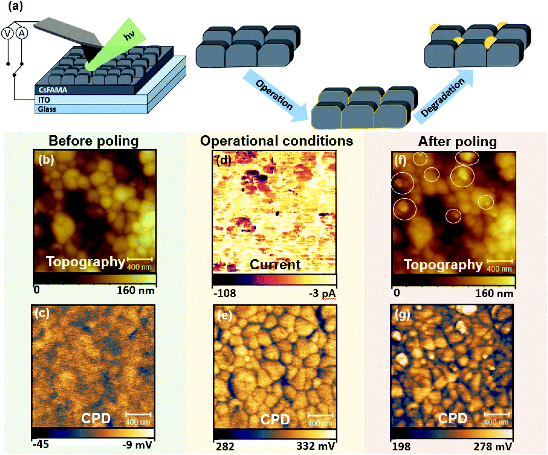 | ||
| Fig. 1 Experimental setup and perovskite sample surface before and after charge injection with metal-coated AFM probe. (a) Schematic of the experimental setup used for photoconductive AFM, where current between the metalised AFM probe and the ITO substrate is recorded. Illustration of morphological evolution across the experiments. (b) AFM topography before poling; (c) SKPM map before poling (dark); (d) pc-AFM measurement at −0.5 V bias and illumination using a 532 nm laser diode at 80 mW cm−2; (e) SKPM under illumination before tip–sample poling; (f) AFM topography after pc-AFM measurement (g) SKPM after poling (dark). Circles in (f) highlight formation of grain-like features after pc-AFM. | ||
The topography and the contact potential difference (CPD) before poling (Fig. 1(b) and (c)) represent the polycrystalline structure of the perovskite, where GBs exhibit lower CPD compared to the grains.27,43 In pc-AFM operation low electrical currents, in the range of tens of pA, were recorded from the grain structures during charge injection as shown in Fig. 1(d). The current collected at the GBs is reduced on average by a factor of 6 (see Fig. S1†), which could be due to locally higher charge extraction barriers. Under illumination, shown in Fig. 1(f), an average surface potential increase of close to 340 mV was obtained with respect to the SKPM map measured in dark conditions. The positive change in the CPD can be attributed to band bending effects at the surface, indicating an intrinsically p-type behaviour and a net negative surface charge under illumination.44 This allows us to construct the energetic landscape across the film thickness (Fig. S2†) when further considering the contact at the back interface with ITO. Interestingly, after the pc-AFM imaging, the subsequent CPD map under dark conditions, shown in Fig. 1(g), records a drop, indicating only a slight decrease of negative surface charge compared to the CPD map obtained during illumination. These changes resulting from the mixed response of electronic and ionic charge carriers are the focus of a number of studies.23,25,43 Further analysis and separation of the effects related to charge carriers of different origin are shown in the discussion following Fig. 3–5.
Importantly, the topography of the scanned region before and after pc-AFM imaging exhibits a significant difference as shown in Fig. 1(b) and (f), respectively. The morphology and location of individual grains within the polycrystalline perovskite film are preserved, indicating that no major structural changes were induced by the measurement. However, we note the appearance of additional granular features on the surface, exhibiting diameters in the range of tens of nanometres. In the following we refer to these features as NGs. Some of the NGs formed during this pc-AFM probing are highlighted by white circles in Fig. 1(f). The NG features formed, shown in Fig. 1(f) exhibit distinctly higher CPDs. Although the CPD difference between adjacent perovskite surfaces and NG features is hard to quantify from these data, the observed contrast of the spatially localised features indicates a difference in chemical composition. These compositional changes must originate from an initiation of chemical degradation within the perovskite film, as mass transfer from the AFM tip gold coating would lead to tip blunting and a subsequent loss in spatial resolution between Fig. 1(b) and (f), which is not observed. In addition, similar structures are induced in absence of a mechanical tip–sample contact in this work.
The results shown in Fig. 1 indicate that when illuminated under forward bias conditions, the formation of the NG structures occurs along with a change of local electronic properties. Such formation of NGs with local compositional differences in the active layer could directly compromise the overall optoelectronic device performance. To understand the chemical composition of the NG structures, a deeper investigation of the formation conditions was required. For this purpose, energy dispersive X-ray spectroscopy (EDX) was conducted on a film surface before and after operational degradation. The resulting spectra are shown in Fig. S3.† Whilst a small decrease in I and Br halides was recorded after poling, a large decrease (40% to 50%, see Fig. S3†) in C and N peaks was measured indicating a loss of MA+ and FA+ organic cations from the system. These results are consistent with recent reports on triple-cation perovskite phase decomposition pathways. Whilst MA-rich perovskite phases are known to decompose into precursor lead-halide salts, FA-rich perovskite converts into a hexagonal δ-phase.45 For triple-cation perovskites, despite being FA-rich, direct decomposition into PbI2 is widely reported,37,46,47 which is explained by the initial phase decomposition dynamics being dominated by the more volatile MA+ cation.46,47 The increased presence of lead-halide products at previously degraded areas is supported by Raman spectroscopy experiments in Fig. S4.†
The impact on the optoelectronic quality of the perovskite due to NG formation was assessed by using photoluminescence (PL) spectroscopy to map areas that were previously exposed to electrical poling. The spatially averaged PL spectra and PL maps are shown in Fig. S5.† The results indicate a drop in PL intensity after AFM probe-based charge extraction. Loss in PL intensity is primarily related to an increase in the non-radiative recombination rate for photogenerated charges. Previous work reported laser-induced perovskite decomposition into PbI2 to have a detrimental effect on PL signal.48 The gradual decrease of PL intensity after contact poling is thus consistent with the EDX results suggesting that NGs are composed of lead–halide compounds.
Separation of stressors promoting surface defect formation
In Fig. 1 NG formation was demonstrated under simultaneous illumination and electrical bias. To distinguish the role of each stressor in NG formation, the perovskite films were separately studied after exposure to dark contact poling (AFM probe-based charge extraction) and illumination conditions. Control samples were exposed to ambient conditions to compare the effect of illumination and bias stressors with ambient atmospheric exposure. The results of exposure to different stressors are depicted in Fig. 2, with a representation of the measurement conditions shown in the top row. Topography scans after exposure under all investigated degradation conditions revealed the formation of NG features. However, stressor-dependent differences are apparent. Under contact poling and illumination conditions depicted in Fig. 2(a) and (b) respectively, NG structures are evenly distributed across individual perovskite grains. Light-induced NG formation depicted in Fig. 2(b) was driven by a focused beam of 633 nm illumination at approximately 3.36 kW cm−2 on a 4 μm2 area irradiated for 60 s The high intensity was used to maximise the number of light-induced NGs. Nonetheless, to further support the relevance of the NG formation under realistic solar cell operation conditions, the growth of NG features is demonstrated after tens of hours at illumination intensities of approximately 1 sun equivalent (80 mW cm−2) at 532 nm, as depicted in Fig. S6.† A common feature of degradation under bias load and illumination conditions is the absence of a preferred formation site of NGs against the film microstructure. Conversely, degradation due to ambient exposure in Fig. 2(c) shows NG formation primarily at the GBs of the polycrystalline film structure. The consistency and reproducibility of selective NG formation at GBs during degradation in ambient environmental conditions is further supported by AFM topography and scanning electron microscopy maps on different films as depicted in Fig. S7.† Similar NG feature distributions have been achieved through simultaneous thermal and humidity induced degradation by placing a CsFAMAPbBrI sample on a hotplate and identified as PbI2via X-ray diffraction experiments.37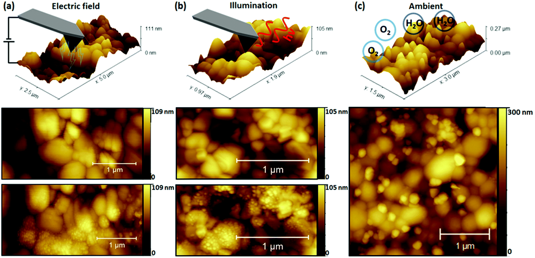 | ||
| Fig. 2 CsFAMAPbBrI degradation under different stress tensors. (a) Localised perovskite stressing in contact poling conditions and topography maps taken before and after. (b) Localised perovskite stressing in open conditions and topography maps taken before and after. (c) Perovskite degradation under ambient conditions and topography maps afterwards. | ||
The possibility that the underlying degradation mechanism in these measurements arises from a pure temperature-driven phase instability due to local heating through electrical resistance or optical absorption was considered through a study of temperature effects in inert conditions. These results are provided in Fig. S8† which compares changes in surface topography resulting from subsequent hot plate heating cycles of the perovskite film. The procedure is further detailed alongside the resulting topography maps in Fig. S8.† The changes of the film morphology indicate a recrystallisation of the mixed perovskite phase, in clear contrast to the appearance of NG-like structures driven by surface decomposition effects.37,47 The absence of NG structures resulting from applying thermal stress under inert conditions suggests that the presence of water and the subsequent deprotonation of the hydrophilic organic cation is required to obtain the recorded local NG formation under thermal stress.46,49 It remains feasible that NG formation under operational conditions is facilitated by local temperature increase during measurements, but it does not appear to be the dominant driver.
A key observation in Fig. 2 is the variation in preferred location of NG formation, suggesting different underlying degradation mechanisms between operational (light, bias load) and ambient stressors. Such contrasting NG nucleation and variability of the NG morphology and dimensions with different stressors was previously observed by comparing electron beam induced surface degradation to ambient degraded MAPbI3 films.42 In the referenced study, different PbI2 polymorphs were identified to form, with the kinetically favored 6H-PbI2 growing on grain surfaces under electron beam radiation, while the thermodynamically favored 2H-PbI2 was promoted by the catalytic deprotonation effect of water molecules at the polar organic cation bond.42 This is highlighted by great similarities between degradation products formed under electrical poling and illumination conditions in the present work and electron beam induced degradation in the work reported before.42 These similarities further hold for degradation morphologies after ambient degradation in both cases. Not only does this support the different underlying degradation mechanisms between operational and ambient stressors, but also the promotion of charge redistribution by the light and current stressors may be critical in the resulting degradation mechanism. Since increasing the density of electronic and ionic charges in organic–inorganic halide perovskites plays a major role in accelerating degradation processes,50 separating the contribution of the charged species can provide further insight into the driving force for NG formation.
Interplay between charge environment and phase stability
Perovskites exhibit hybrid conduction so charge redistribution effects encompass both electronic and ionic charges. In order to separate out the effects of ionic charges, probe-based poling was performed in contact and non-contact modes. The absence of a tip–sample contact in non-contact mode poling prevents the injection of electronic charges provided that the voltages are maintained below the breakdown field of the surrounding medium. Similar approaches have been achieved by the application of insulating contacts for the investigation of ionic migration.51 In the absence of electronic charge carrier injection, charge redistribution is predominantly of ionic nature. First, in Fig. 3 we show results of SKPM imaging after sequential contact electric poling of both polarities. Poling was applied from 0 V to ±2 V and raw datasets containing intermediate voltages are shown in Fig. S9.†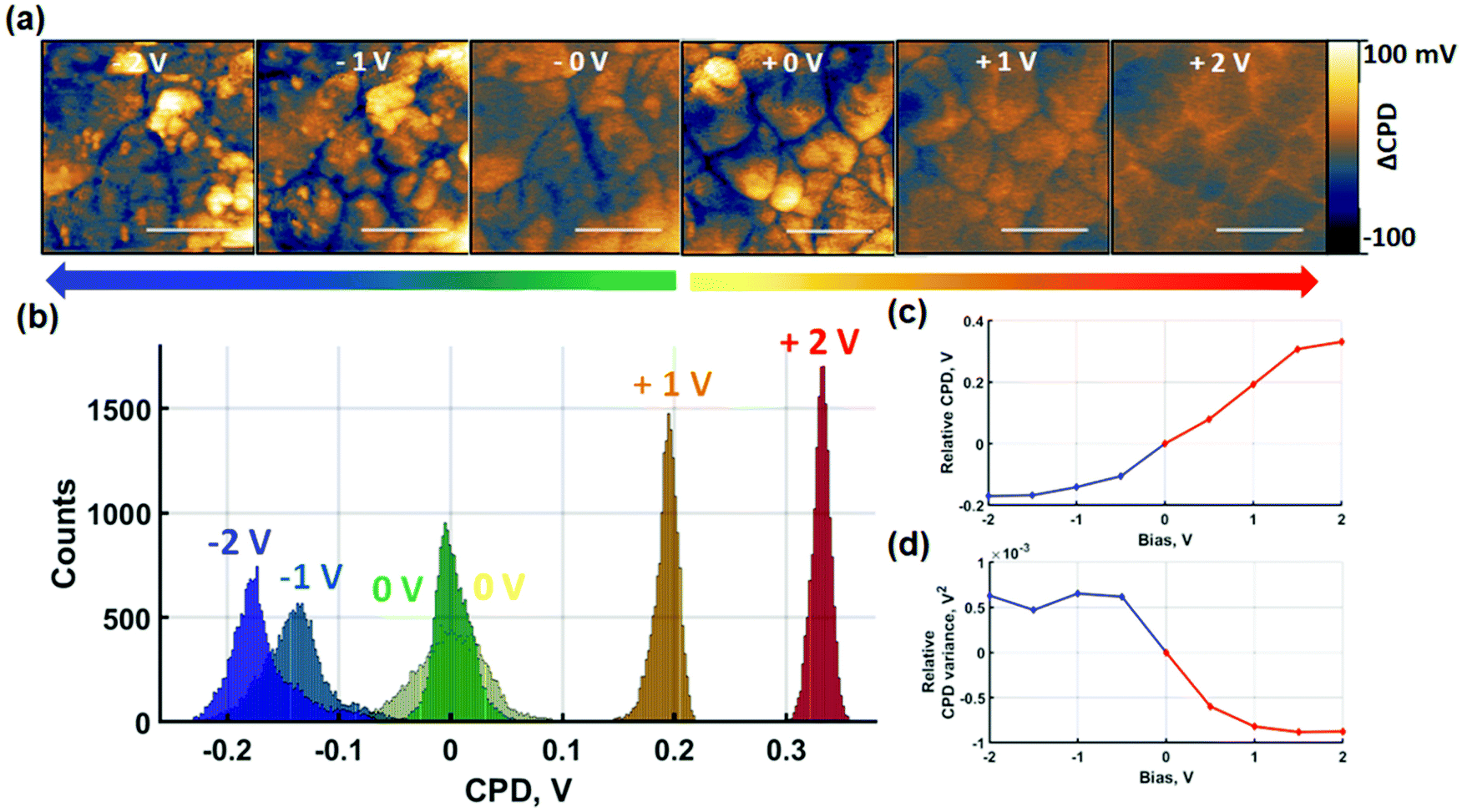 | ||
| Fig. 3 Alternating probe-based contact poling and SKPM measurements. (a) Evolution of spatially resolved SKPM maps centred at 0 V CPD after application of different poling voltages. The mean CPD of each SKPM map was subtracted to facilitate the comparison of the effect of different poling voltages on the relative CPD distribution. (b) Associated relative histogram distributions. Here, all CPD values are subtracted by the mean CPD at 0 V bias of the respective polarity. (c) CPD shift and (d) variance evolution under different poling voltages relative to respective 0 V bias maps. Scale bars represent 400 nm. | ||
After contact poling with the probe at positive bias, two effects can be noted. Firstly, the macroscopic shift of the relative average surface potential in Fig. 3(c) follows a monotonic increase. Secondly, on the nanoscale, this effect is accompanied by a clear loss of CPD contrast between grains and GBs as seen in Fig. 3(a). The former is likely due to a combination of increased densities of trapped electronic charge carriers and slow ionic charge diffusion. The latter is evidenced by the reduced width of the CPD distribution histograms. In the absence of poling, a wide histogram distribution of spatially resolved data is observed, due to the lower surface potential at GBs compared to grain centres. Subsequent poling experiments result in a homogenisation of surface potential reflected by the narrowing of the histograms in Fig. 3(b) and quantified by the variance decrease in Fig. 3(d). Additionally, comparison of the SKPM scans after poling at 1 V and 2 V indicates that the global homogenisation is followed by an inversion of the contrast between grain-boundaries and the grain-interior. While after 1 V bias the CPD at GBs is consistently lower than at the grain interior, the opposite is observed after 2 V bias. As such, the narrowing of the surface potential distribution only shows a snapshot of the relative inversion in CPD contrast between GBs and grain-interior. The intermediate voltages shown in Fig. S9† further resolve the CPD contrast inversion. The surface potential response to poling at negative contact poling voltages shows strikingly different behaviour. The overall film CPD monotonically decreases as a response to increasingly negative voltages. Nanoscale contrast grows with negative bias voltages as seen in Fig. 3(a) and reflected by the broadening of histogram distributions in Fig. 3(b). In addition to the changes in local CPD, Fig. 3(a) also reveals formation of NG features. As a result of the NG formation, although the CPD of the GBs becomes more negative between 0 V and −1 V, the histogram broadening reflects the growth of NG features showing more positive CPD values. The competition between an initial decrease of GB surface potential compared to grain-centres and the increasing CPD contribution of NG features is highlighted in Fig. 3(d). The relative CPD variance follows a consistent increase between 0 V and −1 V resulting from a greater GB to grain-centre contrast. An increase in the variance reflects the build-up of a lateral polarisation of the grain-GB structure. With the appearance of NGs starting from −1 V, the variance shows deviation at subsequent voltages, reflecting NG growth competing with the decreasing GB-grain centre CPD contrast. The spatially averaged CPD equally contains a contribution from the NG formation. While a strong downward trend is observed at lower negative poling voltages for the blue line in Fig. 3(c), the progressive attenuation of the average CPD decrease rate contains larger contributions of the NG CPD. Despite the clear difference observed in CPD behaviour after positive and negative short-circuit poling, the interpretation of the measured effects remains challenging. Nonetheless, the results indicate that NG formation is induced by negative contact poling, while this is not observed at positive voltages of the same magnitude.
To gain insight into the contribution of predominantly ionic species on the CPD response, the same experiments were repeated under non-contact poling conditions as shown in Fig. 4. For consistency, the measurements were performed identically to the contact poling case in Fig. 3. Hence, Fig. 4(a) shows the spatially resolved local CPD evolution and the CPD maps relative to the 0 V poling are depicted as histograms in Fig. 4(b). Poling-induced relative CPD drift and variance are plotted in Fig. 4(c) and (d) respectively.
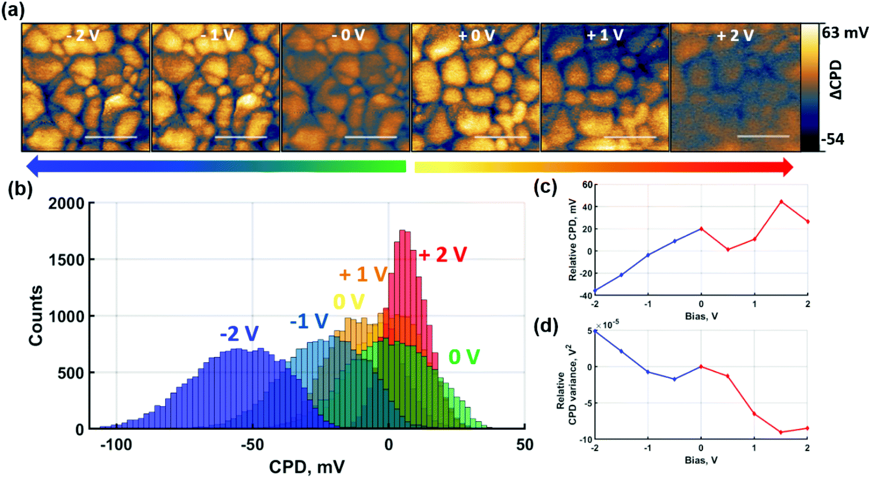 | ||
| Fig. 4 Alternating probe-based non-contact poling and SKPM measurements. (a) Evolution of spatially resolved SKPM maps centred at 0 V CPD after application of different poling voltages and (b) their associated relative histogram distributions. (c) CPD shift and (d) variance evolution under different poling voltages relative to respective 0 V bias maps. A plane flattening was applied to +2 V map in (a) to eliminate background drift due to charge relaxation and better highlight loss in spatial contrast. Scale bars represent 400 nm. | ||
The effect of the non-contact poling at positive voltage depicted in Fig. 4 follows the same trends as the previous contact poling equivalent. An overall homogenisation of CPD is confirmed, which, in the absence of charge injection, can be directly attributed to the accumulation of negatively charged ions at the surface. Although narrowing of the distributions is observed for increasing bias voltage in Fig. 4(d), an inversion of GB CPD contrast is not reached. This can be explained by the overall smaller magnitude of CPD shifts, which is shown in Fig. 4(c) and is observed in the smaller relative narrowing of the histogram distribution in Fig. 4(b). The trend of the CPD at GBs to invert against the grain interior CPD at non-contact poling voltages is demonstrated in Fig. S10,† where the overall poling range was extended up to 5 V. The GB CPD inversion indicates that negatively charged ions, likely in the form of halide ions, accumulate preferentially at GBs rather than grain interiors under the described conditions. At negative non-contact poling voltages, the trends observed at contact poling conditions are similarly confirmed. A consistent decrease of CPD according to Fig. 4(c), albeit smaller in magnitude than after contact poling, confirms the accumulation of positively charged ions at the film surface. The absence of NG formation in this non-contact poling measurement means that the local effects due to poling are revealed with greater clarity. As shown in Fig. 4(b), histogram distributions of spatially resolved data broaden after poling with negative bias, which is more clearly shown by the variance increase in Fig. 4(d). The observed trends shown here are corroborated by measurements where poling was extended to −5 V, shown in Fig. S10(b).† Another significant result from these measurements is the observation of NG formation after non-contact poling with −5 V, which demonstrates that charge redistribution of primarily ionic species can lead to formation of NG structures at high bias.
Results in Fig. 3, 4 and Fig. S10† indicate that formation of NGs can be achieved by both contact and non-contact poling, or in other words with inclusion or exclusion of direct electronic charge injection. Interestingly, nucleation of NGs was only observed under negative bias polling, which additionally resulted in amplification of the initial grain interior-GB CPD contrast. While the observed polarity dependence of NG formation is consistent with findings of previous studies, our results suggest that the NG growth is strongly linked to the laterally induced polarisation between grain interior and GB.43,47,52 If the polarisation drives the NG formation one would expect that positive poling should also cause such film degradation, albeit at higher intensities to compensate the band bending at the bottom interface and/or differences in ionic mobilities. To test this hypothesis, pc-AFM at both polarities applied to the AFM probe was performed. During simultaneous illumination and tip bias in pc-AFM based poling, the combination of both stressors leads to a loss in polarity dependence of NG formation as it is observed for both polarities in the presence of 532 nm illumination with intensity equivalent to 1 sun, as shown in Fig. S11.† Furthermore, NGs are also formed under purely open-circuit poling in the presence of illumination and voltage bias as depicted in Fig. S12.† This reflects a significant increase in ionic mobility under illumination. Strong increases in ionic conductivity by photoactivation have been shown for perovskite structures.53 Increased ion mobility will facilitate charge redistribution and thus accelerate the space charge buildup that drives the NG formation.
Chemical identification via EDX and degradation within a single AFM scan suggests that NG formation is driven by degradation associated with volatility of the bound MA cations promoted by operational stresses. Thus, decomposition into NG structures observed in the present work has origins distinct from previously reported thermal activation. Under operational stimuli, such as bias and illumination, dependence of the lead halide NG formation on electric field distribution can be rationalised as follows; charge redistribution led by electric field build-up between the grain interior and GBs leads to a local reduction of thermodynamic stability of the perovskite phase, facilitating its decomposition through the loss of the volatile organic cations, typically led by bound MA.46,54 It is important to note, that lateral variation of the A-site cation and halide ratios was previously reported for compositions similar to the films of the current study.55,56 While such compositional variation could impact the local stability of the perovskite phase, no direct relation between NG formation sites and CPD distributions prior to the application of operational stressors was found.
For mixed-cation perovskites, as in the present case, the emergence of a vertical ionic space charge may contribute to the aforementioned effect. In this picture, A-site cations migrate to the surface during negative poling and fill negatively charged cation vacancies, which migrate to the bottom (perovskite-ITO) interface. In a mixed cation composition, the methylammonium is the most mobile cation species and thus fills more of vacancies at the film surface compared to its equilibrium distribution in the film bulk. As a result, an A-site cation stoichiometry gradient across the film thickness is formed, with a higher MA+ ion concentration near the negative electrode interface. If the most mobile cation species were equally the most volatile to dissociate under the space charge build up, this would further amplify the resulting imbalance in NG formation for different polarities. An intrinsic cation compositional gradient has been reported before via mass spectroscopy techniques.57 Moreover, redistribution of cations has been observed in triple cation perovskite upon application of external bias,25 with higher concentration of MA+ and FA+ cations accumulating at the negative electrode interface.
Synoptic model of nanograin formation
Having identified and described the nature of the observed NGs, the relation between different stress conditions and NG formation is summarised in Fig. 5. The perovskite film in the equilibrium state under dark conditions and inert atmosphere is represented in Fig. 5(a). Upon deposition of the perovskite film onto ITO a net positive charge at the perovskite bottom interface is formed. In addition, defects, dangling bonds and strain gradients at GBs act as trap sites. GBs exhibit a high defect density and so act as the primary site for moisture penetration;30 and their chemical stability is compromised by their incomplete crystal structure.58 Under exposure to ambient conditions as illustrated in Fig. 5(b), environmental gases promote bond breaking and subsequent escape of organic cations at these sites resulting in the formation of NG structures preferentially at the GBs.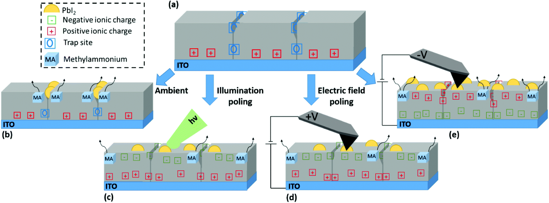 | ||
| Fig. 5 Schematic explanation of charge redistribution and NG formation in the perovskite under different stress tensors. (a) Initially, the GBs of the perovskite accommodate trap sites, while due to band-bending positive ions are present at the bottom interface. (b) Under no external stress, the trap sites at the GBs facilitate a lower activation energy for ion migration and nanograin formation. (c) Under illumination GBs are charged with negative ionic charges. The lateral polarisation of the grain-GB structure lowers the activation energy for nanograin formation. (d) Positive bias applied to the tip results in charging of GBs by negative ionic charges, opposing the initial lateral electric field landscape of the film. (e) Negative bias applied to the tip results in charging of GBs by positive ionic charges, amplifying the initial lateral electric field landscape, resulting in large extent of nanograin formation. | ||
Under illuminated open-circuit poling, as depicted in Fig. 5(c), there is an overall increase in surface potential due to an increasingly negative surface charge. This is partially contributed by photoexcited electrons migrating towards the surface to counteract the built-in field at the free surface as illustrated in Fig. S2,† leading to a CPD increase under illumination. In addition, a slow transient can further increase the CPD over time as shown by SKPM time trace experiments under exposure to light pulses in Fig. S13.† Such a transient due to the ionic contribution was previously discussed in Toth et al.43 Consistent with CPD increases under positive electrical poling experiments with positive biases applied to the tip, it is ionic species of negative charge accumulating at film surface during illumination. The resulting photoinduced spatial imbalance in charge accumulation leads to the formation of a lateral space charge from grain interiors to the surrounding boundaries, which in turn results in lowering the local structural stability thus leading to lead-halide NG growth.
Contact poling is illustrated in Fig. 5(d) and (e) for positive and negative probe bias respectively. Ions of opposite charge accumulate at the film surface, resulting in positive and negative CPD shift respectively. Location-selective charge redistribution on the surface shows different behaviours depending on the polarity. At positive tip bias, a charge polarisation between grain centres and GBs is reached under the application of a sufficiently high voltage magnitude, however, in a direction that opposes the natural polarisation found in an un-poled film. Thus, the reversal from a naturally more positive surface charge at the GBs to a more negative surface charge (with respect to grain centres) opposes the build-up of local space charge. As a result, NG formation is largely suppressed at voltage biases relevant to operational conditions (up to 5 V considered in the present work). At negative bias the pre-existing CPD heterogeneity is monotonically enhanced with greater voltage magnitude. As such, a greater local polarisation is reached, which ultimately promotes the organic cation dissociation. Importantly, the resulting nucleation of NGs happens indiscriminately at GBs and the grain interior.
The correlation between formation of spatially unselective NGs with an increase of a grain interior-GB surface potential for both light and voltage bias stresses supports the hypothesis that a lateral space charge facilitates the dissociation of organic cations. These results demonstrate that a degradation pathway tied to the polycrystalline film morphology arises under operational conditions. Locally, a lack of intrinsic stability is widely associated with the presence of MA minority cations in the A-site,59 which are likely to be responsible for the effects observed in the present work. In full device structures, further interface specific interactions would compete with the reported active layer specific effect, resulting in a drop of the device performance as has been reported under heating and operational conditions.9,38
Conclusions
In the present work, an underlying degradation mechanism of organic–inorganic halide perovskites is investigated by exposing the film to different stress conditions. A combination of scanning probe microscopy methods was employed to study the formation of nanograin structures at the film surface. The observed structures were shown to emerge under light- or voltage-based poling in inert atmosphere. Different degradation stressors were shown to lead to significant differences in the spatial distribution of NGs relative to the local film morphology. Under light and voltage-based poling, NGs form without selectivity towards the polycrystalline film structure. In contrast, degradation under dark conditions in ambient atmosphere showed NG formation predominantly at grain boundaries. EDX analysis on a degraded region identifies the NGs as lead-halide crystals.The loss of locally preferred NG formation sites is related to the local charge environment. Under dark ambient conditions, GBs with lower activation energies due to extended defects and traps act as primary sites for the decomposition of organic cations. In contrast, under the presence of mobile electronic or ionic charges, the local charge distribution on the scale of the perovskite grain structure is changed. A lateral polarisation between grain centres and their boundaries is formed, ultimately leading to nanoscopic NG crystallites that emerge at the surface. The proposed mechanism is further corroborated by the polarity dependence of the lateral polarisation magnitude. Therefore, the NG formation mechanism is rationalised as a reduction of local phase stability driven by the lateral charge gradient. The results presented in this work provide an insight to the local formation mechanisms of degradation products with spatial information down to individual perovskite grains. These findings extend our understanding of the phase instability in triple-cation mixed halide perovskites in terms of the local polycrystalline morphology and operational conditions. This can be used for targeted design of perovskite structures with an aim of reducing photoinduced ionic redistribution. Specifically, obstructing NG formation could be achieved by passivating grain boundary defects to minimise local charge build-up and to delay or reduce the formation of NGs. As such, the sensitivity of the perovskite phase towards its nanoscale local electric environment is emphasised. Further work will be required to assess the direct impact of NG formation in initiating and accelerating operational degradation in full device structures. In addition, methodologies employed in the present work to probe local charge build–up could be of great relevance for assessing the efficacy of passivation methods targeted at inhibiting charge accumulation at GBs and the resulting degradation.
Experimental methods
Perovskite film fabrication
The measurements presented in this study were performed on a Glass/ITO/Perovskite (Cs0.05(FA0.83MA0.17)0.95PbI3−xBrx) structure. Detailed description of sample preparation can be found in ref. 43 and 60. Standard film characterisation techniques such as PL, time-resolved PL and X-ray diffraction of the perovskite compositions equivalent to the ones studies in the present work, as well as photovoltaic performance parameters in a full p–i–n solar cell structure can be found in ref. 60.Scanning probe microscopy
SPM measurements were performed on an AIST-NT Combiscope 1000 AFM system. The microscope was enclosed in a glovebox (Jacomex) and kept under dry nitrogen atmosphere (∼10 ppm O2; 1 ppm H2O). Au-coated 240AC-GG Opus probes from MicroMasch, with nominal resonance frequency at 70 kHz and 2 N m−1 force constant, were used for all experiments. The tip-at-the-front geometry allowed a lateral a 633 nm HeNe laser beam to be coupled in laterally for optical excitation without tip-shadowing and ensured that the scanned area corresponded with the position of the optical excitation spot. The lateral coupling angle was fixed at approximately 30° from the sample plane.(Photo-)Current injection based contact poling experiments were based on contact-mode scanning of a desired area on the perovskite surface. In contact mode the probe is maintained at the repulsive tip sample force regime using the vertical photodetector difference as feedback input. The contact force was set to ensure a continuous electrical contact throughout the scan without inducing any unnecessary damage to the probe Au coating or the perovskite surface. Scanning speed was between approximately 1.5 s and 2.5 s per line with trace and retrace probing, with a scan resolution of 256 lines.
Voltage-based open-circuit poling was performed in a single pass, applying a fixed bias voltage to the tip during non-contact topography scanning. The current preamplifier is kept ‘on’ to ensure that the applied voltages do not lead to an electric breakdown current of the tip–sample dielectric. Considering the typical tip–sample distances during non-contact topography scanning, breakdown currents could be expected for certain applied voltages. Their absence may be explained by the presence of residual airborne contaminants at the film surface which increase the effective dielectric constant in the tip–sample nanogap.
Scanning Kelvin probe microscopy (SKPM) measurements were performed in a two-pass method. On the first pass, the topography was traced in intermittent mode. Subsequently, in a second pass, the previously measured topography trace was followed with the probe lifted by an additional 10 nm from the sample surface. An AC voltage was applied between the tip and sample, with the resulting probe oscillation minimised by adjusting an additional DC component equal to the contact potential difference (CPD). When SKPM is operated with the compensating bias applied to the sample contact, the direction of the CPD change directly reflects the work function shift, therefore the observed contrast indicates shallower work function of the GBs. In the amplitude modulation approach employed here, the applied CPD voltage was adjusted by an additional feedback loop in order to nullify the oscillation amplitude of the probe. Electrical signals were applied to the sample while the probe was connected to the electrical ground. It is important to highlight that when the probe is brought into contact with the sample during contact based poling, contaminants and morphological changes due to wear could impact the surface potential of the probe and thus influence the CPD.61 Although a contribution of this effect cannot be discarded, the consistency of the CPD evolution with the voltage poling polarity, in both contact and non-contact, suggests that work function changes by contaminant pick-up are minimal compared with the effects under study.
Thermally induced morphology change
The involvement of thermal effects in the formation of NGs was probed by alternately measuring the topography of a CsFAMAPbBrI film inside the glovebox and heating the film in a sealed chamber (Linkam HFS600E) under constant N2 flow for durations of approximately 20 minutes (to mimic the duration of an AFM scan). Changes in the film morphology were only observed after heating above 175 °C. The complete recrystallisation of the polycrystalline structure was reached at 200 °C.Photoluminescence
Photoluminescence spectra were recorded by coupling a 532 nm laser diode to the AFM setup. The beam was focused with a 50× magnification and 0.42 NA objective in a top illumination configuration to minimise spot size as opposed to lateral illumination. Low optical exposure at approximately 30 μJ per point was used to prevent photoinduced phase redistribution. The backscattered signal was collected, coupled to a Raman spectrometer (Labram HR Evolution, HORIBA) and dispersed with a 300 lines per mm grating.EDX measurements
A JEOL JSM-6360 LV scanning electron microscope was used to measure the EDX spectra of perovskite films before and after laser exposure at the accelerating voltage of an electron beam of 12 kV. The EDX spectra were scanned on the same area of the sample before and after illumination under a 532 nm laser with intensity equivalent to 10 suns over 60 s.Conflicts of interest
There are no conflicts to declare.Acknowledgements
F. Richheimer and D. Tóth acknowledge the financial support by the European Union's Horizon 2020 Research and Innovation programme under the Marie Skłodowska-Curie grant agreement no. 721874 (SPM2.0). F. Richheimer, F. Castro and S. Wood acknowledge the financial support from the UK Department for Business, Energy and Industrial Strategy (BEIS) through the National Measurement System. D. Tóth and G. Gramse acknowledge the financial support from the European Commission and the state of Upper Austria, EFRE Project IWB 2014-2020, 2018-98292. B. Hailegnaw and M. Scharber acknowledge the financial support of Austrian Research Promotion Agency (FFG) in the framework of the project Flex!PV-2.0-85360. B. Hailegnaw and M. Kaltenbrunner acknowledge the financial support by the ERC Starting Grant “GEL-SYS” under grant agreement no. 757931. The authors would like to thank J. Blakesley and G. Hinds for their constructive comments on the manuscript.References
- Research Cell Record Efficiency Chart, https://www.nrel.gov/pv/assets/pdfs/best-research-cell-efficiencies-rev210726.pdf (accessed August 2021).
- A. Al-Ashouri, E. Köhnen, B. Li, A. Magomedov, H. Hempel, P. Caprioglio, J. A. Márquez, A. B. M. Vilches, E. Kasparavicius, J. A. Smith, N. Phung, D. Menzel, M. Grischek, L. Kegelmann, D. Skroblin, C. Gollwitzer, T. Malinauskas, M. Jošt, G. Matič, B. Rech, R. Schlatmann, M. Topič, L. Korte, A. Abate, B. Stannowski, D. Neher, M. Stolterfoht, T. Unold, V. Getautis and S. Albrecht, Science, 2020, 370, 1300–1309 CrossRef CAS PubMed.
- T. A. Berhe, W. N. Su, C. H. Chen, C. J. Pan, J. H. Cheng, H. M. Chen, M. C. Tsai, L. Y. Chen, A. A. Dubale and B. J. Hwang, Energy Environ. Sci., 2016, 9, 323–356 RSC.
- Y. Rong, Y. Hu, A. Mei, H. Tan, M. I. Saidaminov, S. Il Seok, M. D. McGehee, E. H. Sargent and H. Han, Science, 2018, 361, 6408 CrossRef PubMed.
- J. A. Christians, S. N. Habisreutinger, J. J. Berry and J. M. Luther, ACS Energy Lett., 2018, 3, 2136–2143 CrossRef CAS.
- N. Li, X. Niu, Q. Chen and H. Zhou, Chem. Soc. Rev., 2020, 49, 8235–8286 RSC.
- M. Saliba, T. Matsui, J. Y. Seo, K. Domanski, J. P. Correa-Baena, M. K. Nazeeruddin, S. M. Zakeeruddin, W. Tress, A. Abate, A. Hagfeldt and M. Grätzel, Energy Environ. Sci., 2016, 9, 1989–1997 RSC.
- D. P. McMeekin, G. Sadoughi, W. Rehman, G. E. Eperon, M. Saliba, M. T. Hörantner, A. Haghighirad, N. Sakai, L. Korte, B. Rech, M. B. Johnston, L. M. Herz and H. J. Snaith, Science, 2016, 351, 151–155 CrossRef CAS PubMed.
- K. Domanski, E. A. Alharbi, A. Hagfeldt, M. Grätzel and W. Tress, Nat. Energy, 2018, 3, 61–67 CrossRef CAS.
- M. V. Khenkin, K. M. Anoop, E. A. Katz and I. Visoly-Fisher, Energy Environ. Sci., 2019, 12, 550–558 RSC.
- J.-W. Lee, S.-G. Kim, J.-M. Yang, Y. Yang and N.-G. Park, APL Mater., 2019, 7, 041111 CrossRef.
- C. Eames, J. M. Frost, P. R. F. Barnes, B. C. O'Regan, A. Walsh and M. S. Islam, Nat. Commun., 2015, 6, 7497 CrossRef CAS PubMed.
- Y. Yuan, J. Chae, Y. Shao, Q. Wang, Z. Xiao, A. Centrone and J. Huang, Adv. Energy Mater., 2015, 5, 1500615 CrossRef.
- K. Domanski, B. Roose, T. Matsui, M. Saliba, S. H. Turren-Cruz, J. P. Correa-Baena, C. R. Carmona, G. Richardson, J. M. Foster, F. De Angelis, J. M. Ball, A. Petrozza, N. Mine, M. K. Nazeeruddin, W. Tress, M. Grätzel, U. Steiner, A. Hagfeldt and A. Abate, Energy Environ. Sci., 2017, 10, 604–613 RSC.
- J. Li, Q. Dong, N. Li and L. Wang, Adv. Energy Mater., 2017, 7, 1602922 CrossRef.
- M. Bag, L. A. Renna, R. Y. Adhikari, S. Karak, F. Liu, P. M. Lahti, T. P. Russell, M. T. Tuominen and D. Venkataraman, J. Am. Chem. Soc., 2015, 137, 13130–13137 CrossRef CAS PubMed.
- J. Lim, M. Kim, H. H. Park, H. Jung, S. Lim, X. Hao, E. Choi, S. Park, M. Lee, Z. Liu, M. A. Green, J. Seo, J. Park and J. S. Yun, Sol. Energy Mater. Sol. Cells, 2021, 219, 110776 CrossRef CAS.
- S. Cacovich, L. Ciná, F. Matteocci, G. Divitini, P. A. Midgley, A. Di Carlo and C. Ducati, Nanoscale, 2017, 9, 4700–4706 RSC.
- G. Divitini, S. Cacovich, F. Matteocci, L. Cinà, A. Di Carlo and C. Ducati, Nat. Energy, 2016, 1, 15012 CrossRef CAS.
- A. Kumar, U. Bansode, S. Ogale and A. Rahman, Nanotechnology, 2020, 31, 365403 CrossRef CAS PubMed.
- T. Leijtens, E. T. Hoke, G. Grancini, D. J. Slotcavage, G. E. Eperon, J. M. Ball, M. De Bastiani, A. R. Bowring, N. Martino, K. Wojciechowski, M. D. McGehee, H. J. Snaith and A. Petrozza, Adv. Energy Mater., 2015, 5, 1500962 CrossRef.
- Y. Lin, B. Chen, Y. Fang, J. Zhao, C. Bao, Z. Yu, Y. Deng, P. N. Rudd, Y. Yan, Y. Yuan and J. Huang, Nat. Commun., 2018, 9, 4981 CrossRef PubMed.
- L. Collins, E. S. Muckley, H. Tsai, D. Ghosh, A. J. Neukirch, S. Tretiak, S. V. Kalinin, W. Nie and I. N. Ivanov, ACS Appl. Mater. Interfaces, 2020, 12, 15380–15388 CrossRef CAS PubMed.
- A. Walsh and S. D. Stranks, ACS Energy Lett., 2018, 3, 1983–1990 CrossRef CAS.
- I. M. Pavlovetc, M. C. Brennan, S. Draguta, A. Ruth, T. Moot, J. A. Christians, K. Aleshire, S. P. Harvey, S. Toso, S. U. Nanayakkara, J. Messinger, J. M. Luther and M. Kuno, ACS Energy Lett., 2020, 5, 2802–2810 CrossRef CAS.
- Y. Shao, Y. Fang, T. Li, Q. Wang, Q. Dong, Y. Deng, Y. Yuan, H. Wei, M. Wang, A. Gruverman, J. Shield and J. Huang, Energy Environ. Sci., 2016, 9, 1752–1759 RSC.
- J. S. Yun, J. Seidel, J. Kim, A. M. Soufiani, S. Huang, J. Lau, N. J. Jeon, S. Il Seok, M. A. Green and A. Ho-Baillie, Adv. Energy Mater., 2016, 6, 1600330 CrossRef.
- J. Xing, Q. Wang, Q. Dong, Y. Yuan, Y. Fang and J. Huang, Phys. Chem. Chem. Phys., 2016, 18, 30484–30490 RSC.
- J. S. Yun, J. Kim, T. Young, R. J. Patterson, D. Kim, J. Seidel, S. Lim, M. A. Green, S. Huang and A. Ho-Baillie, Adv. Funct. Mater., 2018, 28, 1705363 CrossRef.
- Q. Wang, B. Chen, Y. Liu, Y. Deng, Y. Bai, Q. Dong and J. Huang, Energy Environ. Sci., 2017, 10, 516–522 RSC.
- Z. Chu, M. Yang, P. Schulz, D. Wu, X. Ma, E. Seifert, L. Sun, X. Li, K. Zhu and K. Lai, Nat. Commun., 2017, 8, 2230 CrossRef PubMed.
- H. Qiu and J. M. Mativetsky, Nanoscale, 2021, 13, 746–752 RSC.
- A. Gomez, S. Sanchez, M. Campoy-Quiles and A. Abate, Nano Energy, 2018, 45, 94–100 CrossRef CAS.
- D. Kim, J. S. Yun, P. Sharma, D. S. Lee, J. Kim, A. M. Soufiani, S. Huang, M. A. Green, A. W. Y. Ho-Baillie and J. Seidel, Nat. Commun., 2019, 10, 444 CrossRef CAS PubMed.
- D. Kim, J. H. Yun, M. Lyu, J. Kim, S. Lim, J. S. Yun, L. Wang and J. Seidel, J. Phys. Chem. C, 2019, 123, 14144–14151 CrossRef CAS.
- R. Dong, Y. Fang, J. Chae, J. Dai, Z. Xiao, Q. Dong, Y. Yuan, A. Centrone, X. C. Zeng and J. Huang, Adv. Mater., 2015, 27, 1912–1918 CrossRef CAS PubMed.
- R. Szostak, J. C. Silva, S.-H. Turren-Cruz, M. M. Soares, R. O. Freitas, A. Hagfeldt, H. C. N. Tolentino and A. F. Nogueira, Sci. Adv., 2019, 5, eaaw6619 CrossRef CAS PubMed.
- B. Conings, J. Drijkoningen, N. Gauquelin, A. Babayigit, J. D'Haen, L. D'Olieslaeger, A. Ethirajan, J. Verbeeck, J. Manca, E. Mosconi, F. De Angelis and H. G. Boyen, Adv. Energy Mater., 2015, 5, 1500477 CrossRef.
- J. Y. Ma, H. J. Yan, M. H. Li, J. K. Sun, Y. X. Chen, D. Wang and J. S. Hu, Nanoscale, 2020, 12, 7759–7765 RSC.
- H. Yuan, E. Debroye, K. Janssen, H. Naiki, C. Steuwe, G. Lu, M. Moris, E. Orgiu, H. Uji-I, F. De Schryver, P. Samorì, J. Hofkens and M. Roeffaers, J. Phys. Chem. Lett., 2016, 7, 561–566 CrossRef CAS PubMed.
- M. U. Rothmann, W. Li, Y. Zhu, A. Liu, Z. Ku, U. Bach, J. Etheridge and Y. Cheng, Adv. Mater., 2018, 30, 1800629 CrossRef PubMed.
- A. Alberti, C. Bongiorno, E. Smecca, I. Deretzis, A. La Magna and C. Spinella, Nat. Commun., 2019, 10, 2196 CrossRef PubMed.
- D. Toth, B. Hailegnaw, F. Richheimer, F. A. Castro, F. Kienberger, M. C. Scharber, S. Wood and G. Gramse, ACS Appl. Mater. Interfaces, 2020, 12, 48057–48066 CrossRef CAS PubMed.
- S. Sadewasser and T. Glatzel, Kelvin Probe Force Microscopy: From Single Charge Detection to Device Characterization, Springer, 2018 Search PubMed.
- B. Charles, J. Dillon, O. J. Weber, M. S. Islam and M. T. Weller, J. Mater. Chem. A, 2017, 5, 22495–22499 RSC.
- W. Tan, A. R. Bowring, A. C. Meng, M. D. McGehee and P. C. McIntyre, ACS Appl. Mater. Interfaces, 2018, 10, 5485–5491 CrossRef CAS PubMed.
- J. Yang, X. Liu, Y. Zhang, X. Zheng, X. He, H. Wang, F. Yue, S. Braun, J. Chen, J. Xu, Y. Li, Y. Jin, J. Tang, C. Duan, M. Fahlman and Q. Bao, Nano Energy, 2018, 54, 218–226 CrossRef CAS.
- J. Barbé, M. Newman, S. Lilliu, V. Kumar, H. K. H. Lee, C. Charbonneau, C. Rodenburg, D. Lidzey and W. C. Tsoi, J. Mater. Chem. A, 2018, 6, 23010–23018 RSC.
- E. Smecca, Y. Numata, I. Deretzis, G. Pellegrino, S. Boninelli, T. Miyasaka, A. La Magna and A. Alberti, Phys. Chem. Chem. Phys., 2016, 18, 13413–13422 RSC.
- J. Byeon, J. Kim, J. Y. Kim, G. Lee, K. Bang, N. Ahn and M. Choi, ACS Energy Lett., 2020, 5, 2580–2589 CrossRef CAS.
- S. T. Birkhold, J. T. Precht, H. Liu, R. Giridharagopal, G. E. Eperon, L. Schmidt-Mende, X. Li and D. S. Ginger, ACS Energy Lett., 2018, 3, 1279–1286 CrossRef CAS.
- X. Deng, X. Wen, C. F. J. Lau, T. Young, J. Yun, M. A. Green, S. Huang and A. W. Y. Ho-Baillie, J. Mater. Chem. C, 2016, 4, 9060–9068 RSC.
- G. Y. Kim, A. Senocrate, T. Y. Yang, G. Gregori, M. Grätzel and J. Maier, Nat. Mater., 2018, 17, 445–449 CrossRef CAS PubMed.
- N. Li, S. Tao, Y. Chen, X. Niu, C. K. Onwudinanti, C. Hu, Z. Qiu, Z. Xu, G. Zheng, L. Wang, Y. Zhang, L. Li, H. Liu, Y. Lun, J. Hong, X. Wang, Y. Liu, H. Xie, Y. Gao, Y. Bai, S. Yang, G. Brocks, Q. Chen and H. Zhou, Nat. Energy, 2019, 4, 408–415 CrossRef CAS.
- T. A. S. Doherty, A. J. Winchester, S. Macpherson, D. N. Johnstone, V. Pareek, E. M. Tennyson, S. Kosar, F. U. Kosasih, M. Anaya, M. Abdi-Jalebi, Z. Andaji-Garmaroudi, E. L. Wong, J. Madéo, Y. H. Chiang, J. S. Park, Y. K. Jung, C. E. Petoukhoff, G. Divitini, M. K. L. Man, C. Ducati, A. Walsh, P. A. Midgley, K. M. Dani and S. D. Stranks, Nature, 2020, 580, 360–366 CrossRef CAS PubMed.
- R. Chatterjee, I. M. Pavlovetc, K. Aleshire, G. V. Hartland and M. Kuno, ACS Energy Lett., 2018, 3, 469–475 CrossRef CAS.
- S. P. Harvey, Z. Li, J. A. Christians, K. Zhu, J. M. Luther and J. J. Berry, ACS Appl. Mater. Interfaces, 2018, 10, 28541–28552 CrossRef CAS PubMed.
- C. Park, H. Ko, D. H. Sin, K. C. Song and K. Cho, Adv. Funct. Mater., 2017, 27, 1703546 CrossRef.
- B.-w. Park and S. Il Seok, Adv. Mater., 2019, 31, 1805337 CrossRef PubMed.
- B. Hailegnaw, G. Adam, H. Heilbrunner, D. H. Apaydin, C. Ulbricht, N. S. Sariciftci and M. C. Scharber, RSC Adv., 2018, 8, 24836–24846 RSC.
- F. Zhang, F. Ullrich, S. Silver, R. A. Kerner, B. P. Rand and A. Kahn, J. Phys. Chem. Lett., 2019, 10, 890–896 CrossRef CAS PubMed.
Footnotes |
| † Electronic supplementary information (ESI) available. See DOI: 10.1039/d1nr05045a |
| ‡ These authors contributed equally to this work. |
| This journal is © The Royal Society of Chemistry 2022 |