
 Open Access Article
 This Open Access Article is licensed under a Creative Commons Attribution-Non Commercial 3.0 Unported Licence
Nanohybrids as a tool to control the dispersion of organic emitters in solution-processed electroluminescent layers†
Jonathan
Phelipot
a,
Payal
Manzhi
bc,
Nicolas
Ledos
d,
Denis
Tondelier
c,
Bernard
Geffroy
 bc,
Pierre-Antoine
Bouit
d,
Jörg
Ackermann
a,
Muriel
Hissler
*d and
Olivier
Margeat
*a
bc,
Pierre-Antoine
Bouit
d,
Jörg
Ackermann
a,
Muriel
Hissler
*d and
Olivier
Margeat
*a
aAix Marseille Univ, CNRS, CINAM, Marseille, France. E-mail: olivier.margeat@univ-amu.fr
bLaboratoire de Physique des Interfaces et des Couches Minces (LPICM), CNRS, Ecole Polytechnique, IP Paris, Palaiseau Cedex, France
cUniversité Paris-Saclay, CEA, CNRS, NIMBE, LICSEN, 91191, Gif-sur-Yvette, France
dUniv Rennes, CNRS, ISCR – UMR 6226, F-35000 Rennes, France. E-mail: muriel.hissler@univ-rennes1.fr
First published on 4th November 2022
Abstract
Fluorescent organic–inorganic nanohybrids based on π-extended hydroxyoxophosphole emitters grafted onto ZnO nanocrystals, have been introduced as an efficient way to control the spatial arrangement of the organic emitters within a host material. The homogeneous dispersion of the emissive nanohybrids within a host matrix is achieved via co-grafting of an additional surfactant, leading to very smooth films with low roughness. Interestingly, the co-grafting of this surfactant not only improves the thin film morphology but also enhances its photoluminescence quantum yield and allows for the easy solution-processing of this material as an emissive layer in a simplified OLED structure. These devices display strongly improved performances, by more than one order of magnitude, compared to OLEDs using pure nanohybrids. These promising results prove the potential of this technique to graft any type of luminophore in efficient solution-processed light-emitting devices.
Introduction
Research efforts on organic light-emitting diodes (OLEDs) have demonstrated practical applications in nowadays flat panel displays thanks to their advantages of flexibility, fast response, high stability or light weight.1–4 In this context, a great variety of emitters that have been used are either molecular (from fluorescent or thermally-activated delayed fluorescent [TADF] organic luminophores to phosphorescent transition metal complexes),5 macromolecular (fluorescent polymers)6 or hybrid organic/inorganic (QD-LEDs).7 So far, most multilayered OLED products are still fabricated by vacuum deposition technologies that require high running cost.8–12 The need for cost-effective OLED products drives considerable developments to reach innovative materials and fabrication techniques suitable for low-cost and large-area manufacturability of OLEDs. In this respect, solution-process techniques, such as spin coating, blade coating, roll-to-roll or ink-jet printing, show great potential in achieving these goals.13,14 As one of the key materials, highly-efficient solution-processable emitting materials are essential for printed OLEDs. To achieve such property, the emitters (either fluorescent, phosphorescent or TADF) are generally dispersed as guests in suitable concentrations into host materials displaying favorable morphological properties.15 The appropriate guest–host combination selection plays a key role in determining the emissive characteristics in the film state to avoid either morphological inhomogeneities or detrimental emitter–emitter interactions (such as triplet–triplet annihilation). However, solution-processing of host–guest-doped OLEDs faces well-known phase separation problem, inducing serious aggregation of the molecules and resulting in emission quenching.16,17 Although some specific approaches have shown how to avoid this problem,18,19 controlling the dispersion of organic emitters in a host material by solution approach remains a key challenge in the field. Indeed, a tool to control the emitters’ arrangement in the host material would allow for the unrestricted use of all promising types of luminophores.We recently showed that nanohybrids made from the grafting of fluorescent organic emitters onto zinc oxide (ZnO) nanocrystals present aggregation-induced emission (AIE) effects leading to highly photoluminescent thin films.20 However, the OLED devices made from pure nanohybrids displayed limited performances (luminance reaching 60 cd m−2 at 50 mA cm−2) mainly due to a detrimental morphology of the active layer affecting the charge transport. In the present work, we show that dispersion of these nanohybrids within a polymeric host material is a promising approach to greatly enhance the performance of the OLEDs. More importantly, we demonstrate that co-grafting of the organic emitter together with an additional surfactant is an efficient way to control the spatial arrangement of the emitters within a host material (polyvinylcarbazole with oxadiazole). Indeed, the dispersion of the emissive nanohybrids within the host matrix is controlled using classical surfactants for nanocrystals, such as oleic acid. OLEDs devices were then prepared using homogeneously dispersed nanohybrids films with greatly enhanced luminance (reaching 1000 cd m−2 at 50 mA cm−2) compared to the pure nanohybrids film, thus highlighting the potential of this approach.
Design of the emissive nanohybrid layer
Morphology control of the nanohybrid layer
To design the fluorescent nanohybrids (referred as N), we relied on the use of π-extended hydroxyoxophosphole emissive ligands (referred as L). Hence, we and others showed that these compounds allow to generate highly luminescent hybrid materials after grafting on inorganic substrates (SiO2, ZnO, HgS).20–22 Here, according to our reported strategy, L is grafted in solution onto the surface of 6 nm large ZnO nanoparticles (Fig. 1(a) and (b)). As previously shown, the resulting nanohybrids present aggregation-induced emission (AIE) after grafting of the ligand L, explaining the change from low emissive solution to highly emissive solid state.20 In our previous work, the solution-processing of electroluminescent layers based on pure nanohybrids films lead to OLEDs with limited device performance due to morphology inhomogeneities which strongly affected the charge transport as well as the reproducibility of the devices. Indeed, rough layers were obtained, due to undesirable aggregates causing electrical short-circuits and non-homogeneous light emission. To improve both charge transport properties and morphology of the emissive layer, we decided to use classical host/guest structure,23 through the incorporation of the nanohybrids as guest emitters within a host matrix M, leading to a layer referred as M:N as depicted on Fig. 1(c). The association of the polymer polyvinylcarbazole (PVK) with an oxadiazole derivative (OXA) was chosen as host matrix for the nanohybrids. Indeed, it has been reported that PVK, associated to oxadiazole or carbazole derivatives to ensure the electron transport, is an excellent candidate to host wide types of fluorescent or phosphorescent emitters.24,25 The incorporation of nanoparticles with diameter about 5 nm to more than 100 nm within this polymer as host matrix has also been reported.26 Moreover, many studies on the influence of the guest concentration were done, which is a key parameter for the OLED device performances.26,27 | ||
| Fig. 1 Schemes of (a) the individual fluorescent ligand L and nanoparticles ZnO, (b) the nanohybrids N, and (c) the emissive layers using dispersed nanohybrids within the host material with (M:N:OA) or w/o (M:N) the use of oleic acid. | ||
To investigate the morphology of the layer and evaluate the aggregation of the nanohybrids within the host, Transmission Electron Microscopy (TEM) was employed. For sample preparation, a modification of the floating-layer technique was applied.28 First, sacrificial PEDOT:PSS was coated on a substrate before the spin coating of M:N emissive layer on top. After a brief annealing to dry the layers, the PEDOT:PSS film was dissolved in deionized water. Floating thin films of the emissive layer were then recovered and deposited on a holey carbon-coated TEM grid, as shown in Fig. 2(a). The emissive layer presented in the following part is referred as M:N10 sample, using a solution containing 10% w/w of nanohybrids with respect to the host matrix. The resulting TEM images are represented in Fig. 2(b) and (c) at two different magnifications. From the large area in Fig. 2(b), the layer M:N10 reveals nanohybrid aggregates over a micron scale, highlighted on the picture by the white-dotted circles. The presence of high amounts of aggregated nanohybrid structures is confirmed in Fig. 2(c), proving the low ability of the nanohybrids to be homogeneously dispersed within the host matrix. These undesirable aggregates generate electrical short-circuits and therefore need to be removed to obtain functional and reproducible OLED devices. For this purpose, to avoid the agglomerate formation and improve the homogeneous dispersion of the nanohybrids within the host, a low amount of surfactant was used as additive to the M:N10 solution. In this respect, oleic acid (OA), a classical surfactant for the dispersion of nanocrystals in solution, was chosen.29
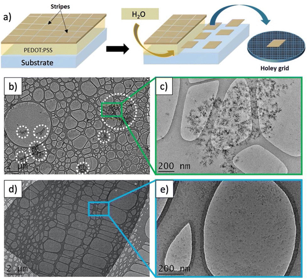 | ||
| Fig. 2 (a) Scheme of the floating-layer technique used for depositing film on the holey carbon coated TEM grid. (b) and (c) TEM images of the layer M:N10 at two magnifications. (d) and (e) TEM images of the layer M:N10:OA at two magnifications. | ||
The layer referred as M:N10:OA corresponds to the blend including the OA treatment in solution (addition of 0.2% v/v). The resulting TEM images are represented in Fig. 2(d) and (e) at two different magnifications. Interestingly, the M:N10:OA layer morphology is totally different from the one obtained with M:N10. Even if slightly more dense areas composed of nanohybrids are noticeable, no aggregate can be found over the whole layer. The OA treatment appears as an efficient method to avoid the formation of aggregates and to ensure the homogeneous dispersion of the nanohybrids. Moreover, the same trends were observed when using other ratios of nanohybrids, as in the case of solutions containing 5 or 15% w/w of nanohybrids with respect to the host matrix, layers referred as M:N5 and M:N15, that present the same morphology improvement using OA, i.e.M:N5:OA and M:N15:OA respectively (Fig. S1, ESI†). We also studied the impact of the concentration of OA to further improve the nanoscale morphology of M:N10:OA layer. It was found that employing lower amounts of OA in solution systematically leads to the formation of aggregates. On the contrary, increasing the amount of OA in the solution (from 0.2 to 0.6% v/v) does not further improve the morphology of the layer (Fig. S2, ESI†). Thus, the value of 0.2% v/v of OA appears as an optimal value to limit any excessive use of this surfactant. The morphology of the nanohybrids within the layer was also studied using Secondary-Electron Microscopy (SEM) on a cross-section of the sample (Fig. S3, ESI†) to determine the vertical dispersity of the nanohybrids. Even if the contrast is very weak, the nanohybrids appear to be present over the whole 50 nm thick layer, with slightly more dense areas at the top of the layer, however ruling out any clear vertical segregation.
The surface morphology was further studied by Atomic Force Microscopy (AFM). AFM images performed on layers containing 10% of nanohybrids, processed with or w/o the use of OA via spin-coating, are presented in Fig. 3, while the related roughness values of the layers are given in Table 1. In the absence of OA, M:N10 layer surface confirms the presence of irregular nanohybrid aggregates within the host matrix, large on a micron scale and as height as 80 nm (Fig. 3(a) and (b)). This inhomogeneous surface is characterized by a very high roughness, measured at 11.1 nm from the 10 × 10 μm image. On the opposite, the M:N10:OA emissive layer presents a very smooth surface morphology, without any noticeable aggregate over the whole surface (Fig. 3(c) and (d)), as already pointed out by the SEM cross-section image. The surface roughness is, as expected, much lower and measured at 1.1 nm from the same 10 × 10 μm scale. The same trends were observed with the other ratios of nanohybrids (Fig. S4, ESI† and Table 1). The M:N5 and M:N15 thin films present high roughness values of 6.0 and 4.8 nm, respectively, caused by the presence of underlaying aggregates. After OA addition in the solution, the roughness of the resulting thin films decreases again significantly to reach 1.4 nm (M:N5:OA) and 1.6 nm (M:N15:OA). These low roughness values are in the range of those obtained in other spin-coated guest–host films used in electroluminescent OLED devices.23,26,30
 | ||
| Fig. 3 AFM images of the layer M:N10 at 10 × 10 μm scale (a) and 5 × 5 μm scale (b). AFM images of the layer M:N10:OA at 10 × 10 μm scale (c) and 5 × 5 μm scale (d). | ||
| M:N5 | M:N5:OA | M:N10 | M:N10:OA | M:N15 | M:N15:OA | |
|---|---|---|---|---|---|---|
| RMS roughness (nm) | 6.0 ± 0.6 | 1.4 ± 0.1 | 11.1 ± 1.0 | 1.1 ± 0.1 | 4.8 ± 0.5 | 1.6 ± 0.1 |
The use of 0.2% v/v of OA as additional surfactant appears as an efficient treatment of the host/guest solution to avoid nanohybrids aggregates and ensure the homogeneous dispersion of the nanohybrids within the matrix, leading to smooth film with low roughness, as required to elaborate reproducible and functional LED devices. The impact of this additive on the optical and electronic properties is addressed in the next paragraph.
The role of OA on the luminescence properties
To determine the effect of OA on the optical properties, the absorption and emission spectra of the nanohybrids with and w/o OA addition were studied when dispersed in the host matrix (samples M:N10 and M:N10:OA, respectively). As a reference, the pure emitter L dispersed in the host matrix is also reported (M:L). The main absorption band of L in diluted solution(λabs = 400 nm, Fig. 4(a)) appears to be slightly blue-shifted after formation of the nanohybrids, as previously observed.20 Indeed, the spectra of M:N10 and M:N10:OA are very similar with λabs = 390 nm. However, the spectra of these two samples differs at higher wavelength (λ > 500 nm) as, in contrast to M:N10:OA, the M:N10 display light scattering signal caused by the presence of nanohybrids aggregates. The absence of light scattering from M:N10:OA unambiguously reveals that the OA treatment allows to homogeneously disperse the nanohybrids within the matrix. The presence of aggregates in absence of OA treatment in M:N10 is also observed on the absorption spectra of the resulting layers (Fig. S5, ESI†). | ||
| Fig. 4 Absorption spectra in chlorobenzene solution (a) and emission spectra (λex = 400 nm) of the resulting films (b) of M:L, M:N10 and M:N10:OA on glass substrate. | ||
Emission spectra were recorded on the thin films with an excitation at λex = 400 nm, i.e. at the maximum absorption of the emitter L and thus avoiding any emission from the matrix or from ZnO nanocrystals (Fig. 4(b)). The pure organic emitter in the matrix, M:L, presents a strong green emission ranging from 440 nm to 650 nm, as expected for the emission of this molecule alone20 and showing the limited influence of the host matrix on the emission wavelength. The nanohybrids containing films M:N10 and M:N10:OA both present the typical L emission.
To quantitatively compare these emission properties, photoluminescence quantum yields (PLQYs) were determined using an integrating sphere according to “John de Mello” method,31 which is independent on the layer thickness. The PLQYs were measured for the matrix layers containing different mass ratios of pure emitter L or nanohybrids N, with or w/o OA treatment (Table 2). The PLQYs for X = 5% and 10% follow the same trend, with PLQYs about 10–12% for M:L, being in the same range at 11–14% for M:N and surprisingly reaching values as high as 31–35% for M:N:OA. The PLQY for X = 15% starts with slightly higher values about 22–24% for M:L15 and M:N15 but also reaches the same high value of 33% for M:N15:OA. The OA treatment clearly shows that homogeneously dispersed nanohybrids in the matrix is the key to enhance the PLQY (by a factor ∼2–3). While the OA ligands improve mainly the solubility of the nanohybrids, we address the PLQY increase in the emissive films to a higher amount of grafted emitters on the ZnO nanoparticle surface, as the overall available ZnO surface is larger due to the absence of aggregates already in solution. To understand the optical and morphological properties of the M:N15:OA layer more in detail, we varied OA quantity by comparing the PLQY of M:N10:OA layers, containing respectively 0.2%, 0.4% and 0.6% v/v of OA (Table S1, ESI†). It was proven in the previous part that the amount of OA in M:N:OA has no significant impact on the surface morphology of the layer. As it can be seen in Table S1 (ESI†), the variation of the OA concentration has also no impact on the PLQY of the luminescent material. We can thus consider that with 0.2% of OA, all fluorescent ligands are already grafted at the ZnO surface, while using additional OA would have a negative impact on the charge injection or transport within the emitter film.
| Sample name | M:Lx | M:Nx | M:Nx:OA | |
|---|---|---|---|---|
| PLQY (%) | x = 5% | 12 ± 1 | 11 ± 1 | 31 ± 3 |
| x = 10% | 10 ± 1 | 14 ± 1 | 35 ± 3 | |
| x = 15% | 24 ± 2 | 22 ± 2 | 33 ± 3 |
In conclusion, the OA treatment not only helps to obtain smooth films of homogeneously dispersed nanohybrids, but also enhances the luminescence of the layers, without modifying the emission wavelength, as usually observed with AIE luminophore. The study is completed in the following part by comparing the performances of OLED devices using M:N:OA based electroluminescent layer.
OLED devices using emissive nanohybrid layer
The different nanohybrids were studied as emitting layer in simple OLED structures. The device structure (Fig. 5(a)) consists of a classical ITO/PEDOT:PSS/M:N:OA/BCP/Alq3/LiF/Al stack with 0.3 cm2 of active surface, the emitting layer M:N:OA being solution-processed by spin-coating (see the ESI† for fabrication details). The current density–voltage–luminance (J–V–L) curves of the diodes were measured to optimize the device performances. Importantly, for all matrix compositions including nanohybrids, the electroluminescence spectrum corresponds to the photoluminescence spectrum of nanohybrids included in matrix, with a maximum emission in the green region at 520 nm (Fig. 5(b)). The inset shows a photograph image of the diode working at 50 mA cm−2 having homogeneous emission over the whole emitting surface. As a reference, we processed diodes using only the PVK/OXA matrix as electroluminescent layer, that show only weak emission in the blue region (maximum emission at 470 nm – Fig. S6, ESI†), characteristic of PVK/OXA. This proves that the green emission in M:N:OA devices originates from the electroluminescence of the nanohybrids. At this point, it has to be pointed out that a reference device using the incorporation of only emitter “L” as guest within the host matrix (i.e. without ZnO introduction) could not be measured. Indeed, such materials lead to very rough films, causing short-circuits in the devices. | ||
| Fig. 5 (a) Scheme of the LED device structure, (b) electroluminescent spectra measured at 50 mA cm−2 (inset: photograph image of the device), (c) J–V curves of the different M:Nx:OA samples and (d) corresponding JVL curves for the best performing M:N10:OA sample. | ||
The device optimization was first realized by varying the thickness of the electroluminescent layer M:N:OA between 40 nm and 100 nm (see Fig. S7 and related performances in Table S2, ESI†). The best performing OLEDs were obtained with emission layer of 50 nm thickness leading to EQE value of 0.71%, luminance efficiency of 1.84 cd A−1 and 0.82 lm W−1 in power efficiency. Drops of the overall performances were observed for the active layers thicker than 50 nm, with EQE of 0.34%. For the lowest thickness, at 40 nm, the threshold voltage slightly increased, but the overall performances remained close to the ones measured for the 50 nm thick device. However, in the case of this 40 nm thick layer, and only for this one, the devices degraded fast under high voltage and the reproducibility was low, which may be attributed directly to the very thin active layer. Further optimizations with other parameters were thus realized using electroluminescent layer thickness at 50 ± 5 nm. The second set of optimizations concerned the determination of the optimal OA amount for nanohybrid preparation. The impact of the concentration of OA in M:N:OA layers on the performance of the OLEDs was studied by elaborating devices with OA amount ranging from 0.05% to 0.6% v/v (see Fig. S8 and related performances in Table S3, ESI†). This study clearly reveals that 0.2% v/v is the optimal OA concentration to obtain the best devices. Indeed, at higher OA concentrations, the overall parameters were quickly degraded, with increase of the threshold voltage from 4 V to 7 V, and drops of the EQE from 0.71% to 0.34%, power efficiency from 0.82 lm W−1 to 0.27 lm W−1 and luminance efficiency from 1.84 cd A−1 to 1.32 cd A−1. These performance losses were attributed to the insulating behavior of the OA fatty acid at these excessive concentrations. At lower OA concentrations, the overall parameters were less affected, with even a slight increase in the luminance efficiency reaching 1.98 cd A−1 at 0.1% v/v of OA. However, for concentrations of OA below 0.2%, a clear degradation of the electroluminescent layer morphology was frequently observed in the devices (due to the formation of aggregates as seen in the part 2.1), clearly lowering the performance reproducibility.
In the previous parts, it was shown that the amount of nanohybrids incorporated within the matrix was not affecting the surface morphology (RMS roughness between 1.1 and 1.6 nm) neither the photoluminescence of the layer (PLQY between 33 and 35%). Such layers were all good candidates to prepare OLED devices. Electroluminescent devices were thus realized using matrices containing different mass ratios of nanohybrids (M:Nx:OA samples) with ratios ranging from X = 0% (pure matrix film) to 20%, under optimized conditions i.e. 50 nm thick active layer and 0.2% v/v of OA (see Fig. 5(c) and related performances in Table 3). By adding more than 10% of nanohybrids in the matrix, the threshold voltage consequently increased from 4 V to more than 9 V, together with lower EQE, power and luminescence efficiencies. This suggests that the presence of a large amount of nanohybrids negatively affects the charge injection and transport properties of the matrix. Using lower ratios of nanohybrids in M:Nx:OA layers, i.e. 5% and 10%, the performance of the OLEDs was improved and comparably high, reaching the same EQE value of 0.71% with power efficiencies of 0.66 and 0.82 lm W−1 and luminance efficiencies of 2.00 and 1.84 cd A−1, respectively. However, a significant lower threshold voltage of 4 V was obtained for M:N10:OA compared to 6 V measured for M:N5:OA. Thus, the best devices were obtained using M:N10:OA as electroluminescent layer. These devices reached a maximum luminance at 1000 cd m−2 at a current density of 50 mA cm−2, as shown in Fig. 5(d). Compared to our previous work, in which an electroluminescent layer made from the pure nanohybrids led to OLEDs with a maximum luminance of only 60 cd m−2, the developed co-grafting technique of emissive ligand and OA ligand, in combination with the use of a host matrix, provides performance enhancement of more than one order of magnitude.
| x% in M:Nx:OA | 0% (ref) | 5% | 10% | 15% | 20% |
|---|---|---|---|---|---|
| Threshold voltage (V) | 4 | 6 | 4 | 8 | 9 |
| EQE (%) | 0.18 | 0.71 | 0.71 | 0.58 | 0.34 |
| Power efficiency (lm W−1) | 0.12 | 0.66 | 0.82 | 0.36 | 0.24 |
| Luminance efficiency (cd A−1) | 0.28 | 2.00 | 1.84 | 1.81 | 1.20 |
Conclusions
Solution-processable materials for organic light-emitting diodes require emitters well-dispersed as guests into the host material. This needs homogeneous dispersion to avoid morphological inhomogeneities, aggregates, phase separation issues or detrimental emitter–emitter interactions. In this work, organic–inorganic nanohybrids were used as an efficient way to control the spatial arrangement of the organic emitters within the host material. The homogeneous dispersion of the emissive nanohybrids within the matrix appears to be assisted by the co-grafting of a surfactant such as oleic acid, leading to very smooth films with low roughness. Interestingly, we proved that the oleic acid treatment enhances the PLQY of the thin films, due to an easier emitter grafting on the better accessible nanocrystal surface in the absence of aggregates. The solution-processing of this material as emissive layer in simple OLED structure led to device with strongly improved performances, by more than one order of magnitude, compared to OLEDs using pure nanohybrids. The successful combination of grafting two ligands, one controlling the emission properties of the hybrid nanostructure and one governing the dispersion within the host matrix, into efficient nanohybrids points towards a highly versatile strategy to adapt a large pallet of organic emitters for efficient solution-processed light-emitting devices. Future work will explore the combination of the presented nanohybrids within more efficient hosts with more suitable ambipolar charge transport or using graftable emitters with improved emission properties (different colors of emission, higher PLQY or presenting TADF properties).Experimental section
Detailed syntheses and characterizations of all compounds, details of equipment and device elaboration are given in ESI.†Conflicts of interest
There are no conflicts to declare.Acknowledgements
This work is supported by the Ministère de la Recherche et de l’Enseignement Supérieur, the CNRS, the Région Bretagne (ARED grant to NL), the French National Research Agency (ANR Fluohyb ANR-17-CE09-0020). The authors thank CINaM staff A.Ranguis for AFM measurements, D.Chaudanson and A.Altié for electron microscopy.References
- K. S. Yook and J. Y. Lee, Adv. Mater., 2014, 26, 4218–4233 CrossRef CAS PubMed.
- D. Ma, T. Tsuboi, Y. Qiu and L. Duan, Adv. Mater., 2017, 29, 1603253 CrossRef PubMed.
- Y. Liu, C. Li, Z. Ren, S. Yan and M. R. Bryce, Nat. Rev. Mater., 2018, 3, 18020 CrossRef CAS.
- M. Y. Wong and E. Zysman-Colman, Adv. Mater., 2017, 29, 1605444 CrossRef PubMed.
- N. Armaroli and H. J. Bolink, Photoluminescent Materials and Electroluminescent Devices, Springer International Publishing, Cham, 2017 Search PubMed.
- H. Peng, X. Sun, W. Weng and X. Fang, Polymer materials for energy and electronic applications., Academic Press, 2016 Search PubMed.
- B. S. Mashford, M. Stevenson, Z. Popovic, C. Hamilton, Z. Zhou, C. Breen, J. Steckel, V. Bulovic, M. Bawendi, S. Coe-Sullivan and P. T. Kazlas, Nat. Photonics, 2013, 7, 407–412 CrossRef CAS.
- T. A. Lin, T. Chatterjee, W. L. Tsai, W. K. Lee, M. J. Wu, M. Jiao, K. C. Pan, C. L. Yi, C. L. Chung, K. T. Wong and C. C. Wu, Adv. Mater., 2016, 28, 6976–6983 CrossRef CAS PubMed.
- I. S. Park, K. Matsuo, N. Aizawa and T. Yasuda, Adv. Funct. Mater., 2018, 28, 1802031 CrossRef.
- T.-L. Wu, M.-J. Huang, C.-C. Lin, P.-Y. Huang, T.-Y. Chou, R.-W. Chen-Cheng, H.-W. Lin, R.-S. Liu and C.-H. Cheng, Nat. Photonics, 2018, 12, 235–240 CrossRef CAS.
- Q. Zhang, H. Kuwabara, W. J. Potscavage, S. Huang, Y. Hatae, T. Shibata and C. Adachi, J. Am. Chem. Soc., 2014, 136, 18070–18081 CrossRef CAS PubMed.
- J.-X. Chen, K. Wang, C.-J. Zheng, M. Zhang, Y.-Z. Shi, S.-L. Tao, H. Lin, W. Liu, W.-W. Tao, X.-M. Ou and X.-H. Zhang, Adv. Sci., 2018, 5, 1800436 CrossRef PubMed.
- W.-P. To, D. Zhou, G. S. M. Tong, G. Cheng, C. Yang and C.-M. Che, Angew. Chem., Int. Ed., 2017, 129, 14224–14229 CrossRef.
- T. Huang, W. Jiang and L. Duan, J. Mater. Chem. C, 2018, 6, 5577–5596 RSC.
- T. Chatterjee and K.-T. Wong, Adv. Opt. Mater., 2019, 7, 1800565 CrossRef.
- J.-R. Gong, L.-J. Wan, S.-B. Lei, C.-L. Bai, X.-H. Zhang and S.-T. Lee, J. Phys. Chem. B, 2005, 109, 1675–1682 CrossRef CAS PubMed.
- J. Y. Lee, J. Kim, H. Kim and M. C. Suh, ACS Appl. Mater. Interfaces, 2020, 12, 23244–23251 CrossRef CAS PubMed.
- D. Liu, M. Zhang, H. Chen, D. Ma, W. Tian, K. Sun, W. Jiang and Y. Sun, J. Mater. Chem. C, 2021, 9, 1221–1227 RSC.
- P. L. dos Santos, J. S. Ward, M. R. Bryce and A. P. Monkman, J. Phys. Chem. Lett., 2016, 7, 3341–3346 CrossRef CAS PubMed.
- J. Phelipot, N. Ledos, T. Dombray, M. P. Duffy, M. Denis, T. Wang, Y. Didane, M. Gaceur, Q. Bao, X. Liu, M. Fahlman, P. Delugas, A. Mattoni, D. Tondelier, B. Geffroy, P. Bouit, O. Margeat, J. Ackermann and M. Hissler, Adv. Mater. Technol., 2021, 2100876, 2100876 Search PubMed.
- D. Klintuch, M. V. Höfler, T. Wissel, C. Bruhn, T. Gutmann and R. Pietschnig, Inorg. Chem., 2021, 60, 14263–14274 CrossRef CAS PubMed.
- J. Kuno, N. Ledos, P. Bouit, T. Kawai and M. Hissler, Chem. Mater., 2022, 34(20), 9111–9118 CrossRef CAS.
- J. Moreau, U. Giovanella, J.-P. Bombenger, W. Porzio, V. Vohra, L. Spadacini, G. Di Silvestro, L. Barba, G. Arrighetti, S. Destri, M. Pasini, M. Saba, F. Quochi, A. Mura, G. Bongiovanni, M. Fiorini, M. Uslenghi and C. Botta, ChemPhysChem, 2009, 10, 647–653 CrossRef CAS PubMed.
- M. Zhu, Y. Li, C. Li, C. Zhong, C. Yang, H. Wu, J. Qin and Y. Cao, J. Mater. Chem., 2012, 22, 11128 RSC.
- H. Tang, Y. Li, B. Chen, H. Wu, W. Yang and Y. Cao, Opt. Mater., 2011, 33, 1291–1296 CrossRef CAS.
- A. N. Aleshin, A. D. Sokolovskaya, I. P. Shcherbakov, P. N. Brunkov and V. P. Ulin, Phys. Solid State, 2013, 55, 675–680 CrossRef CAS.
- B. H. Lessard, L. Beouch, F. Goubard, G. Wantz, M. Marić, D. Gigmes and F. Dumur, Org. Electron., 2015, 17, 377–385 CrossRef CAS.
- G. H. Michler, Electron Microscopy of Polymers, Springer Berlin Heidelberg, Berlin, Heidelberg, 2008 Search PubMed.
- D. V. Talapin, J.-S. Lee, M. V. Kovalenko and E. V. Shevchenko, Chem. Rev., 2010, 110, 389–458 CrossRef CAS PubMed.
- B. K. Gupta, G. Kedawat, P. Kumar, M. A. Rafiee, P. Tyagi, R. Srivastava and P. M. Ajayan, J. Mater. Chem. C, 2015, 3, 2568–2574 RSC.
- J. C. de Mello, H. F. Wittmann and R. H. Friend, Adv. Mater., 1997, 9, 230–232 CrossRef CAS.
Footnote |
| † Electronic supplementary information (ESI) available. See DOI: https://doi.org/10.1039/d2nj05016a |
| This journal is © The Royal Society of Chemistry and the Centre National de la Recherche Scientifique 2022 |