DOI:
10.1039/D2NJ04740C
(Paper)
New J. Chem., 2022,
46, 23013-23018
Chemical and morphological characterization of the anodic oxidation of n-GaN in inorganic electrolytes†
Received
25th September 2022
, Accepted 7th November 2022
First published on 7th November 2022
Abstract
To study the nature of electrochemical property of III-nitrides, we examined here the behaviour of a n-GaN anodic oxidation reaction within a voltage range of 5–20 V in inorganic electrolytes as the pH value varied from 0 to 13. Here, we analysed liquid and vapor phase products of electrochemical oxidation of n-GaN using physicochemical methods and observed different characteristics of the formation of porous n-GaN nanostructures depending on the reaction media. The results show that this reaction is six-electron and proceeds via the formation of surface intermediates. Anodic oxidation of n-GaN forms branching current-oriented nanopores as this process propagates via threading dislocations on the surface of the n-GaN layer.
Introduction
The chemical and thermal stability of III-nitride materials1–5 has attracted researchers to manufacture durable solid-state lighting6,7 and ‘artificial photosynthesis’ devices using this architecture.8,9 Nevertheless, III-nitride systems are vulnerable to electrochemical decomposition in the presence of electrolytes: The corrosion process of III-nitrides may hinder light-driven reactions such as water splitting or CO2 reduction leading to irreversible damage of the device's active layer.8,10,11 Decoration of the surface of devices with nanoparticles of metal oxides (NiO, Fe2O3, etc.) increases the lifetime and efficiency of ‘artificial photosynthesis’ devices, but III-nitride elements eventually suffer from electrooxidation at longer exposure times.12,13 Furthermore, the ratios of hydrogen and oxygen generated during the light-driven water splitting process on III-nitrides usually either remain unclear or severely deviates from H2![[thin space (1/6-em)]](https://www.rsc.org/images/entities/char_2009.gif) :O2 = 2:1 if the time of the experiment exceeds 2 hours.10,14–17 The design of protection of these devices should be based on a chemical mechanism of the reaction we would like to suppress. Therefore, we study here the mechanism of electrochemical degradation of n-GaN as a basic model for understanding the side processes seen in III-nitride-architecture devices for ‘artificial photosynthesis’.
:O2 = 2:1 if the time of the experiment exceeds 2 hours.10,14–17 The design of protection of these devices should be based on a chemical mechanism of the reaction we would like to suppress. Therefore, we study here the mechanism of electrochemical degradation of n-GaN as a basic model for understanding the side processes seen in III-nitride-architecture devices for ‘artificial photosynthesis’.
Wet anodic oxidation of n-GaN is a fundamental technique in the processing of solid-state lighting devices and can enhance the performance of light-emitting diodes (LEDs). For example, electrochemical (EC) etching of periodic film structures of unintentionally-doped (uid)-GaN and n-GaN layers offers an opportunity to manufacture air-gap distributed Bragg reflector mirrors that can increase the light extraction efficiency18 of lighting devices; they can also be used for vertical-cavity surface-emitting lasers with unique optical properties.19 Anodic porosification of n-GaN sublayers leads to a lattice strain release in interfacing active layers that reduce quantum-confined Stark effects and lead to improved performance of III-nitride LEDs.20,21
Modern techniques of manufacturing and post-production of III-nitrides require precise process control; nanostructural defects can increase the probability of non-radiative recombination and lead to a drop in the efficiency of LEDs.22,23 Furthermore, clarification of anodic etching of n-GaN may be useful while choosing materials that hinder this reaction during the light-driven processes using III-nitrides. Thus, a chemical mechanism of electrooxidation of n-GaN needs to be investigated in detail. We recently studied an approach that used a n-GaN EC etching process involving three moles of electrons described elsewhere24–28 (eqn (1)).
| | | GaN → Ga3+ + 1/2N2 + 3e− | (1) |
We compared this to our recent study of anodic oxidation of
n-GaN in oxalic acid (
Table 1). The results demonstrate the six-electron nature and
n-GaN′s tendency to interact with the electrolyte.
29 We continued our research on the behaviour of this reaction because the reaction mechanism in oxalic acid was complicated by the cathodic interactions of products from electrolyte oxidation on the anode. We maintained an experimental configuration similar to that reported elsewhere and compared various approaches in the description of
n-GaN EC etching reactions.
29–34
Table 1 Approaches to describe EC etching of n-GaN in literature
| GaN → Ga3+ + products + ze− |
| Electrolyte |
Chrono-amperometry |
Product analysis |
z
|
Ref. |
|
Water oxidation is considered to proceed independently.
|
| KOH |
+ |
− |
2.8 |
24
|
| 1 M KOH |
+ |
− |
3 |
25
|
| 1 M NaCl |
| 1 M HCl |
| 0.3 M EDTA-2Na |
− |
− |
3 |
26
|
| 1 M KOH and 0.1 M Na2S2O8 |
− |
− |
3 |
27
|
| 2.5 M KNO3 |
+ |
− |
3a |
28
|
| 4.5 M HNO3 |
| 0.25 M H2C2O4 |
+ |
+ |
5.7–6.5 |
29
|
| 5 × 10⁻⁵–0.5 M H2SO4 |
+ |
+ |
5.7–6.2 |
This work |
| 0.1–1 M Na2SO4 |
| 1 × 10⁻⁴–0.1 M NaOH |
This work experimentally investigated the mechanism of chemical and morphological evolution of electrooxidation of n-GaN in sulfuric acid, disodium sulfate, and sodium hydroxide (pH = 0–13). We confirmed previously proposed schemes of anodic reactions and completed them with the following reaction paths proposed in agreement with the results of product analysis in condensed and vapor phases. Microscopic observations of surfaces and cross-sectional areas of resulting porous n-GaN nanostructures helped us register different developments in the formation of pores depending on the electrolyte.
Experimental
We ran EC etching experiments in a two-electrode system under ambient conditions with n-GaN samples set as a working electrode; a Pt wire was used as a counter electrode. We used Keysight B2901A as a power source to apply bias to our experimental system and to record the current. A sample film structure was grown via metalorganic vapor-phase epitaxy as follows (top to bottom): unintentionally (uid)-doped GaN cap layer (100 nm, n ∼ mid. 1016 cm−3), Si-doped n-GaN (2.8 μm, n = 3 × 1018 cm−3), and uid-GaN layer (2.3 μm) on a c-plane patterned sapphire substrate (PSS). We prepared the electrolyte solutions by dissolving sulfuric acid (Fisher Scientific, 95.0 to 98.0% (w/w)) and/or sodium hydroxide (Fisher Scientific, ≥97.5% (w/w)) in deionized (MilliQ) water.
The products of GaN EC etching were identified and registered as follows. We measured the Ga concentration in the reaction system as measured by inductively coupled plasma-optical emission spectrometry (ICP-OES) using an Agilent Varian 7200-ES. We built the calibration curves with 5% uncertainty for Ga signals at 250.019 nm, 287.423 nm, and 294.363 nm. We considered the additional 3% uncertainty to the operation of the lab equipment, and the total uncertainty from ICP-OES measurements to be 8%.
Peroxides were measured in the electrolyte after the experiment: This measurement was performed by iodine reverse titration in acidic media with potassium iodide (Fluka, ≥99% (w/w)) and sodium thiosulfate pentahydrate (Fisher scientific, 99.5 to 101.0% (w/w)) solutions. We collected the vapor phase products generated on the anode and cathode and then analysed them on a gas chromatograph (Shimadzu GC-8A)
The reaction current was recorded with LabView software, and the experimental results were plotted in Origin software. We used Gwyddion software to analyse and present the data on AFM observations.
For a correct comparison of the results, we measured the volumes of the n-GaN layers involved in the etching experiments and normalized the values of reaction currents and amounts of detected substances to one mole of n-GaN.
We characterized the nanostructures of the samples after etching experiments via scanning electron microscopy (SEM) and recorded energy-dispersive X-ray spectral (EDS) maps (FEI Teneo). The surface morphology was analysed using an atomic force microscope (AFM; Dimension Icon by Bruker).
We performed cyclic voltammetry (CV) measurements in observed electrolytes in a three-electrode configuration with a standard silver chloride reference electrode (Ag/AgCl) used in acidic and neutral media whereas a mercury–mercuric oxide electrode (Hg/HgO) was chosen as a reference one in alkaline solutions.
Results and discussion
Fig. 1 shows current evolution plots of n-GaN EC etching in different electrolytes. The measurements of Ga concentration in the electrolyte resulted in some perturbations observable on the graphs, i.e., sharp peaks that appear every 5 min. Each 5 V increase in the applied bias in the system speeds up the reaction by approximately one order of magnitude. The electrooxidation of n-GaN proceeds significantly slower in pH range from 4 to 10, but the rate is relatively constant throughout the exposure time. At 5 V and 10 V, the etching currents in acidic and alkaline media are constant as well with similar values. However, we observe an increase in the reaction rate in acidic electrolyte during the 15 V reaction; the current in alkaline solution maintains a higher constant value during the observation time. At 20 V, the etching of n-GaN in acid occurs similarly as at 15 V; in alkaline media it is diffusion-controlled and runs steadily until 10 min as the reaction initiates from threading dislocations. When the pores are formed throughout the whole thickness of the n-GaN film, it becomes activation-controlled with an acceleration of reaction rate, as it is no longer controlled by an access of the electrolyte to the n-GaN layer. The reaction exhausts and slows down after 23 min.
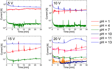 |
| | Fig. 1 Chrono-amperometry results of n-GaN etching in different electrolytes. Current values are normalized to 1 mole of n-GaN. | |
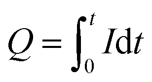
We calculated the number of moles of electrons of n-GaN etching reaction using the connection between total charge of the reaction and concentration of Ga in the electrolyte (eqn (2) and (3)):
| |  | (2) |
| |  | (3) |
Here,
Q (C) is the total charge of
n-GaN etching reaction,
I (A) is the reaction current,
t (s) is the etching time,
z is the number of mols of electrons of reaction,
F is the Faraday constant (96
485 C mol
−1), and
n (mol) is the amount of
n-GaN found in the electrolyte.
ICP-OES data on Ga concentration in the electrolyte during and after the experiments show a close correspondence to z = 6 within the uncertainty of the measurements (Fig. 2 and Table S1, ESI†). At low voltages, the concentration of Ga in the acidic (at 5 V) and neutral (at 5 V and 10 V) solutions during the experiment was lower than the detection limit of this method; this was expected based on the current evolution plots. Nevertheless, we consider that the reaction may develop through various paths at different bias values but within the same number of moles of electrons. Thus, we defined a six-electron nature of n-GaN EC etching process throughout the entire pH range. We previously studied anodic oxidation of n-GaN in oxalic acid and concluded a six-electron nature as well.29 The plots of Ga concentration found by ICP-OES correspond to our discussions on the reaction rates described above.
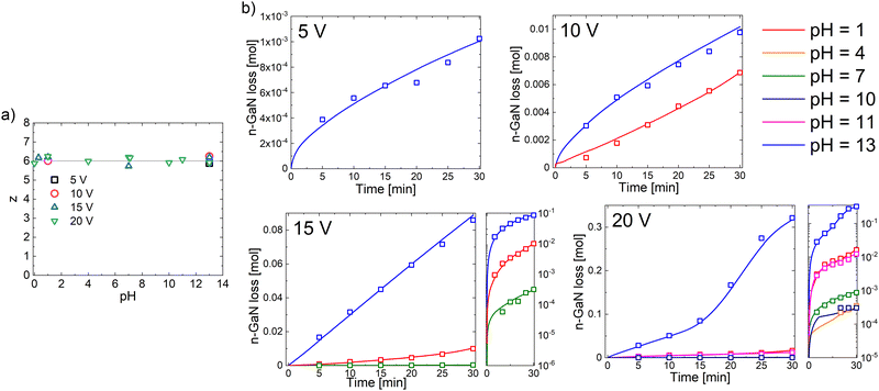 |
| | Fig. 2 (a) Calculations of z from pH 0 to 13, (b, scatters) n-GaN loss measured by ICP-OES and (b, solid lines) estimated from current evolution at z = 6. Values of n-GaN losses are normalized to 1 mole of n-GaN. | |
The vapor phase products of n-GaN electrooxidation were generated on both cathodic and anodic parts. However, their amounts were sufficient for analysis only at 20 V for acidic (0.5 M H2SO4) and alkaline (0.1 M NaOH) electrolytes. Fig. 3 represents the plots of gases generated as the result of n-GaN EC etching reaction. The amounts of hydrogen on the cathode and nitrogen generated on the anode are close to expected values calculated assuming z = 6. We monitored the generation of oxygen on the anode as well, but the amount is not sufficient to consider oxygen as a major reaction product (Table 2). In accordance with the plots of generation of vapor phase products, the reaction was run in diffusion mode for ∼10 min in both acidic and alkaline media. It proceeds in activation mode either until its exhaustion at ∼25 min in H2SO4 or during the remaining time of exposition in NaOH solution.
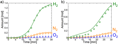 |
| | Fig. 3 (scatters) Amounts of N2 and O2 gases generated on the anode and H2 generated on the cathode at 20 V in (a) 0.5 M H2SO4 and (b) 0.1 M NaOH; (solid lines) amounts of N2 expected on the anode and H2 expected on the cathode according to calculations from reaction currents at z = 6. The amounts of gases generated are normalized to 1 mole of n-GaN. | |
Table 2 Total charges and amounts of reaction products observed
| Electrolyte |
Charge, C |
Ga3+, mmol |
H2(cat), mmol |
N2(an), mmol |
O2(an), mmol |
H2O2, mmol |
| 0.5 M H2SO4 |
1424.1 |
2.44 |
7.02 |
1.04 |
0.26 |
3.81 |
| 1 M Na2SO4 |
284.0 |
0.48 |
— |
— |
— |
0.66 |
| 0.1 M NaOH |
976.4 |
1.73 |
4.84 |
0.78 |
0.38 |
2.26 |
To understand the differences in the reaction mechanisms in various electrolytes, we ran three experiments with similar total charge of the reaction in acidic (0.25 M H2SO4, 15 V), neutral (1 M Na2SO4, 20 V), and alkaline (0.1 M NaOH, 15 V) media. While the rate of etching reaction was the same in alkaline solution, the reaction mode switched from diffusive to activation-controlled in neutral (after ∼10 min) and acidic (after ∼15 min) media (Fig. 4g). SEM images of cross sections and V-pits on the surface of those samples are presented on Fig. 4a–f. The porous structure appears to be branching and current-oriented for all three samples; this is expected at relatively high overpotentials.35 However, the porosification proceeded partially in our case. Nanostructures with a porosity of 18%, 28%, and 25% are formed in acidic, neutral, and alkaline media, respectively. In general, pores with a large average diameter (∼85 nm) are formed in a neutral medium, while an average pore diameter of ∼50 nm was observed after oxidation in sulfuric acid and ∼35 nm was the average pore diameter grown in an alkaline solution (Fig. S1, ESI†). The n-GaN samples were etched from top in acidic and neutral solutions, and the porous nanostructures were distributed throughout the entire sample thickness. Nevertheless, we noticed that the nanoporous structure starts to form from certain points from the top of the surface at 10 V in NaOH (Fig. S2, ESI†). Pores were seen in V-pits after etching in acidic and alkaline electrolytes as seen in the destruction of the V-pit stricture in neutral media. This suggests that threading dislocations are a preferable path for the beginning of n-GaN EC etching reactions.
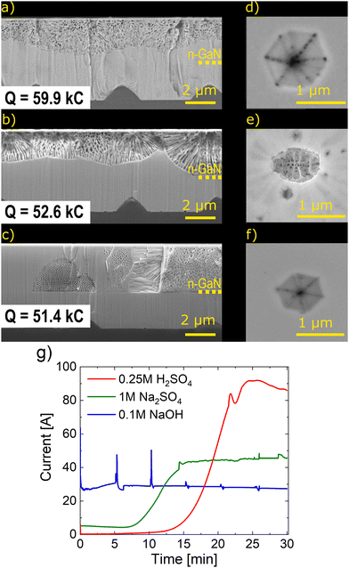 |
| | Fig. 4 (a–c) Cross-section areas of samples after similar total charges passed through n-GaN layers in (a) 0.25 M H2SO4 at 15 V, (b) 1 M Na2SO4 at 20 V, and (c) 0.1 M NaOH at 15 V; (d–f) surface observations of V-pits on the samples etched in (d) 0.25 M H2SO4 at 15 V, (e) 1 M Na2SO4 at 20 V, (f) 0.1 M NaOH at 15 V; (g) chrono-amperometry results of the samples. Values of reaction current are normalized to 1 mole of n-GaN. | |
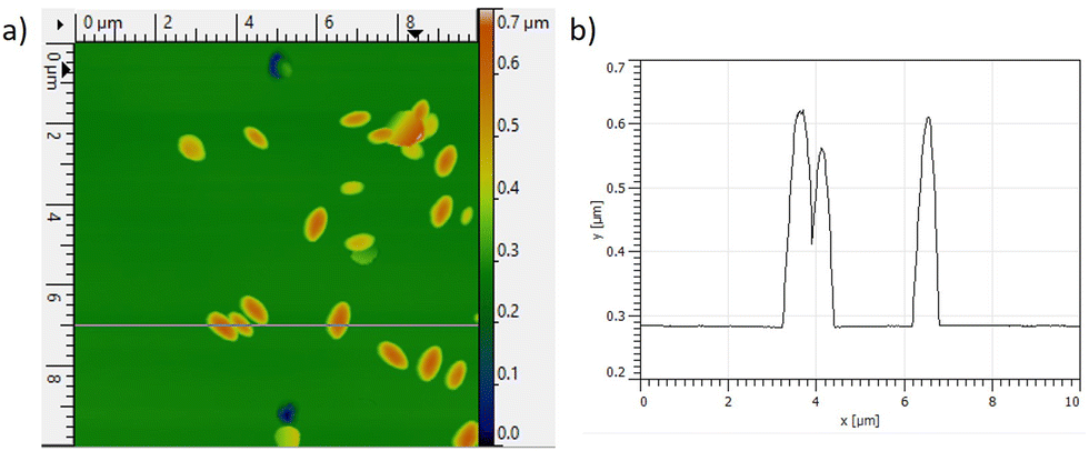
We examined the surfaces of those samples with EDS mapping (Fig. S3–S5, ESI†). There was no oxygen on the surfaces of samples etched in acidic and alkaline media as anticipated.36 However, some grainy particles with high oxygen contents appeared after etching in neutral solution. This is likely the formation of Ga2O3. AFM helped study the sizes and the approximate amount of those particles (Fig. 5a). Ga2O3 particles are 300–600 nm long and ∼300 nm high (Fig. 5b). Considering the observable area, the amount of Ga2O3 is less than 0.4% of the initial amount of n-GaN.
 |
| | Fig. 5 (a) AFM 3D profile of n-GaN surface after etching in 1 M Na2SO4 at 20 V; (b) 1D profile of a corresponding pink line on the 3D profile (left to right). | |
Open circuit potentials in CV measurements were performed in acidic, neutral, and alkaline solutions were −199 mV vs. Ag/AgCl, −248 mV vs. Ag/AgCl, and −346 mV vs. Hg/HgO respectively. We ran the CV experiments in a voltage range of 0–15 V and here we consider the third cycle for comparison as electrocorrosion of the working electrode occurs (Fig. S6, ESI†). According to the obtained voltammograms, the reaction of electrooxidation of n-GaN starts at 4 V in acidic electrolytes while in neutral and alkaline solutions it starts at potentials higher than 2 V. During an increase of the potential we observe an almost linear increment of current from 4 V to 15 V in acids and from 3 V to 15 V in neutral and alkaline media. However, we registered a peak that may be qualified as the formation of nitrogen on a reverse sweep in acidic media. In neutral and alkaline electrolytes, the reverse sweep keeps the reaction current on a static plateau from 15 V to ∼6 V which also may correspond to n-GaN oxidation.
The measurement of Ga concentrations during the experiments as well as the registration of vapor and liquid phase products agree nicely and again illustrate 6 moles of electrons per 1 mole of reaction. Of note, our previous study on etching of n-GaN in oxalic acid29 and the investigations of electrooxidation of n-GaP and n-GaAs come to the same value of z.37 The main difference between etching of n-GaN, n-GaP, and n-GaAs is the oxidation of the solvent in the case of oxidation of n-GaN due to the formation of nitrogen gas. The reaction in solutions of inorganic compounds resulted in water oxidation. The maximum amount of oxygen in anodic gas mixture was found after the process in NaOH: It was 33%, which made it 22% out of the total amount of the products. Thus, oxygen generation is a side path of the n-GaN EC etching reaction in acidic, neutral, and alkaline media. Hydrogen peroxide is the main product of water oxidation. Nitrogen gas is supposed to form due to destruction of a nitride single crystal. The first step of n-GaN EC etching reaction is the formation of a Ga water complex: [Ga(H2O)6]3+ads in acidic and neutral media,38 [Ga(OH)4]−ads in alkaline media.39 This complex adsorbed on a surface of the anode (eqn (4) and (5)). Thus, acidic and neutral solutions proceed as follows:
| | | 2GaN + 12H2O → N2 + 2[Ga(H2O)6]3+ads + 6e− | (4) |
while in alkaline media it starts with
| | | 2GaN + 8OH− → N2 + 2[Ga(OH)4]−ads + 6e− | (5) |
These intermediate surface complexes later decompose with formation of dissolved Ga ions and water oxidation products (
eqn (6)–(10)). We defined the peroxide formation to be a prevailing path of the reaction observed, and thus the decomposition is
| | | 2[Ga(H2O)6]3+ads → 2Ga3+ + 3H2O2 + 6H2O + 6H+ + 6e− | (6) |
or, in alkaline electrolytes,
| | | 2[Ga(OH)4]−ads + OH− → 2Ga3+ + 3HO2− + 3H2O + 6e−. | (7) |
An alternative reaction path results in the generation of oxygen on the anode:
| | | 4[Ga(H2O)6]3+ads → 4Ga3+ + 3O2 + 12H+ + 18H2O + 12e− | (8) |
or
| | | 4[Ga(OH)4]−ads → 4Ga3+ + 3O2 + 4OH− + 6H2O + 12e− | (9) |
depending on the reaction media. Nanoparticles of Ga
2O
3 formed on the surface of sample etched in a solution of Na
2SO
4 because this reaction path realizes less than 0.4% of the total reaction charge:
| | | 4[Ga(H2O)6]3+ads → 2Ga2O3 + 3O2 + 24H+ + 12H2O + 12e−. | (10) |
Thus, the mechanism of the EC etching of n-GaN on the anode involves six moles of electrons—three of these are responsible for a nitride oxidation (eqn (11)), and the remaining three moles of electrons facilitate interaction with the solvent (solv) and form oxidation products (oxd solv) (eqn (12)):
| | | 2GaN + 2n(solv) → N2 + 2[Ga(solv)n]3+ads + 6e− | (11) |
| | | 2[Ga(solv)n]3+ads → 2Ga3+ + 2n(oxd solv) + 6e− | (12) |
Here, a cathode generates the active form of hydrogen ([H*]
ads)
40 (
eqn (13)) that transforms to hydrogen gas on the surface of the Pt wire (
eqn (14)); the hydrogen can also reduces the solvent oxidation products:
29| | | 6H+ + 6e− → 6[H*]ads, | (13) |
Conclusions
We show here anodic etching of n-GaN in various inorganic electrolytes within a voltage range of 5–20 V. Analysis of the reaction products in liquid and vapor phases as well as observations of the nanostructures offer a foundation for detailed description of n-GaN electrooxidation. The etching begins at threading dislocations on the surface of n-GaN layer. The development of n-GaN porous nanostructures depend on the electrolyte; thus, pores spread from the surface and give the solvent access for reaction in acidic and neutral media where the access of the alkaline solvent is less hindered by the double dielectric layer. This permeates via threading dislocations throughout the entire thickness of the n-GaN layer. This reaction involves six moles of electrons for one mole of n-GaN EC decomposition: Three moles of electrons participate in oxidation of water to hydrogen peroxide. This knowledge is critical for a deep detailed understanding of the application and processing of III-nitride materials. The results can lead to high-precision manufacturing of devices based on III-nitride architectures, either for a choice of material to protect ‘artificial photosynthesis’ devices from their corrosion or as a tool to improve the performance of LEDs.
Author contributions
A. S.: investigation, methodology, writing – original draft; D. I.: validation, writing – review & editing; Y. H.: supervision, writing – review & editing; K. O.: conceptualization, project administration, writing – review & editing.
Conflicts of interest
There are no conflicts to declare.
Acknowledgements
This work was financially supported by King Abdullah University of Science and Technology (KAUST) (BAS/1/1676-01-01).
References
-
F. Medjdoub, J.-F. Carlin, M. Gonschorek, E. Feltin, M. A. Py, D. Ducatteau, C. Gaquiere, N. Grandjean and E. Kohn, in 2006 International Electron Devices Meeting, IEEE, 2006, pp. 1–4 Search PubMed.
- B. Imer, F. Wu, M. D. Craven, J. S. Speck and S. P. DenBaars, Jpn. J. Appl. Phys., 2006, 45, 8644 CrossRef CAS.
- D. Maier, M. Alomari, N. Grandjean, J.-F. Carlin, M.-A. Diforte-Poisson, C. Dua, A. Chuvilin, D. Troadec, C. Gaquière and U. Kaiser, IEEE Trans. Device Mater. Reliab., 2010, 10, 427–436 CAS.
- S. Chen and L.-W. Wang, Chem. Mater., 2012, 24, 3659–3666 CrossRef CAS.
- A. R. Acharya, Himalayan Phys., 2014, 5, 22–26 CrossRef.
- S. Nakamura, M. Senoh, N. Iwasa and S. Nagahama, Jpn. J. Appl. Phys., 1995, 34, L797 CrossRef CAS.
- I. Akasaki and H. Amano, Jpn. J. Appl. Phys., 2006, 45, 9001 CrossRef CAS.
- K. Fujii, T. Karasawa and K. Ohkawa, Jpn. J. Appl. Phys., 2005, 44, L543 CrossRef CAS.
- S. Yotsuhashi, M. Deguchi, Y. Zenitani, R. Hinogami, H. Hashiba, Y. Yamada and K. Ohkawa, Appl. Phys. Express, 2011, 4, 117101 CrossRef.
- T. Hayashi, M. Deura and K. Ohkawa, Jpn. J. Appl. Phys., 2012, 51, 112601 CrossRef.
- M. Velazquez-Rizo, D. Iida and K. Ohkawa, Sci. Rep., 2020, 10, 1–9 CrossRef PubMed.
- W. Ohara, D. Uchida, T. Hayashi, M. Deura and K. Ohkawa, Mater. Res. Soc. Symp. Proc., 2012, 1446, 1–9 CrossRef.
- H. Chen, P. Wang, X. Wang, X. Wang, L. Rao, Y. Qian, H. Yin, X. Hou, H. Ye and G. Zhou, Nano Energy, 2021, 83, 105768 CrossRef CAS.
- I. Waki, D. Cohen, R. Lal, U. Mishra, S. P. DenBaars and S. Nakamura, Appl. Phys. Lett., 2007, 91, 93519 CrossRef.
- T. Sekimoto, H. Hashiba, S. Shinagawa, Y. Uetake, M. Deguchi, S. Yotsuhashi and K. Ohkawa, Jpn. J. Appl. Phys., 2016, 55, 88004 CrossRef.
- M. Arunachalam, K. R. Subhash, K. S. Ahn, C. S. Kim, J. S. Ha, S. W. Ryu and S. H. Kang, ACS Appl. Energy Mater., 2022, 5, 2169–2183 CrossRef CAS.
- A. Abdullah, M. A. Johar, A. Waseem, I. V. Bagal, M. A. Hassan, J. K. Lee and S.-W. Ryu, Mater. Sci. Eng., B, 2022, 275, 115514 CrossRef CAS.
- J. H. Ryu, H. Y. Kim, H. K. Kim, Y. S. Katharria, N. Han, J. H. Kang, Y. J. Park, M. Han, B. D. Ryu, K. B. Ko, E.-K. Suh and C.-H. Hong, Opt. Express, 2012, 20, 9999 CrossRef CAS PubMed.
- R. T. Elafandy, J.-H. Kang, C. Mi, T. K. Kim, J. S. Kwak and J. Han, ACS Photonics, 2021, 8, 1041–1047 CrossRef CAS.
- S. S. Pasayat, C. Gupta, Y. Wang, S. P. DenBaars, S. Nakamura, S. Keller and U. K. Mishra, Materials, 2020, 13, 6–15 CrossRef PubMed.
- S. S. Pasayat, C. Gupta, M. S. Wong, R. Ley, M. J. Gordon, S. P. Denbaars, S. Nakamura, S. Keller and U. K. Mishra, Appl. Phys. Express, 2021, 14, 0–4 CAS.
- T. Sugahara, H. Sato, M. Hao, Y. Naoi, S. Kurai, S. Tottori, K. Yamashita, K. Nishino, L. T. Romano and S. Sakai, Jpn. J. Appl. Phys., 1998, 37, L398 CrossRef CAS.
- D.-P. Han, R. Fujiki, R. Takahashi, Y. Ueshima, S. Ueda, W. Lu, M. Iwaya, T. Takeuchi, S. Kamiyama and I. Akasaki, Appl. Phys. Lett., 2021, 118, 21102 CrossRef CAS.
- C. Youtsey, I. Adesida and G. Bulman, Appl. Phys. Lett., 1997, 71, 2151–2153 CrossRef CAS.
- K. Fujii and K. Ohkawa, Phys. Status Solidi C, 2006, 3, 2270–2273 CrossRef CAS.
- M. R. Zhang, F. Hou, Z. G. Wang, S. H. Zhang and G. B. Pan, Appl. Surf. Sci., 2017, 410, 332–335 CrossRef CAS.
- M.-R. Zhang, F.-X. Wang and G.-B. Pan, Electrochem. Commun., 2017, 76, 59–62 CrossRef CAS.
- C. Zhang, G. Yuan, A. Bruch, K. Xiong, H. X. Tang and J. Han, J. Electrochem. Soc., 2018, 165, E513 CrossRef CAS.
- A. Shushanian, D. Iida, Z. Zhuang, Y. Han and K. Ohkawa, RSC Adv., 2022, 12, 4648–4655 RSC.
- S. P. Sundararajan, D. Crouse and Y.-H. Lo, J. Vac. Sci. Technol., B: Microelectron. Nanometer Struct.--Process., Meas., Phenom., 2002, 20, 1339 CrossRef CAS.
- D. Cao, H. Xiao, H. Mao, H. Ma, Q. Gao, J. Liu, J. Ma and X. Liu, J. Alloys Compd., 2015, 652, 200–204 CrossRef CAS.
- S. Wang, L. Zhang, C. Sun, Y. Shao, Y. Wu, J. Lv and X. Hao, Adv. Mater., 2016, 28, 3768–3776 CrossRef CAS PubMed.
- T. Zhu, Y. Liu, T. Ding, W. Y. Fu, J. Jarman, C. X. Ren, R. V. Kumar and R. A. Oliver, Sci. Rep., 2017, 7, 1–8 CrossRef PubMed.
- K. T. P. Lim, C. Deakin, B. Ding, X. Bai, P. Griffin, T. Zhu, R. A. Oliver and D. Credgington, APL Mater., 2019, 7, 021107 CrossRef.
- M. J. Schwab, D. Chen, J. Han and L. D. Pfefferle, J. Phys. Chem. C, 2013, 117, 16890–16895 CrossRef CAS.
- A. N. Hattori, F. Kawamura, M. Yoshimura, Y. Kitaoka, Y. Mori, K. Hattori, H. Daimon and K. Endo, Surf. Sci., 2010, 604, 1247–1253 CrossRef CAS.
- H. Gerischer, J. Vac. Sci. Technol., 1978, 15, 1422–1428 CrossRef CAS.
- W. W. Rudolph and C. C. Pye, Phys. Chem. Chem. Phys., 2002, 4, 4319–4327 RSC.
-
A. J. Downs, Chemistry of aluminium, gallium, indium and thallium, Springer Science & Business Media, 1993 Search PubMed.
- Y. B. Vassiliev, V. S. Bagotzky, N. V. Osetrova and A. A. Mikhailova, J. Electroanal. Chem., 1985, 189, 311–324 CrossRef.
Footnote |
| † Electronic supplementary information (ESI) available: Details of pores observations, EDS mapping and cyclic voltammetry of the samples. See DOI: https://doi.org/10.1039/d2nj04740c |
|
| This journal is © The Royal Society of Chemistry and the Centre National de la Recherche Scientifique 2022 |
Click here to see how this site uses Cookies. View our privacy policy here. 
 Open Access Article
 This Open Access Article is licensed under a
  a,
Daisuke
Iida
a,
Daisuke
Iida