
 Open Access Article
 This Open Access Article is licensed under a Creative Commons Attribution-Non Commercial 3.0 Unported Licence
Total electrification of large-scale nanophotonic arrays by frictional charges†
Nikhil
Bhalla
 *ab,
Zidong
Yu
c,
Serene
Pauly
d,
Amit
Kumar
d,
Chiranjeevi
Maddi
a,
Davide
Mariotti
a,
Pengfei
Zhao
e,
Amir Farokh
Payam
ab and
Navneet
Soin
*a
*ab,
Zidong
Yu
c,
Serene
Pauly
d,
Amit
Kumar
d,
Chiranjeevi
Maddi
a,
Davide
Mariotti
a,
Pengfei
Zhao
e,
Amir Farokh
Payam
ab and
Navneet
Soin
*a
aNanotechnology and Integrated Bioengineering Centre (NIBEC), School of Engineering, Ulster University, Shore Road, BT37 0QB Jordanstown, Northern Ireland, UK. E-mail: n.bhalla@ulster.ac.uk; n.soin@ulster.ac.uk
bHealthcare Technology Hub, Ulster University, Shore Road, BT37 0QB Jordanstown, Northern Ireland, UK
cInstitute for Materials Research and Innovation (IMRI), School of Engineering, University of Bolton, Bolton BL3 5AB, UK
dSchool of Mathematics and Physics, Queen's University Belfast, University Road, Belfast BT7 1NN, Northern Ireland, UK
eDepartment of Precision Mechanical Engineering, Shanghai University, Shanghai 200444, P. R. China
First published on 22nd September 2022
Abstract
Localized surface plasmon resonance (LSPR) of metallic nanostructures is a unique phenomenon that controls the light in sub-wavelength volumes and enhances the light–matter interactions. Traditionally, the excitation and measurement of LSPR require bulky external light sources, and efforts to scale down to nano-plasmonic devices have predominantly relied on the system's miniaturization and associated accessories. Addressing this, here we show the generation and detection of LSPR wavelength (λLSPR) shifts in large-area nanostructured Au surfaces using frictional charges generated by triboelectric surfaces. We observe a complex interplay of the localized surface plasmons with frictional charges via concurrent spectroscopic and triboelectric measurements undertaken for the detection of bioconjugation in the streptavidin–biotin complex. When subjected to multivariate principal component analysis, a strong correlation between the triboelectric peak-to-peak voltage output response and the λLSPR shift is observed. Furthermore, we reveal a landscape of the interfacial events involved in the electrical generation/detection of the LSPR by using theoretical models and surface characterization. The demonstrated concept of electrification of plasmon resonance thus provides the underlying basis for the subsequent development of self-powered nano-plasmonic sensors and opens new horizons for advanced nanophotonic applications.
New conceptsTraditionally, a physical light source and a spectrophotometer are required for the generation and detection of localised surface plasmon resonances (LSPR) from large-scale arrays of nanoplasmonic particles. Here, we establish new concepts to detect and generate LSPR without the use of light source and any external power supply. We achieve this by utilising the nanoscale triboelectric charge generating (via friction) structures to provide energy for plasmon generation at the metal-insulator junctions. The same charge generators are used for detecting the LSPR associated with the large-area metal nanostructured substrates, as they are placed in the feedback loop of the self-powered electrical system. In simple words, one can visualise our whole work resulting in the generation and detection of surface plasmons by simply rubbing two nanoscale objects. In this process, we also discover slow discharge of surface potential created by surface polaritons, found in the timescale of few minutes in our work, on the nanostructures. This is completely unexpected and surprising finding as it is well known that plasmons have a lifetime of picoseconds. |
Introduction
Nano-plasmonic sensors have been investigated extensively to develop applications in point-of-care diagnostics,1 drug discovery,2 environmental monitoring,3 and food safety4 amongst others. For realizing these nano-plasmonic sensors, bulky light sources and a suite of accessories including lasers, fibers, lenses, etc., impose a significant power requirement while limiting their miniaturization. The current state of the art in the on-chip generation of plasmons either through the direct electronic–plasmonic transducers5 or via indirect electrical plasmon sources6 involves inherently slow electron–hole recombination (picosecond range) as compared to the femtosecond timescale achieved in mechanical tunnelling effects. The recent realization of electrically excitable surface plasmon polaritons in Metal–Insulator–Metal (MIM) tunnelling junctions has opened a pathway to develop sub-diffraction limit devices that can achieve ultrafast light emission by inelastic tunnelling and thus can ‘electrify’ plasmons.7,8 Nonetheless, these developments are yet to transform nano-plasmonic sensors into self-powered, light-source-free sensing set-ups. The reasons underpinning this are primarily associated with the challenges of integrating the light-trapping and electromagnetic-field concentrating properties of plasmons, with materials that can concurrently provide suitable energy-harvesting pathways. For instance, it is non-trivial to directly integrate advanced materials such as graphene9 or metamaterials,10 which have the potential to electrify plasmons for realising devices in self-powered formats for real-world sensing applications.At the same time, ubiquitous biosensing systems are being pursued for increasingly demanding real-time healthcare and diagnostic applications.11 In this aspect, one long championed sensitive biosensing technique suitable for the measurement of biomolecule binding events on solid surfaces is surface plasmon resonance (SPR) – whose manifestation in nanoparticles is commonly termed localized surface plasmon resonance (LSPR). It usually involves the use of a light source and a spectrometer alongside connecting fiber optics and the technique measures changes in the refractive index of the surrounding medium upon binding of a biomolecule which is then identified as a wavelength shift or a change in the peak intensity. The benefits of compact sensing volume and the inherent label-free detection are further helped by the stability of the LSPR as it focuses on the measurement of spectral shifts and is thus relatively immune to environmental noise as compared to its contemporary transduction methods for biosensing.12 Nevertheless, the possible elimination of external light sources for LSPR excitation and power source for plasmonic signal acquisition could eventually lead to ultra-compact electrically addressable on-demand biosensors. Especially technologies enabling such self-powered biosensing operating without an external electronic power source or onboard battery13 can provide a low-cost accurate diagnostic platform for resource-limited countries which is free from infrastructure constraints. The typical reports on the self-powered biosensors describe the use of either photovoltaics,14 enzymatic reaction,15 or more recently, triboelectric (electrostatics),16 to supply power. For triboelectric devices, photo-stimulation for charge density control has been demonstrated earlier in low-bandgap halide semiconductors17 and perovskites,18 however, utilisation of plasmonic effects has not been demonstrated widely, barring in Au/TiO2 triboelectric nanogenerators (TENGs), which requires UV excitation owing to the large bandgap in TiO2 (∼3.2 eV).19
Our work demonstrates the pathway towards the generation and detection of LSPR from a large-scale array of nanophotonic structures using photo-enhanced frictional charges generated upon the instantaneous interfacial interaction of Au nanoparticles (on indium tin oxide (ITO)) and polydimethylsiloxane (PDMS)/ITO surfaces. Essentially, we utilise the Au and PDMS as triboelectric materials to generate frictional charges, which then tunnel through the metal conducting metal-oxide junction consisting of an array of Au nanoparticles on a transparent conducting oxide (ITO). The charges tunnel through the instantaneous interface of Au leading to the electrical output of the TENG system in the form of the electrical current. This electrical output is correlated with the LSPR wavelength shifts. We show that these changes in the charge density correspond to the fingerprints of the LSPR of Au nanostructures by concurrent optical and electrical measurements (see Fig. 1).
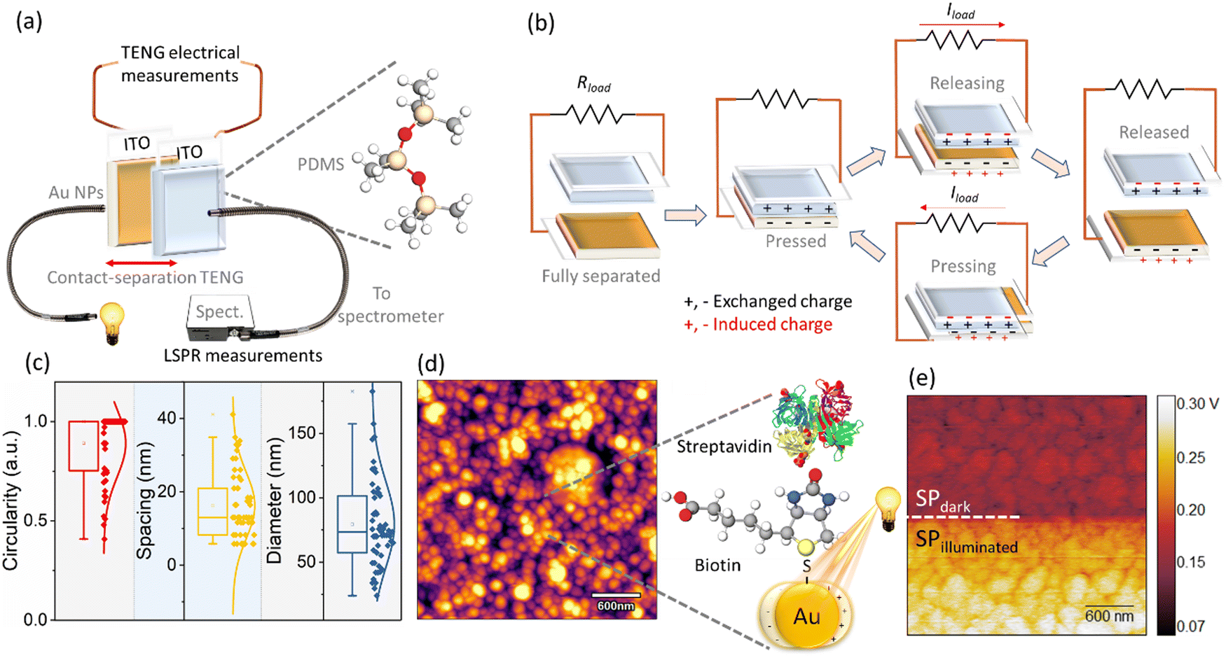 | ||
| Fig. 1 Sensor topography and detection scheme: (a) schematic for the concurrent LSPR and triboelectric measurements employing Au/ITO against PDMS/ITO substrates. (b) Operating principle of TENG measurements under short circuit conditions. The annealing of Au thin films (deposited on ITO) gives rise to typical spherical morphology with (c) the corresponding statistical measurements on the Au nanoparticles of their circularity (mean 0.89), spacing (16.3 nm), and diameter (79.3 nm) obtained from ImageJ analysis of (d) the tapping mode AFM images of Au/ITO substrate. The Au/ITO substrates are initially functionalized using biotin and subsequently, its conjugation with streptavidin is measured via the concurrent LSPR and TENG measurements (shown in (a)). (e) Fundamental KPFM measurements on the Au/ITO substrates highlight the significant variation in the surface potential arising from plasmo-electric and hot-electron injection effects under illumination. | ||
Our experimental setup performs the following tasks: (i) exposing the triboelectric system to isolate the effect of light in the electrical (peak-to-peak voltage, current, and charge density) measurements and (ii) measuring the plasmon generation optically via the portable spectrophotometer. Interestingly, statistically insignificant variance in the electrical parameters of peak-to-peak voltage (Vp–p) was observed in the triboelectric response of the system in the presence and absence of the light source, whilst the spectrometer successfully recorded the LSPR spectrum. This suggests that changes in the electrical signals, obtained from the triboelectric measurements did contain signatures of plasmon generation and detection. Motivated by these findings, we extended our discovery to develop a simple biosensor by studying the bioconjugation of biotin and streptavidin. Both, the electrical and optical response of the system was acquired, and the data generated was further analyzed using principal component analysis (PCA). The PCA by virtue of its dimensionality-reduction aspect transforms a large set of variables (with no apparent relationship) into a smaller set that still preserves the information of the large dataset.20 Based on this analysis, a statistically significant correlation between the electrical parameters including the Vp–p and the optical LSPR wavelength shifts, λLSPR, was observed (dependent on the concentration of streptavidin). Thus, the reported concurrent optical and electrical measurements, for which the Vp–p provides a reliable measure of the λLSPR and therefore the analyte concentration, provide the framework for the development of electrically enabled self-powered plasmonic-based sensors.
Results and discussion
Before undertaking the bio-conjugation measurements, to understand the role of LSPR in modulating the electrical response, the TENG electrical measurements of pristine Au/ITO against PDMS/ITO were carried out under dark and illuminated conditions (Fig. 2(a)). Under a 50 N (5 Hz) cyclical impact, the pristine Au-PDMS TENG produced a peak-to-peak voltage in dark (Vp–p, dark) of ∼215.0 ± 7.0 Vp–p, which under illumination increased to ∼229.0 ± 8.5 (Vp–p,light). Accordingly, the charge densities showed a slight but consistent increase from σdark ∼ 112.0 ± 3.4 μC m−2 to σlight ∼ 115.0 ± 3.4 μC m−2, respectively (Fig. 2(e), “Au”). As compared to PDMS – a tribo-negative material, Au is relatively positive in the triboelectric series, which upon illumination sees a further rise in its surface potential which then promotes a larger charge exchange (discussed later).21 Upon the subsequent functionalization of the Au-substrate with biotin, a significant change in the electrical response was observed with a voltage output of ∼275.0 ± 6.2 Vp–p,light (Fig. 2(b)). This was also accompanied by an increase in the current density from Jsc,dark of 80.5 ± 5.19 mA m−2 to Jsc,light of 84.9 ± 3.04 mA m−2 (Fig. 2(c)) and charge density of (σdark ∼ 116.6 ± 4.15 μC m−2 to σlight ∼ 127.0 ± 2.28 μC m−2 under illumination), respectively (Fig. 2(e), “Biotin”). It is understood from literature that nitrogen-functional groups including amide develop the most positive charge (0.5–1.2 pC cm−2), followed by the oxygen functional groups (0.6–1.1 pC cm−2).22,23 Thus, the enhancement of electrical response after the addition of a small molecule such as biotin (with functional amide and carboxylic groups) on Au/ITO substrates can be fully explained. The typical optical spectrum of LSPR with absorbance vs. wavelength (λLSPR) shows an average blue shift of 6.34 nm (from 605.50 nm to 599.16 nm) and an increase in absorbance (area under the curve) upon the attachment of biotin on the surface of the sensor, see also statistical data for multiple replicates (n = 6, Fig. 3(a) and (b)). The addition of the analyte, streptavidin, leads to a strong and specific noncovalent interaction with biotin, leading to the formation of a high-affinity complex (dissociation constant, Kd = 10−15 M−1)24 which is then reflected in the variation of the LSPR and TENG electrical output.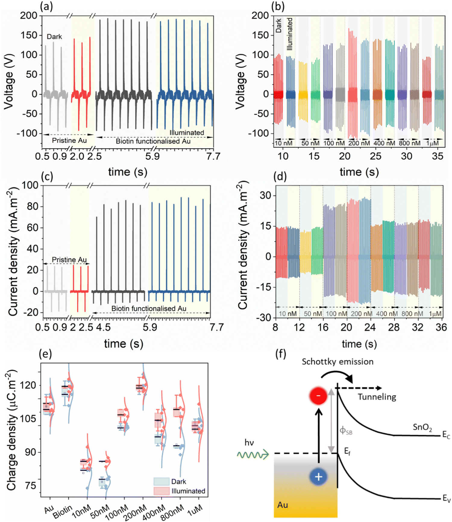 | ||
| Fig. 2 Electrical measurement results of the Au/PDMS TENG (50 N force, 5 Hz frequency) at various stages. (a) The voltage response of pristine Au/PDMS and biotin-functionalized Au/PDMS under dark and illuminated conditions, with their corresponding (c) output current density. The effect of streptavidin addition (10 nM–1 μM) and subsequent conjugation with biotin is visualised in the (b) voltage and (d) current response of the streptavidin–biotin Au/PDMS TENG, respectively. (e) A clear change in the charge density (under dark and illuminated conditions) was observed for the Au/PDMS TENG at different experimental stages. (f) The LSPR excited by incoming photons results in photoexcited hot-electrons which depending on their energy either tunnel to the SnO2 or undergo Schottky emission over the barrier (φSB). | ||
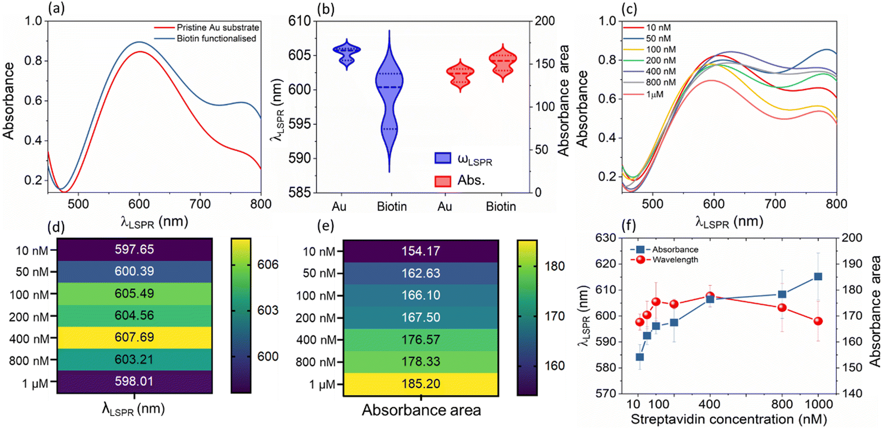 | ||
| Fig. 3 (a) Typical LSPR spectrum representing wavelength vs. absorbance plot for (unfunctionalized) and biotin functionalized LSPR substrate; (b) wavelength and absorbance changes of the sensor upon attachment of biotin on the sensor surface; (c) LSPR spectrum of wavelength vs. absorbance change of the sensor upon exposure to streptavidin of concentrations ranging from 10 nM to 1 mM; heat map of (d) peak wavelength changes of the sensor and (e) absorbance area changes of the sensor upon exposure to streptavidin of concentrations ranging from 10 nm to 1 mM; and (f) LSPR wavelength and absorbance area shifts plotted on a linear scale (n = 4, n refers to the number of replicates for each point). | ||
The variation shown in Fig. 3(c) upon the binding of streptavidin (1 mM to 10 nM) to biotin leads to an increase in the mean λLSPR and absorbance area of the LSPR spectrum, see Fig. 3(d) and (e) for λLSPR and absorbance changes, respectively. Note that we only monitor shifts in the peak between 500 and 700 nm. Usually, an increase in the peak wavelength (redshift) and absorbance in the LSPR spectrum are observed upon binding of a given biomolecule on the sensor surface due to an increase in the dielectric constant from biomolecule mass addition.25 Whilst the absorbance increases with the biotin–streptavidin binding (i.e., increase in streptavidin concentration), the wavelength decreases (blueshifts) for the biotin-binding and binding of concentrations of the streptavidin above 400 nM. This is attributed to the dominance of the charge on the sensor surface from the biotin and streptavidin molecules (Fig. 3(f)); this charge effect masks the effect of mass binding on the surface of the nanostructures, as also observed in our previous works for other analyte bindings.26,27 Additionally, the increase in the charge density upon binding of streptavidin discussed earlier in Fig. 2(b) and (d), also indicates that charge effects lead to blue shifts. For instance, both the voltage and current density showed an abrupt increase at 100 nM loadings, which was also reflected in the LSPR absorbance area measurements in the same concentration range.
To understand this complex variation of the electrical and optical data, we performed principal component analysis (PCA). Essentially, we find the relationship between the five different parameters (variables) of the sensor response to the binding of streptavidin with biotin: λLSPR shifts and absorbance area from the absorbance measurements and the peak-to-peak voltage (Vp–p,light), and charge densities, σdark and σlight, from the electrical measurements. The method used to select the principal components is based on the Kaiser–Guttman rule, which allows us to consider all principal components with eigenvalues greater than 1. From Fig. 4(a), it can be observed that there are 2 principal components, PC1, and PC2, which have eigenvalues greater than 1 and together they account for 83.41% of the variance in the data, see Fig. 4(b), and are therefore used for further analysis. It should be noted that these principal components themselves are given by a linear combination of the input variables, where the weighting coefficients are called loadings. Fig. 4(c) shows the loadings plot which highlights the groupings between the five optical and electrical parameters using the two principal components, PC1, and PC2. The points which lie closer to each other in the loading plot are considered to be closely related parameters. More specifically, if two points lie on a given vector, we can consider one of these points as completely redundant to describe the behaviour of the analysed system. The plot in Fig. 4(c) indicates that the optical LSPR wavelength shift, λLSPR, and TENG electrical output, Vp–p light, are closely related to each other, indicating that the λLSPR changes are proportional to the changes in the Vp–p. In contrast, the absorbance area of the sensor response is relatively independent as compared to σlight–σdark and λLSPR–Vp–p pairs. We also show the principal components scores where PC1 is represented on the x-axis and PC2 on the y-axis, see Fig. 4(d). These PC scores, calculated using linear combinations that define each PC in terms of the variables, allow for the projection of the original value of the variables into the two-dimensional space defined by the two selected PCs. The biplot of loadings and PC scores has the same axis scale as that of the PC scores in Fig. 4(c), whilst loadings are scaled (90% of PC scores) within this new axis. This implies that the angles of the vectors can be interpreted in the same manner as in the loadings plot, however, the coordinates of these vectors cannot be compared. Note that this biplot is just a visualization of results by combing loadings and PC scores. To corroborate the PCA results, we have also analysed our data with alternative methodologies. Fig. 4(e) shows a multiple variable bubble plot showing the relationship between Vp–p and LSPR wavelength, and the Pearson correlation is plotted in the heat map, see Fig. 4(f). From this heat map, we can observe a linear trend between Vp–p and λLSPR which have an r2 value of 0.82 according to the Pearson correlation matrix, indicating a significant relationship between Vp–p and LSPR wavelength in comparison with other relationships of Vp–p with σlight (r2 = 0.38), σlight (r2 = 0.40) and absorbance (r2 = −0.13). It is understood that for conventional LSPR sensors, the λLSPR shift is characteristic of the concentration of the analyte as well as the strength of binding.26,27 At the same time, changes in the electrical output of the TENGs for use as a sensor for label-free detection of analytes have been shown,28,29 however, no studies so far reported on the concurrent LSPR-TENG measurements. By establishing this strong correlation between the λLSPR shift of the LSPR component and the Vp–p response of the TENGs, the pathway to establishing self-powered LSPR-based sensors has been opened.
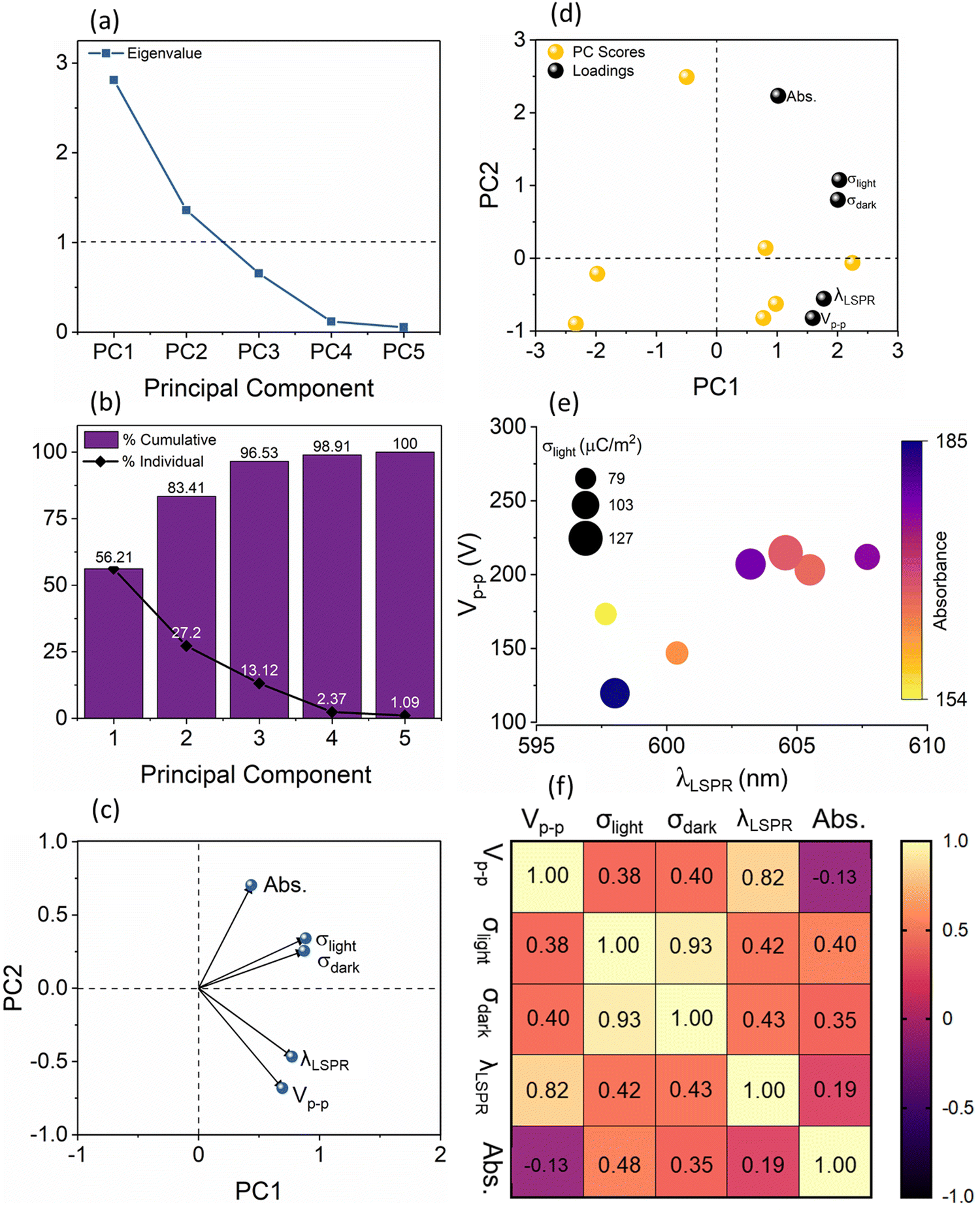 | ||
| Fig. 4 (a) Eigenvalues for different principal components; (b) bar graph representing cumulative variance, in percentage, associated with principal components; (c) loadings plot showing the relationship between the variables; (d) biplot of loadings and PC scores (depicting the relationship between original data and selected principal components (PC1 and PC2)) for the visualisation of the original dataset and principal components; (e) bubble plot showing the relationship between the Vp–p and LSPR wavelength and absorbance for streptavidin binding and (f) correlation matrix showing Pearson correlation coefficient (two-tailed test with a confidence interval of 99%) between the sensor variables. | ||
To elucidate the physical phenomena occurring at the interface of Au and ITO, we have performed light-modulated Kelvin Probe Force Microscopy (KPFM) measurements of the pristine Au/ITO samples, XPS, and physical modelling of the interfacial thickness. Using KPFM, we measure the differences in surface potential of Au/ITO under dark and illuminated conditions to account for the charge density differences observed under light and dark modes of the electrical measurements using TENG as shown earlier in Fig. 2, and co-related using PCA analysis in Fig. 4(c). Fig. 5(a) and (b) shows the acquired KPFM image and the corresponding surface potential distribution on the Au/ITO surface, while the intensity of light was modulated during the real-time scanning process. For the 4 × 4 μm2 images, the sample was kept in dark for the first portion of the acquisition (∼1 μm) at which point, the sample was illuminated at 30%, 50%, and eventually 100% of the maximum illumination for a certain duration (as highlighted by the dotted lines). A representative histogram of the extracted surface potential from Fig. 5(a) is presented in Fig. 5(b). Under dark conditions, an average surface potential value of ∼280 mV was observed which verifies the triboelectric positive nature of the sample, while an increase in this surface potential to ∼425 mV was observed for the fully illuminated Au-ITO sample. This positive shift of ∼145 mV, arising from ΔSP = SPilluminated − SPdark, where SPilluminated and SPdark correspond to the surface potential in illuminated and dark states, respectively, can be attributed to the combined effect of the formation of plasmo-electric potential in metal nanostructures as previously described by Sheldon et al.30 and LSPR field enhancement.31 The plasmo-electric potential is defined as the formation of an electrostatic potential owing to an optically driven change in the carrier density of plasmonic nanostructures and is illumination wavelength (λillumination) dependent.30,32 As such an inherent asymmetry exists wherein a negative plasmo-electric potential corresponding to a reduction in the surface potential arises from the enhanced carrier density (for λillumination < λLSPR), while for λillumination > λLSPR, a positive plasmoelectric potential and enhanced surface potential is observed.30,32 For the Au/ITO substrates (with λLSPR ∼ 600 nm), the broad wavelength spectrum of the applied white light (see Fig. S1, ESI†) induces an upshift of the surface potential, which is indicative that wrt to the negative tip, the electronic charge exits the grounded Au/ITO substrate.17,32 This is aided by the difference in the Fermi levels between the Au and ITO, which leads to the formation of a relatively small barrier height (φSB ∼ 0.7 eV). This allows the injection of hot electrons into the ITO substrate and thus leaves the Au positively charged owing to electronic depletion.19 This charge transfer direction for Au nanoparticles with a specific λLSPR observed in our experiments is consistent with the thermodynamic model proposed by Sheldon et al.,30 see more detailed explanation in the ESI† (Fig. S2).
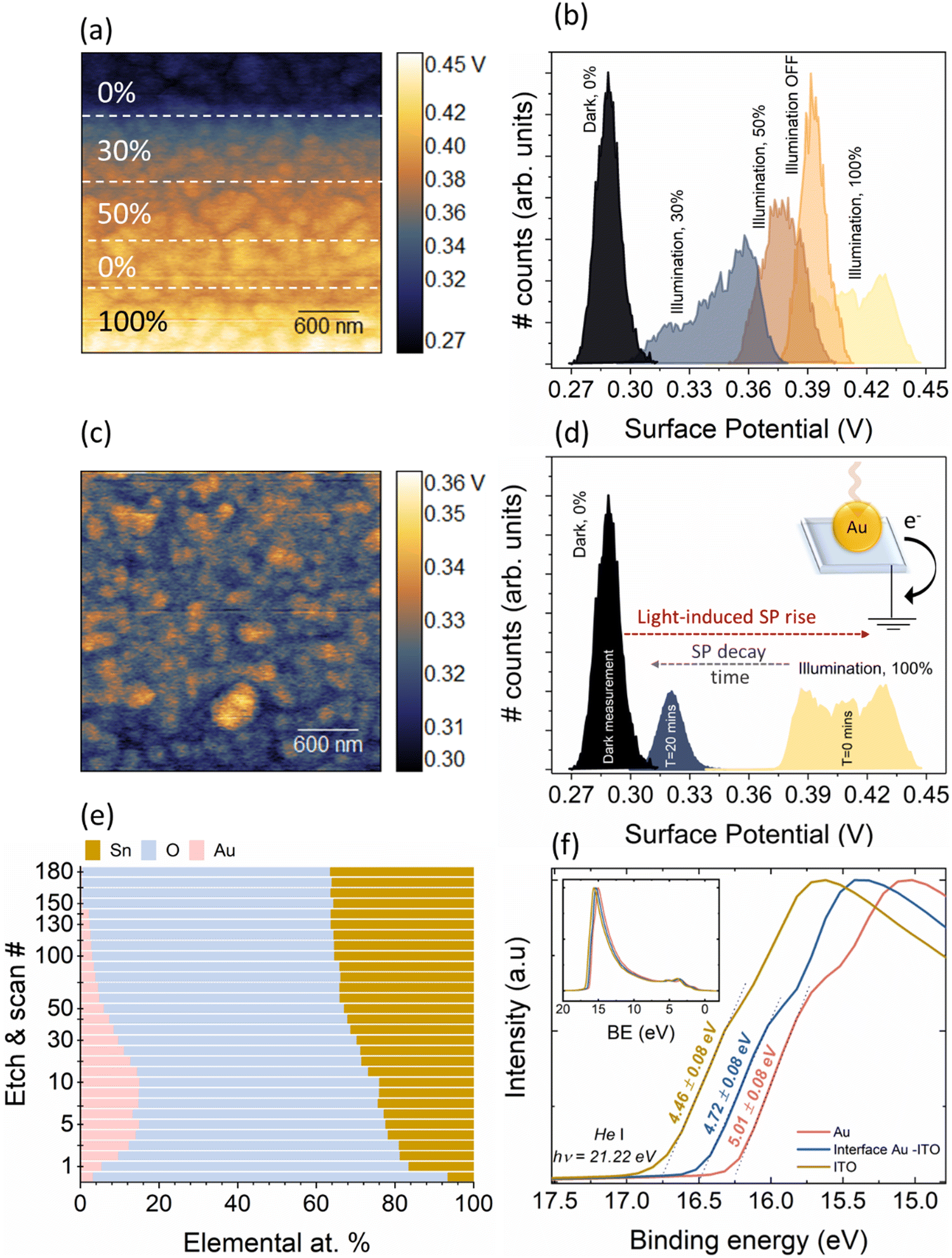 | ||
| Fig. 5 (a) KPFM surface potential images of pristine Au/ITO substrate under varying illumination conditions, starting from dark (0% illumination), which was then varied to 30%, 50%, 0%, and finally to full brightness (100% illumination), while (b) shows the corresponding surface potential histograms under these conditions wherein a clear increase with illumination was observed. Considering the time at the end of the scan (at 100% illumination) as T = 0, the (c) surface potential decay was measured after T = 20 min, with the corresponding histogram in (d), which highlights the relatively slow decay of potential. (e) XPS depth profiling of the Au/ITO system with the elemental composition corresponding to Au, O and Sn (in at%). (f) He–I UPS measurements show the depth-profile dependent variation of the work function/ionization energy of the Au/ITO structure. | ||
From Fig. 5(c) and (d), upon illumination, a fast-rising, significant increase in the SP (see Fig. S4 and associated discussion and calculations in ESI†) was observed, however, when the illumination was switched off, the increased SP did not immediately return to its original value. The SP displayed a relatively slow decay, and even 20 minutes after switching OFF the illumination, a marginally higher SP of ∼300 mV could be observed as compared to the original measurement in the dark of ∼280 mV (see Fig. S3 for longer timescales, ESI†). This observed slow SP decay can have multiple origins ranging from uncompensated charges with long lifetimes, to charge exchange with the ambient which is influenced via a screening effect through the formation of a water layer or from the presence of a charge-trapping layer and/or a wider Au/ITO Schottky-type interface.17,19 To probe this further, we have conducted depth-profiling XPS measurements using low-energy monoatomic Ar+ sputtering with an average sputtering rate of 1.7 Å per step. Fig. 5(e) shows the elemental variation as a function of sputtering cycles. Starting from step 1 to step 10, progressively strong Au 4f signals commensurate with metallic Au were observed (Fig. S5, ESI†). Corresponding to the levels of interest (Au-dominant, interface, and substrate-dominant), the He–I UPS measurements at these depths clearly shows the presence of a barrier (φ ∼ 0.55 eV, Fig. 5(f)). We also theoretically modelled the interfacial thickness of this Au/ITO Schottky-type interface (Table S1, ESI†). The model utilizes a metallic sphere-insulator-metallic film-based MIM capacitive structure where a single Au nanoisland of the LSPR substrate is considered as a sphere, the Schottky-type interface as the dielectric of the capacitor, and ITO as the metallic film (see ESI†). Within this model, we use the charge distribution obtained from the KPFM for modelling the apparent capacitance behaviour which revealed an interfacial thickness of 1–1.2 nm for the wide Schottky barrier. This length is appropriate to facilitate electron tunnelling between Au and ITO which assists in the formation of plasmons at the metal/insulator interface.
In summary, we have demonstrated an explicit relationship between the LSPR wavelength shifts and the electrical output of a triboelectric charge generation system. This principle can potentially be harnessed to develop innovative devices with revolutionary applications in the future. For instance, we foresee self-powered wireless motion sensors for use in bedside patient care, point-of-care devices, prosthetic devices, and lifestyle-monitoring gadgets such as those suitable for installation in smart homes for elderly care could be developed at a low cost and with improved sensitivity. In addition, it opens the door for ultra-sensitive plasmonic-based bio/chemical sensors, to detect biomolecule binding and affinity kinetics, for their translation into wearable/flexible electronics. Self-powered quantum antennas, which are yet to be realized, could well be developed by utilisation of the combinatorial interplay of photonic and frictional charges demonstrated in this work. Our future works will consider the establishment of a stronger correlation between the observed electrical generation/detection (by TENGs) and optical modulation of LSPR (of Au nanoparticles) via control over the nanoparticle size/distribution which limits the higher order modes. On a similar basis, other optical systems which require light sources and spectrophotometers, such as SERS and surface-enhanced infrared absorption (SEIRA)33–38 can potentially be electrified. Therefore, our work serves as a benchmark for the electrification of optical systems using TENGs in a self-powered manner. This will certainly enlarge the boundaries of the application of photonic devices, many of which are yet to be discovered.
Methods
Reagents
Biotin, ≥99% (HPLC grade) lyophilized powder, and salt-free Streptavidin lyophilized powder, ≥13 units per mg were purchased from Sigma Aldrich, UK. PDMS prepolymer (Sylgard 184A) and cross-linker agent (Sylgard 184B) were purchased from Dow Corning. ITO-coated glass slides with resistivity ∼8–10 Ω sq−1 were obtained from Sigma Aldrich, UK. The Au-ITO substrate, prepared by magnetron sputtering, was obtained commercially from NanoSPR LLC, USA.Fabrication and integrated LSPR-TENG measurements
As seen in the schematic (Fig. 1), the biotin–Au/ITO and PDMS/ITO substrates were used as the tribo-positive and tribo-negative electrodes, respectively. The PDMS pre-polymer and cross-linking agents, taken in a 10![[thin space (1/6-em)]](https://www.rsc.org/images/entities/char_2009.gif) :1 ratio was stirred, degassed and then spin-coated (500 rpm for 5 s, followed by 2000 rpm for 10 s; deposition area of 20 × 20 mm2) on clean ITO substrates. The as-prepared PDMS/ITO was then cured for 60 min in an oven (100 °C) to obtain continuous ∼75 μm thick films (Fig. S7, ESI†). A computer-controlled dynamic fatigue tester system was used to characterize the electrical output of TENG under a fixed impact force of 50 N, a frequency of 5 Hz, and a separation distance of 5 mm. An oscilloscope (Tektronix MDO3022, connected via a 100 MΩ input impedance high accuracy, high voltage passive probe) and picoammeter (Keysight B2981A) were connected in series or parallel to the external circuit of TENG to measure the output current and voltage, respectively. The output charge density was derived by calculating the area under the curve of the measured current density in one contact-separation period.17 For all the TENG output measurements, the electrode on the biotin–Au/ITO was connected to the positive lead, while the electrode on the PDMS side was grounded. The concurrent LSPR measurements are acquired using an in-laboratory-built optical instrument comprising a FLAME-T-XR1-ES spectrometer (Ocean Optics), UV-Vis patch connectors, DH-2000 deuterium–tungsten halogen lamp (DH 2000-S-DUV-TTL), RTL-T stage, and Ocean View software. Before the acquisition of the LSPR spectrum, dark and reference signals for background noise cancellation were measured using a bare ITO slide (like the ones on which Au nanostructures were deposited) as the reference.
:1 ratio was stirred, degassed and then spin-coated (500 rpm for 5 s, followed by 2000 rpm for 10 s; deposition area of 20 × 20 mm2) on clean ITO substrates. The as-prepared PDMS/ITO was then cured for 60 min in an oven (100 °C) to obtain continuous ∼75 μm thick films (Fig. S7, ESI†). A computer-controlled dynamic fatigue tester system was used to characterize the electrical output of TENG under a fixed impact force of 50 N, a frequency of 5 Hz, and a separation distance of 5 mm. An oscilloscope (Tektronix MDO3022, connected via a 100 MΩ input impedance high accuracy, high voltage passive probe) and picoammeter (Keysight B2981A) were connected in series or parallel to the external circuit of TENG to measure the output current and voltage, respectively. The output charge density was derived by calculating the area under the curve of the measured current density in one contact-separation period.17 For all the TENG output measurements, the electrode on the biotin–Au/ITO was connected to the positive lead, while the electrode on the PDMS side was grounded. The concurrent LSPR measurements are acquired using an in-laboratory-built optical instrument comprising a FLAME-T-XR1-ES spectrometer (Ocean Optics), UV-Vis patch connectors, DH-2000 deuterium–tungsten halogen lamp (DH 2000-S-DUV-TTL), RTL-T stage, and Ocean View software. Before the acquisition of the LSPR spectrum, dark and reference signals for background noise cancellation were measured using a bare ITO slide (like the ones on which Au nanostructures were deposited) as the reference.
Bioassay
Essentially, we measured the TENG/LSPR signals at 3 different surface states of the substrate: un-functionalized pristine Au substrate (stored before use at 4 °C in dark); after biotin functionalization; and after the biotin–streptavidin complex formation upon exposure to different concentrations (ranging from 10 nM to 1 mM) of streptavidin. Note that the buffer used for the preparation of both biotin and streptavidin solutions was phosphate buffer saline (PBS) solution (0.01 M, 7.4 pH). The biotin functionalization was performed using drop-casting of 50 ml of 1 mg ml−1 biotin solution on the sensor surface. After drop-casting, the sensor surface was incubated in a humidified chamber to avoid evaporation of the solution. Thereafter, the sensor surface was washed with PBS, and gently dried with nitrogen and at this stage, TENG/LSPR spectrum was immediately acquired for a biotin functionalized sensor state. The biotin-functionalized sensor was then exposed to the various concentrations of streptavidin. After 15 minutes of incubation in a humidified chamber, TENG/LSPR response was recorded post-washing with PBS and gentle drying with compressed nitrogen.PCA and statistical analysis
We use a classical method based on the Kaiser–Guttman rule (also known as the Kaiser criterion) to select principal components (PC). For dimensionality-reduction PCA analysis, we have considered the electrical output characteristics of Vp–p, σlight, and σdark (covering the illuminated and dark conditions, respectively) and the optical characteristics of λLSPR and absorbance. Each of the principal components (linear combination/mixture of starting variables) is uncorrelated and the information from the initial variables is compressed into these via orthogonal eigenvectors that represent the maximal amount of variance in dataset.39 Thus, the PCA essentially extracts the smallest number of components that describe the most variation of the original dataset with minimal loss of information. In this method, we assume that with the standardized data, the variance of each of the original variables is equal to 1. Therefore, a PC with an eigenvalue greater than 1, contains more variance than a single variable in the original data. Additionally, we have also checked the percentage of total variance explained by each of the principal components and ensured that the selected components have at least 80% of the total variance in our original data. The statistical analysis is based on the Pearson correlation linear regression fit which computes the correlation (goodness of fit with r2) between all variables in form of a correlation matrix. The P-value is computed using a 2-tailed test with a confidence interval of 99%. In this test, whilst a value of 1 and 0 represent a perfect or no correlation, respectively; the values between 0 to 1 represent a concurrent increase or decrease of two variables, and finally from −1 to 0 shows an inverse relationship between the two variables. All plots and analyses within the PCA and statistical evaluation of the data are performed using GraphPad Prism 9 software.Photo-KPFM measurements
An Asylum Research MFP-Infinity Atomic Force Microscope was used in the KPFM mode to perform nanometre-level surface potential (SP) mapping, which allows the true SP to be measured by operating in a two-pass mode. It should be noted that the topography was recorded in the tapping mode, while the SP was recorded using amplitude modulated KPFM. For such KPFM measurements, a Pt-coated Si tip (Nanosensor PPP-EFM) with a stiffness constant k of 2.8 N m−1 was used. Similar to our earlier work,17 the photoexcitation KPFM measurements were carried out using bottom illumination via a white light LED with a λcut-off of 400 nm and a broadband response centred at ∼550 nm, which was focused using a 20× objective lens with an overall spot size of ∼300 μm.XPS-UPS measurements
X-ray photoelectron spectroscopy (XPS) and Ultraviolet photoelectron spectroscopy (UPS) measurements were performed using the Thermo Scientific ESCALAB Xi+ spectrometer. Monochromatic Al kα X-ray source (hν = 1486.6 eV, >900 μm spot size) operated at a power of 225 W (15 kV and 15 mA), and the photoelectrons were collected using a 180° double focussing hemispherical analyser with a dual detector system. The energy scale of the spectrometer was calibrated with sputter-cleaned pure reference samples of Au, Ag and Cu (Au 4f7/2, Ag 3d5/2, and Cu 3p3/2) positioned at binding energies 83.96, 368.21, and 932.62 eV, respectively. Depth profile measurements were performed with a monoatomic argon (Ar) ion source with 2 keV energy, and a sample current of 2 μA to limit the degradation of the sample. At these experimental conditions, the achieved sputtering rate was 0.15 nm s−1. Each etch cycle was 10 s, and after every etch level a survey spectrum, a core level spectrum and a UPS spectrum were collected to detect all possible elements and work function values at every sample depth. To obtain the best quality depth profiles, the sample was rotated azimuthally during each etch cycle, and the sputtering beam raster area was set to 3 mm to ensure that the analysis was safely performed at the centre of the crater. The analysis chamber pressure was increased up to 5 × 10⁻⁷ mbar during the ion sputtering with the EX06 ion gun. For all the samples analysed, the survey spectra were recorded with a step size of 1 eV and a pass energy of 150 eV, and the core level spectra were recorded with a step size of 0.1 eV and a pass energy of 20 eV, with the charge neutraliser (flood gun) operated at 100 μA emission current. The 20 eV pass energy gives an instrumental resolution of 0.65 eV. The UPS spectra were collected with a UV photon energy of 21.22 eV (He I line) with a pass energy of 2 eV, which provides an instrumental resolution of about 0.12 eV determined from the width of the Fermi edge of Ar+ etched gold film (Fig. S6, ESI†). UPS measurements were performed at a pressure of 3.65 × 10⁻⁸ mbar. The light is incident on the sample at an angle of 55° and the photoelectrons were collected using a hemispherical analyzer at a take-off angle of 90°. A negative bias of 10 V was applied to shift the spectra from the spectrometer threshold. Binding energies are referenced to the Fermi level of a clean, Ar+-etched Au surface. The work function (φ) of the samples was calculated by measuring the characteristic cut-off energy.Conflicts of interest
There are no conflicts to declare.Acknowledgements
XPS/UPS data collection was performed at NIBEC, Ulster University, supported by EPSRC award EP/R008841/1. The authors would also like to thank Prof. Fengnian Xia at the Department of Electrical Engineering, Yale University for helpful discussions.References
- O. Zandi, A. Agrawal, A. B. Shearer, L. C. Reimnitz, C. J. Dahlman, C. M. Staller and D. J. Milliron, Nat. Mater., 2018, 17, 710–717 CrossRef CAS PubMed.
- N. Bhalla, N. Formisano, A. Miodek, A. Jain, M. Di Lorenzo, G. Pula and P. Estrela, Biosens. Bioelectron., 2015, 71, 121–128 CrossRef CAS PubMed.
- H. Wei, S. M. Hossein Abtahi and P. J. Vikesland, Environ. Sci.: Nano, 2015, 2, 120–135 RSC.
- L. Rodríguez-Lorenzo, R. De La Rica, R. A. Álvarez-Puebla, L. M. Liz-Marzán and M. M. Stevens, Nat. Mater., 2012, 11, 604–607 CrossRef PubMed.
- W. Du, T. Wang, H. S. Chu and C. A. Nijhuis, Nat. Photonics, 2017, 11, 623–627 CrossRef CAS.
- C. Clavero, Nat. Photonics, 2014, 8, 95–103 CrossRef CAS.
- R. J. Walters, R. V. A. Van Loon, I. Brunets, J. Schmitz and A. Polman, Nat. Mater., 2009, 9, 21–25 CrossRef PubMed.
- A. Hryciw, Y. C. Jun and M. L. Brongersma, Nat. Mater., 2010, 9, 3–4 CrossRef CAS PubMed.
- G. X. Ni, A. S. McLeod, Z. Sun, L. Wang, L. Xiong, K. W. Post, S. S. Sunku, B. Y. Jiang, J. Hone, C. R. Dean, M. M. Fogler and D. N. Basov, Nature, 2018, 557, 530–533 CrossRef CAS PubMed.
- J. B. Khurgin, Nat. Nanotechnol., 2015, 10, 2–6 CrossRef CAS PubMed.
- J. Kim, A. S. Campbell, B. E. F. de Ávila and J. Wang, Nat. Biotechnol., 2019, 37, 389–406 CrossRef CAS PubMed.
- G. Xiang, N. Zhang and X. Zhou, Nanoscale Res. Lett., 2010, 5, 818 CrossRef CAS PubMed.
- M. Parrilla, K. De Wael, M. Parrilla and K. De Wael, Adv. Funct. Mater., 2021, 31, 2107042 CrossRef CAS.
- S. Park, S. W. Heo, W. Lee, D. Inoue, Z. Jiang, K. Yu, H. Jinno, D. Hashizume, M. Sekino, T. Yokota, K. Fukuda, K. Tajima and T. Someya, Nature, 2018, 561, 516–521 CrossRef CAS PubMed.
- L. Wang, J. R. Zhang, X. Wu and J. J. Zhu, TrAC, Trends Anal. Chem., 2022, 146, 116476 CrossRef CAS.
- N. Soin, S. J. Fishlock, C. Kelsey and S. Smith, Micromachines, 2021, 12, 337 CrossRef PubMed.
- Z. Yu, H. Yang, N. Soin, L. Chen, N. Black, K. Xu, P. K. Sharma, C. Tsonos, A. Kumar and J. Luo, Nano Energy, 2021, 89, 106419 CrossRef CAS.
- L. Su, Z. X. Zhao, H. Y. Li, J. Yuan, Z. L. Wang, G. Z. Cao and G. Zhu, ACS Nano, 2015, 9, 11310–11316 CrossRef CAS PubMed.
- G. H. Han, J. P. Lee, H. J. Kim, J. Shin and J. M. Baik, Nano Energy, 2019, 65, 104031 CrossRef CAS.
- S. Stewart, M. A. Ivy and E. v Anslyn, Chem. Soc. Rev., 2013, 43, 70–84 RSC.
- H. Zou, Y. Zhang, L. Guo, P. Wang, X. He, G. Dai, H. Zheng, C. Chen, A. C. Wang, C. Xu and Z. L. Wang, Nat. Commun., 2019, 10, 1–9 CrossRef CAS PubMed.
- A. F. Diaz and R. M. Felix-Navarro, J. Electrost., 2004, 62, 277–290 CrossRef CAS.
- P. Zhao, N. Soin, A. Kumar, L. Shi, S. Guan, C. Tsonos, Z. Yu, S. C. Ray, J. A. McLaughlin, Z. Zhu, E. Zhou, J. Geng, C. H. See and J. Luo, Nano Energy, 2020, 67, 104291 CrossRef CAS.
- L. Berg Luecke and R. L. Gundry, J. Proteome Res., 2021, 20, 1153–1164 CrossRef CAS.
- K. A. Willets and R. P. Van Duyne, Annu. Rev. Phys. Chem., 2007, 58, 267–297 CrossRef CAS.
- N. Bhalla, S. Sathish, A. Sinha and A. Q. Shen, Adv. Biosyst., 2018, 2, 1700258 CrossRef.
- R. Funari, N. Bhalla, K.-Y. Chu, B. Söderström and A. Q. Shen, ACS Sens., 2018, 3(8), 1499–1509 CrossRef CAS PubMed.
- C. Wang, P. Wang, J. Chen, L. Zhu, D. Zhang, Y. Wan and S. Ai, Nano Energy, 2022, 93, 106828 CrossRef CAS.
- Y. K. Jung, K. N. Kim, J. M. Baik and B. S. Kim, Nano Energy, 2016, 30, 77–83 CrossRef CAS.
- M. T. Sheldon, J. Van De Groep, A. M. Brown, A. Polman and H. A. Atwater, Science, 2014, 346, 828–831 CrossRef CAS.
- D. B. Li, X. J. Sun, Y. P. Jia, M. I. Stockman, H. P. Paudel, H. Song, H. Jiang and Z. M. Li, Light: Sci. Appl., 2017, 6, e17038 CrossRef CAS.
- F. Zhao, W. Yang, T. M. Shih, S. Feng, Y. Zhang, J. Li, J. Yan and Z. Yang, ACS Photonics, 2018, 5, 3519–3525 CrossRef CAS.
- H. Altug, S. H. Oh, S. A. Maier and J. Homola, Nat. Nanotechnol., 2022, 17, 5–16 CrossRef CAS PubMed.
- D. Rodrigo, A. Tittl, N. Ait-Bouziad, A. John-Herpin, O. Limaj, C. Kelly, D. Yoo, N. J. Wittenberg, S. H. Oh, H. A. Lashuel and H. Altug, Nat. Commun., 2018, 9, 1–9 CrossRef CAS PubMed.
- M. Wagner, A. Seifert and L. M. Liz-Marzán, Nanoscale Horiz., 2022 10.1039/D2NH00276K.
- J. Xu, Z. Ren, B. Dong, X. Liu, C. Wang, Y. Tian and C. Lee, ACS Nano, 2020, 14, 12159–12172 CrossRef CAS PubMed.
- L. Kühner, R. Semenyshyn, M. Hentschel, F. Neubrech, C. Tarín and H. Giessen, ACS Sens., 2019, 4, 1973–1979 CrossRef PubMed.
- Z. Ren, Z. Zhang, J. Wei, B. Dong and C. Lee, Nat. Commun., 2022, 13, 1–12 CAS.
- S. Wold, K. Esbensen and P. Geladi, Chemom. Intell. Lab. Syst., 1987, 2, 37–52 CrossRef CAS.
Footnote |
| † Electronic supplementary information (ESI) available. See DOI: https://doi.org/10.1039/d2nh00338d |
| This journal is © The Royal Society of Chemistry 2022 |