
Self-assembly, alignment, and patterning of metal nanowires
Ying
Chen†
a,
Tianwei
Liang†
 a,
Lei
Chen
abc,
Yaofei
Chen
abc,
Bo-Ru
Yang
d,
Yunhan
Luo
*abc and
Gui-Shi
Liu
*abc
a,
Lei
Chen
abc,
Yaofei
Chen
abc,
Bo-Ru
Yang
d,
Yunhan
Luo
*abc and
Gui-Shi
Liu
*abc
aGuangdong Provincial Key Laboratory of Optical Fiber Sensing and Communications, Department of Optoelectronic Engineering, Jinan University, Guangzhou 510632, China. E-mail: yunhanluo@163.com; guishiliu@163.com
bKey Laboratory of Visible Light Communications of Guangzhou, Jinan University, Guangzhou 510632, China
cKey Laboratory of Optoelectronic Information and Sensing Technologies of Guangdong Higher Education Institutes, Guangzhou 510632, China
dState Key Laboratory of Optoelectronic Materials and Technologies, School of Electronics and Information Technology, Sun Yat-Sen University, Guangzhou 510006, China
First published on 31st August 2022
Abstract
Armed with the merits of one-dimensional nanostructures (flexibility, high aspect ratio, and anisotropy) and metals (high conductivity, plasmonic properties, and catalytic activity), metal nanowires (MNWs) have stood out as a new class of nanomaterials in the last two decades. They are envisaged to expedite significantly and even revolutionize a broad spectrum of applications related to display, sensing, energy, plasmonics, photonics, and catalysis. Compared with disordered MNWs, well-organized MNWs would not only enhance the intrinsic physical and chemical properties, but also create new functions and sophisticated architectures of optoelectronic devices. This paper presents a comprehensive review of assembly strategies of MNWs, including self-assembly for specific structures, alignment for anisotropic constructions, and patterning for precise configurations. The technical processes, underlying mechanisms, performance indicators, and representative applications of these strategies are described and discussed to inspire further innovation in assembly techniques and guide the fabrication of optoelectrical devices. Finally, a perspective on the critical challenges and future opportunities of MNW assembly is provided.
 Ying Chen | Ying Chen received her bachelor's degree from the Department of Optoelectronic Engineering, Jinan University, Guangzhou, China, in 2022. She is currently pursuing her MS degree in optical engineering at Jinan University, Guangzhou, China. Her research interests include patterning of metal nanowires and wearable strain sensors. |
 Tianwei Liang | Tianwei Liang received his bachelor's degree from the Department of Optoelectronic Engineering, Jinan University, Guangzhou, China, in 2022. He is currently pursuing his MS degree at South China Normal University, Foshan, China. His research interests include assembly of low-dimensional materials and flexible electronics. |
 Yunhan Luo | Yunhan Luo received his PhD degree in Measurement Techniques and Measuring Instruments from Tianjin University, China, in 2006. From 2011 to 2012, he was a visiting scholar at the University of Michigan for research on micro-structured biosensors. He worked as a professor in the Department of Optoelectronic Engineering, Jinan University, China, until 2015. His research interests include micro-nano photonics, optoelectrical electronics, and microfluidic and biomedical photonics. |
 Gui-Shi Liu | Gui-Shi Liu received his PhD degree in microelectronics and solid-state electronics from Sun Yat-Sen University, Guangzhou, China, in 2018. From 2017 to 2018, he was a visiting scholar at Harvard Medical School for research on biosensors. He joined Jinan University, Guangzhou, China, as an assistant professor in the Department of Optoelectronic Engineering in 2019. His research focuses on assembly of low-dimensional materials for biosensors and wearable electronics. |
1. Introduction
One-dimensional (1D) nanomaterials with unique physical and chemical properties have received great attention from the industrial and academic communities.1,2 In particular, metal nanowires (MNWs) are regarded as promising alternatives to rigid, bulk materials (such as indium tin oxide (ITO)) due to their merits of high electrical conductivity, distinct optical capabilities, large aspect ratio, solution-processible fabrication, etc.3 With these merits, assembled MNWs can circumvent the issues of fragility, low flexibility, and high cost while maintaining or surpassing the electronic, optical, mechanical, thermal, magnetic, and plasmonic properties of metals at a low quantity. For this reason, 1D MNWs as building blocks have been widely utilized for constructing various transparent, flexible, and stretchable devices,4,5 including electronic skins,6,7 touch screens,8 smart windows,9–11 voice recognition systems,12–14 solar cells,15 nanogenerators,16,17 photodetectors,18 wearable thermal management systems,19–21 electromagnetic interference shielding,22,23etc.In the first decade of the 21st century, most researchers dedicated their efforts to the chemical synthesis of MNWs and performance improvements of MNW networks with random distribution,24–26 which leads to the loss of the anisotropic properties of a single MNW.27 Numerous studies have demonstrated that assembling MNWs into micro/nanostructured, aligned, or micropatterned morphologies as functional components in devices can achieve outstanding performances, novel properties, and sophisticated integration architectures. For instance, NW alignment can improve percolation conductivity,28,29 trigger surface plasmons for polarized surface-enhanced Raman spectroscopy,30,31 and enhance mechanical strength;32 self-assembly of MNWs can lead to abundant open areas, highly conductive paths, and/or specific structures, which can improve the mechanical stretchability,33 optical transmittance,34 and electrical properties of MNW-based devices;35 and patterning of MNW networks can improve optoelectronic performance at precise locations,36 reduce feature size to enhance integration and sensitivity,37 and form large through-hole contacts on ultra-fine interconnect pitches to realize specific performance.38 These demonstrations provide a vision for utilizing the unique and outstanding properties of MNW components for various types of applications.4 Although the precision and repeatability of top-down manufacturing techniques like photolithography and nanoimprinting can be used to manufacture well-defined, ordered MNW structures, it is evident that the shortcomings in terms of a complex process, high cost, and impracticality will limit the further application of MNWs.
To inspire innovation and expedite the utilization of assembly approaches, many reviews on the orientation of 1D-nanomaterials, MNW-based flexible transparent electrodes (TEs), and stretchable electronics have been recently published.4,39–44 However, there is still a lack of an overview dedicated to the various assembly strategies of MNWs, especially the self-assembly and patterning of MNW networks. Therefore, we present and discuss the recent advancements in assembling techniques of MNWs. The self-assembly strategies of MNWs, such as the coffee-ring effect and ice template methods, are first described to show their advantages of low cost, easy operation, and flexible controllability.32,34,35,45–51 Subsequently, we discuss the methods to realize the alignment of MNWs, including the classical Langmuir–Blodgett (LB) technique,30,52–59 assembly in an electric and magnetic field,60–72 bubble blowing technique,73,74 electrospinning,75–81 electrohydrodynamic (EHD) jet printing,12,82–85 and recently developed assembly at air/solid–liquid interfaces like the Marangoni flow-assisted float assembly.28,29,86–97 The following section focuses on a variety of patterning approaches to construct high-performance transparent, flexible, and/or stretchable electrodes (SEs), which can be divided into top-down technical routes, including traditional photolithography, adhesion difference-based selective removal,37 novel Plateau–Rayleigh instability-induced patterning,98etc., and the bottom-up strategies such as inkjet printing (IJP) and wetting–dewetting.99 Lastly, the effects of MNW assembling morphologies on the optoelectrical and electromechanical performances are discussed, and the applications of the assembled MNWs are briefly summarized, aiming to provide basic guidance for device applications. Fig. 1 shows a brief timeline of recent diverse approaches for self-assembly, alignment, and patterning of MNWs and summarizes the involved fluid flows and key processes. This paper presents an all-inclusive review of assembling strategies of MNWs, discusses the underlying mechanisms, assesses the developed strategies, and summarizes representative applications in flexible and stretchable electronics, with the intention of inspiring efforts toward the invention of novel assembly approaches for MNWs, as well as provide guidance for fabricating large-scale, high-performance, new-function MNW-based optoelectronics.100,101
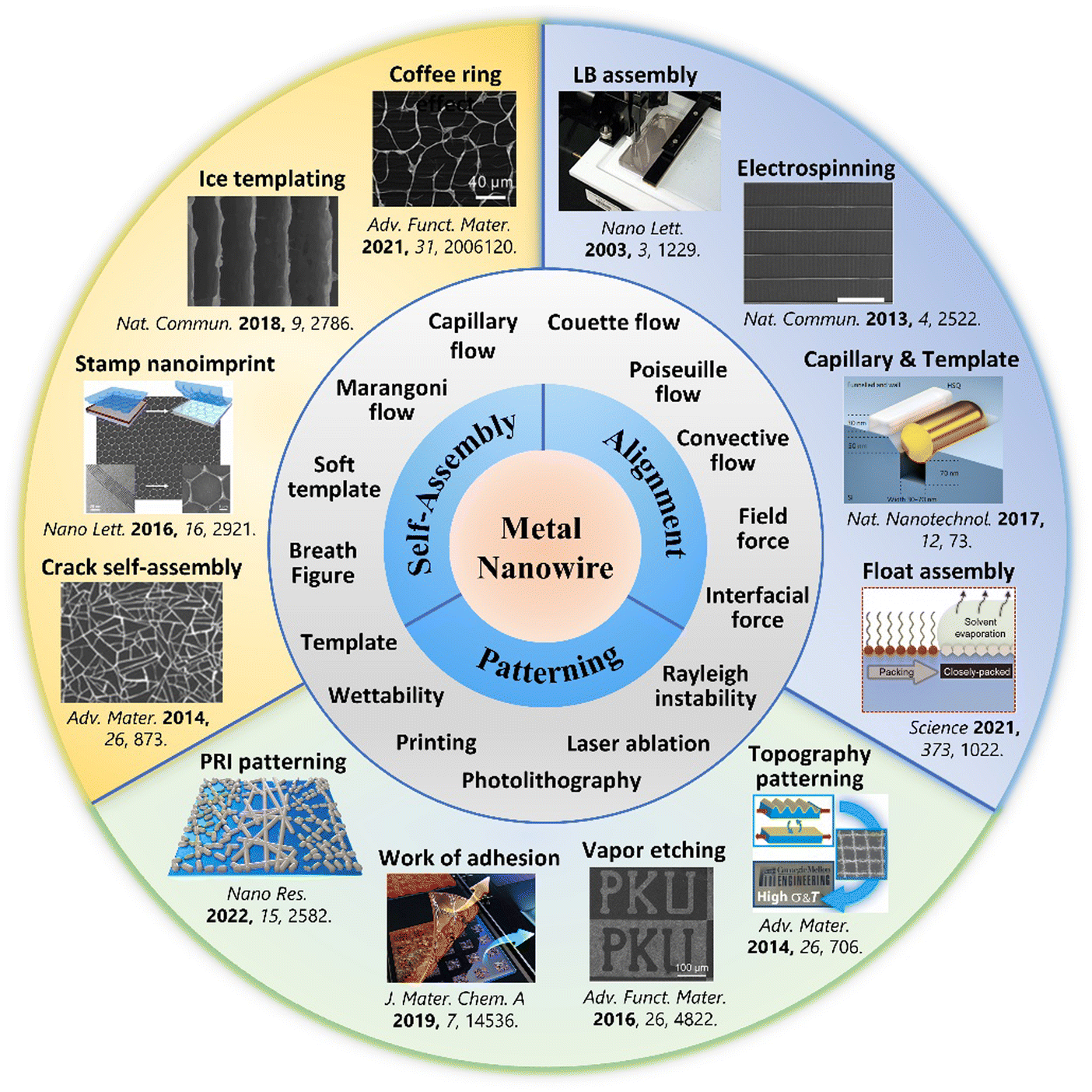 | ||
| Fig. 1 Summary of self-assembly, alignment, and patterning techniques of MNWs, along with involved fluid processes and parameters. Reproduced with permission.45,86,87,102–110 Copyright 2013, Springer Nature; Copyright 2015, American Chemical Society; Copyright 2017, Springer Nature; Copyright 2021, American Association for the Advancement of Science; Copyright 2014, Wiley-VCH; Copyright 2016, Wiley-VCH; Copyright 2019, The Royal Society of Chemistry; Copyright 2019, Springer Nature; Copyright 2014, Wiley-VCH; Copyright 2016, American Chemical Society; Copyright 2018, Springer Nature; Copyright 2022, Wiley-VCH. | ||
2. Self-assembly
Self-assembly of liquid-dispersed nanomaterials refers to the process in which nanomaterials spontaneously organize into an ordered, macroscopic structure through a specific liquid thermodynamic process. The structure is guided by a reduction in the system's interfacial/surface energy and/or external actions, mainly including the coffee-ring effect, liquid interfacial force (e.g., bubbles),47 direct interactions between the nanomaterials, external field (e.g., electric field),70 and templates (e.g., modified anisotropic substrates).111,112 The first four strategies are the “extra” template-free assembly methods. In the methods based on the coffee-ring effect and liquid interfacial force, the droplets or liquid–substrate interfaces are generally used as “soft” templates, at the edges of which the MNWs self-assemble after the liquid evaporation.34,45,47–51,113 The direct interaction method enables the assembly of MNWs into an ordered fiber or pattern but suffers from poor controllability.32,35,46 The above strategies can yield both specific patterns (nanorings, porous structures, microcircuits, etc.) and aligned structures of MNWs. For example, the self-assembly methods based on the coffee-ring effect,114 templates,36,114 and external fields87 are also applicable to the alignment and patterning of MNWs. Due to the numerous studies on the two topics, the self-assembly of MNWs into aligned and orderly patterned structures is described under the Alignment and Patterning sections, respectively.2.1. Coffee-ring effect-based assembly
The coffee-ring effect refers to the phenomenon in which ring-like patterns are left on a solid substrate after the evaporation of sessile droplets containing non-volatile solutes.115 The mechanism involved is that the evaporation rate at the inner edge of the droplet is greater than the evaporation rate at the center, which induces an outward capillary flow to carry suspended solutes to the edge of the droplet and form a ring-like deposition.116 This effect has been widely exploited for deposition of nanoparticles, polymers, and biomolecules,117 and recently extended to the assembly of MNWs into micromesh-like structures on macroscopic substrates, which mainly serve as high-performance conductors with large optical aperture ratio, high conductivity, and/or large stretchability.34,45,49The deposition pattern of MNWs is closely associated with the capillary flow and Marangoni flow, and their relative strength (Fig. 2a). The two flow processes can be effectively modulated by droplet size and the properties of ink and substrate.45 Using an atomization method to control the droplet size, Seong et al. achieved three kinds of ring-shaped AgNW structures (Fig. 2e).50 For large droplets with low evaporation rates, the AgNWs tend to be deposited along the circumference of the droplets via the capillary effect, yielding an AgNW ring with a thick rim and sparse deposition within the ring (the far left of Fig. 2e). With the decrease in droplet size and thus increased evaporation rate, the NW deposition is no longer dominated by the capillary flow and forms the coiling of AgNWs inside the small droplets. When the droplet diameter drops below a specific size, the deformed AgNWs form a nearly perfect ring. If a polymer material is dissolved in the solvent, a polymer-filled AgNW ring can also be achieved (Fig. 2d). As indicated in Fig. 2c, the final morphologies generated by the small droplets are guided by the relative values of the restoring force (FR) of the NW, arising from the NW length larger than the droplet size, and the compressive force (FC), a net force from liquid surface tension exerted on the NW surface.118,119 A stronger compressive force (FC > FR) can strongly bend the NWs to form a ring shape; the converse leads to randomly kinked NWs inside the droplet.
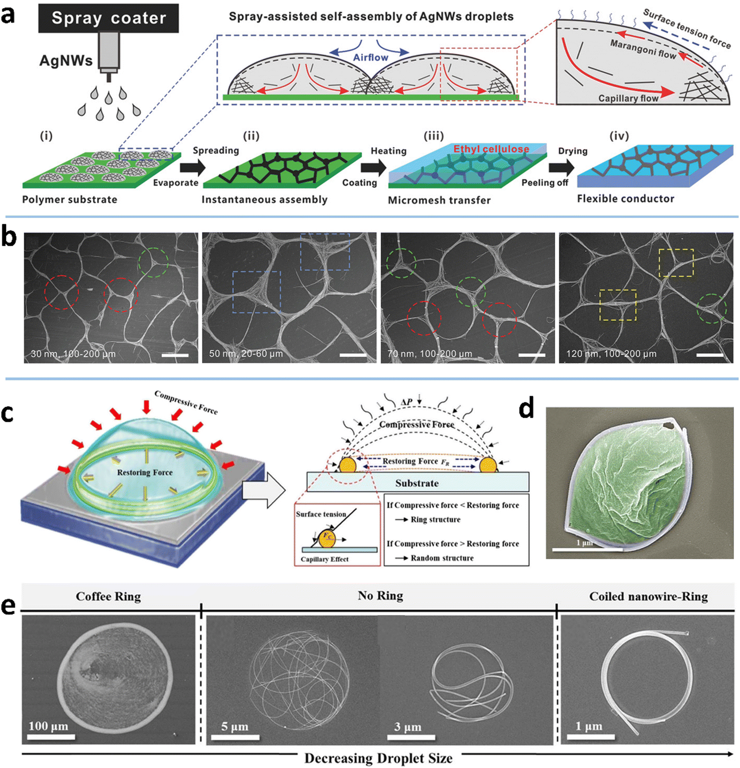 | ||
| Fig. 2 (a) Fabrication procedure and assembly mechanism of the AgNW micromesh. Reproduced with permission.34 Copyright 2018, WILEY-VCH. (b) Scanning electron microscope (SEM) image of the obtained AgNW microgrid. Reproduced with permission.45 Copyright 2021, WILEY-VCH. (c) Formation mechanism of the AgNW ring. (d) SEM image of the AgNW ring filled with polyvinylpyrrolidone (PVP). (e) SEM image of kinked AgNWs with different wetted droplet sizes. Reproduced with permission.50 Copyright 2017, American Chemical Society. | ||
High wettability of the NW ink on the substrate can induce a quick-spreading flow and rapid evaporation to produce uniform deposition within the droplet.114 Xiong et al. demonstrated that a hydrophobic substrate (perfluoroalkoxylalkane, PFA, with a water contact angle of 108.2°) facilitates the pinned droplets to expedite the capillary flow and suppress the Marangoni flow, giving rise to a microgrid structure through a spray-assisted process (Fig. 2a and b).34,45 Comparative experiments suggest that the substrates with surface tension higher than 25 mN m−1 are not suitable to form AgNW-bundle meshes for the IPA ink with AgNWs of diameter >20 nm due to the limited driving force within the spreading droplets on the substrates. As for the ink, a higher surface tension (by adding water into the IPA ink) has a larger contact angle and thus a smaller contact area, making the droplets slip freely during the slow evaporation of water. The coffee-ring effect is therefore weakened to form a uniform deposition of AgNWs.
MNW dimension also has a marked impact on the self-assembled morphology. It is easier to drive nanoparticles than the heavier MNWs under the capillary flow.120 The drop-casting of ethanol-dispersed AgNWs (diameter 200 nm and length 30 μm) on silicon yields relatively uniform deposition with a slightly thick rim.114 With a smaller size (e.g., diameter 40 nm and length 25 μm), most AgNWs can be transported to the rim by the capillary flow, yielding a ring-like deposition and micro-meshed structure.50 The shorter AgNWs form a mesh with larger bundles and knots (Fig. 2b), because the same weight ratio per unit area has a higher amount of the shorter NWs than the longer NWs.45 The resultant micromesh has a lower performance in terms of both conductivity and transparency. At a given length, the AgNWs with small diameters self-organize into a mesh with smoother knots, better connection, and thinner bundles due to the lower amount and better ductility of the thinner NWs, which results in higher conductivity and transmittance. It is also demonstrated that the AgNWs with higher aspect ratios form a mesh with larger cells and thicker bundles at high concentrations (≥2 wt%), while the results are mixed at low concentrations.49 One of the resultant TEs has a sheet resistance (RS = RW/L, where R, W, and L are resistance, width, and length, respectively) of 25 Ohm sq−1, an ultrahigh transmittance (T) of 97%, and a low haze (deviation degree of transmitted light) of 2.6%.34
To sum up, the assembly texture via the coffee-ring effect can be easily tuned and optimized by adjusting the properties of the solvent (including surface tension, volatilization rate, viscosity, etc.), MNW dimension, concentration and composition of the ink, surface energy of substrates, and the deposition method (spray coating, rod-coating followed by heating, etc.). Modulation of the coffee-ring effect can be achieved by controlling (i) the pinning of the contact line, (ii) the outward capillary flow, (iii) the Marangoni reflux, and (iv) the interaction between the liquid interface and NWs. The most prominent feature of this effect is the template-free assembly into specific patterns. Using a multi-nozzle spraying system, one could easily scale up the ring formation through the coffee-ring effect for mass manufacture of MNW-based TEs.
2.2. Ice template assembly
Interfaces are the most important assembly platform for the MNWs dispersed in solvents. With the use of different types of interfaces, such as the liquid–liquid interface and the solid–liquid interface, various strategies including freeze casting,36,121,122 breath figure (BF) method,51,123 bubble templates,47,48 LB assembly,56 crack-direct assembly,111,112etc. have been developed for self-assembly of NWs into 1D, 2D, and 3D structures. These strategies can realize either aligned NWs or NWs organized into microporous structures. The alignment of NWs will be discussed in a separate section, considering the numerous publications on this topic.Ice templating is a versatile solid–liquid interface-based technique for assembling various materials into porous structures.121 It is not until the 2010s that the ice templating gained much attention in MNW assembly.109,124–130 Typically, ice templating involves the controlled freezing of a liquid or liquid hybrid, freeze drying of the solvent (mostly water), and subsequent posttreatment (e.g., thermal annealing) if necessary.121 During the freezing process, the solvent solidifies into patterns that serve as a template, where the solidification front repulses solid nanomaterials to follow the template. Afterward, the ice template is removed by sublimation, leaving the nanomaterial-formed framework.
The most common type of structure assembled by the ice template technique is the 3D cellular-like hierarchical architecture (Fig. 3a), i.e., AgNW-based aerogel.109,124,125 The 3D cells are induced by the parallel ice fingers which are formed during ice crystals sweeping along with the solidification front. The AgNWs are rejected and condensed into the spaces between the ice fingers. In this way, the 2D AgNW networks with interconnected 3D cells are assembled into a macroscopic monolith. This MNW-based porous structure offers a new way to achieve ultrahigh ratios of conductivity to weight, e.g., a conductivity of 1.3 S cm−1 at a density of 1.3 mg cm−3,125 with tunable electromechanical stability. By combining the 3D MNW framework with hydrogels or elastomers one can construct high-performance stretchable and piezoresistive conductors. Yu et al. presented a first example of the combination of the sulfhydryl compound-modified 3D AgNW aerogel and a hydrogel (poly(N-isopropylacrylamide)) as the stretchable conductor,109 which has a cellular architecture with a ternary structure: NW network, cellular microstructure, and macroscopic assembly with hydrogel cross-linking. Unlike the elastomer-filled NW framework, the hydrogel-conjugated cellular-like AgNW structure effectively dissipates the crack energy to withstand a tensile strain of 800% with a minor change in resistance.
 | ||
| Fig. 3 (a) Illustration of the structure of 3D ice-templating AgNWs and the corresponding SEM image. Reproduced with permission.109 Copyright 2018, Springer Nature. (b) Schematic of the 2D recrystallized ice template method and the optical microscope (OM) image of the assembled 2D AgNW mesh. Reproduced with permission.131 Copyright 2017, American Chemical Society. (c) Schematic of the 2D ice-templating method for ordering and patterning AgNWs and the corresponding SEM image. (d) Schematic and SEM images of ‘>’ shaped and orthogonally aligned AgNW patterns fabricated by the 2D ice-templating approach. Reproduced with permission.36 Copyright 2021, WILEY-VCH. | ||
The ice template technique has also been extended to the 2D assembly of MNWs into a porous and ordered network. One strategy is the direct transformation of the 3D cellular structure into a 2D porous network during the ice thawing by the use of the high flexibility of ultrathin MNWs and the NW capillary coalescence.127 The other is the utilization of the salt-controlled recrystallized ice crystals as the 2D template for MNW assembly (Fig. 3b).131 The ice crystals at −80 °C were subjected to annealing at a higher temperature to trigger the recrystallization, leading to the growth of the crystals. The crystal size can be easily tuned by adding different ions and changing the annealing temperature. In this way, the mesh size and bundle width of the assembled 2D AgNW mesh can be regulated to achieve desirable optoelectrical performance and stretchability. Besides the porous network, an orderly patterned 2D network has been reported by directionally freezing a liquid film at a controlled velocity (Fig. 3c).36 By simultaneously freezing from two directional cold sources, ‘>’ shaped and orthogonally crossed patterns can be fabricated (Fig. 3d). The TE prepared from low-dose AgNWs exhibits an RS of 20 Ω sq−1 and a T of 91%.
2.3. Other types of interface assembly methods
The BF is another natural phenomenon which provides guidance for micro/nano fabrication. One example is the fog formed on a cold glass when we breathe upon it. The BF method can induce the formation of the honeycomb macroporous pattern (HMP) of MWNs with high transparency and conductivity.132 The typical BF method involves cast coating of a nonpolar, low-boiling point solvent, and harvest of water droplets on a substrate.123 The two-phase system serves as a soft template to induce a porous pattern of nanomaterials (Fig. 4a).133 He et al. used chloroform to disperse AuNWs and cast the dispersion on the Si substrate which was then placed in a closed humid container.51 As the solvent evaporates, small water droplets condense to form a droplet-array on the substrate.4 The AuNWs can self-assemble at the edge of the droplets to form the HMP when the water droplet-array evaporates completely (Fig. 4b). The concentration and length of AuNWs and the surrounding humidity are the critical parameters for the static BF method. For example, humidity affects the condensation of water, which in turn affects the size of water droplets and the shape of the hole-array. With a similar idea, Shin et al. achieved an AgNW microgrid on polyethylene terephthalate (PET) by rod-coating a formulation that consisted of AgNWs and three solvents (DI water, methanol, and α-terpineol).49 The three solvents constitute a multi-phase system to yield a soft template during evaporation. Since the vapor pressure of α-terpineol is 107 times higher than that of methanol, evaporation leaves two immiscible fluids: α-terpineol and water. The α-terpineol droplet separates the water containing AgNWs to form a cell-like separation texture with concentrated NW bundles after complete evaporation. The cell-shaped pattern not only improves the conductivity but also creates a high aperture ratio to have high transparency, showing an RS of 25.44 Ohm sq−1 at 88.42% transmittance and 3.71% haze. | ||
| Fig. 4 (a) Schematic illustration of the fabrication process for the porous HP-AgNW/TPU film. (b) Optical (i) and SEM (ii) images of the porous AgNW/TPU film. Reproduced with permission.133 Copyright 2020, American Chemical Society. (c) Schematic of ACNT-assisted self-assembled multidimensional structures of NWs. (d3–e3) Digital images of the assembled NW micro-structures. Reproduced with permission.35 Copyright 2019, WILEY-VCH. | ||
Likewise, other multi-phase induced interfaces have been developed to manufacture various metal grids with abundant open areas. Gong et al. reported a simple air–water interfacial self-assembly technique to fabricate a meshed TE using ultrathin AuNWs (diameter ≈ 2 nm).134 The aged AuNW hexane solution was drop-cast on the air–water interface. The immiscible hexane floated on the air–water interface and evaporated to assemble the AuNWs into a mesh-like network. Due to its ultrahigh aspect ratio (>10![[thin space (1/6-em)]](https://www.rsc.org/images/entities/char_2009.gif) 000) and small diameter, the network was comprised of serpentine bundles with an average thickness of 193.7 nm and pore sizes of 8–52 μm. The bundle formation may arise from the partial removal of oleylamine ligands from the AuNW surface. The AuNW network exhibits an RS of 130.1 Ohm sq−1 at 92% transmittance. Khatri et al. created the bubble-based air–liquid interfaces to guide the mesh formation of AgNWs.47 The AgNW water dispersion was bubbled using the surfactant sodium dodecyl sulfate and the thickening agent lauryl dimethylamine oxide. The bubbled solution was then cast and sandwiched between two substrates to form the meshed AgNW network after drying.
000) and small diameter, the network was comprised of serpentine bundles with an average thickness of 193.7 nm and pore sizes of 8–52 μm. The bundle formation may arise from the partial removal of oleylamine ligands from the AuNW surface. The AuNW network exhibits an RS of 130.1 Ohm sq−1 at 92% transmittance. Khatri et al. created the bubble-based air–liquid interfaces to guide the mesh formation of AgNWs.47 The AgNW water dispersion was bubbled using the surfactant sodium dodecyl sulfate and the thickening agent lauryl dimethylamine oxide. The bubbled solution was then cast and sandwiched between two substrates to form the meshed AgNW network after drying.
Using vertically aligned carbon nanotubes (ACNTs) on glass as a solid interface, Bian et al. assembled AgNWs into multidimensional ordered textures via fibrous elastocapillary coalescence (Fig. 4c).35 Due to its surface texture and inherent hydrophilicity, the ACNT can be gradually wetted by the AgNW water solution.135,136 Under the action of strong capillary force and van der Waals interaction, the ACNT fibers coalesce into a micropattern, on the top of which the AgNWs are densely arranged into the same pattern.137 Meanwhile, CNT filaments are drawn out and crossed over the mesh of the micropattern (Fig. 4c(d3–e3)). As a result, the multidimensional ordered AgNW/CNT hybrid micropatterns are formed, exhibiting a good piezoresistive effect with a sensitivity of 0.32 kPa−1.
3. Alignment
MNWs have distinct anisotropic physical properties which cannot be manifested and exploited in disordered structures. This section summarizes the methods to achieve macroscopic ordered in-plane MNW networks in which the long axes of individual MNWs are more or less parallel to each other (i.e., in alignment). The alignment strategies can be categorized into shear force-based approaches, LB technique and its variants, and electromagnetic field methods.3.1. Shear force-based alignment
In most cases, the system can be simplified as either the parallel-plate Couette flow or pipe Poiseuille flow. For the most frequently used IJP and rod/blade/slot-die coating, a meniscus connecting the substrate to the printing/coating head is also involved during the NW deposition. Therefore, the alignment of NWs is the synergistic action of shearing speed, solvent viscosity, height of the wetting film, solvent evaporation, NW aspect ratio, NW concentration, capillary action, and/or substrate properties. Fig. 5a illustrates the various flows and interactions affecting the NW alignments near the boundary. Without involving or before entering the meniscus, the alignment degree is mainly determined by the velocity field which has a linear profile for the Couette flow and a parabolic profile for the Poiseuille flow. In both cases, a higher shearing rate yields a higher degree of alignment for NWs.29,155 However, the orientation of a few NWs in the obtained samples deviates from the shear force direction because there is thermal relaxation before NWs adhere to the substrate. The relaxation can be evaluated by the Peclet number (Pe) and Reynolds number (Re). The Peclet number can describe the relative strength between hydrodynamic and diffusion forces of the NW in the liquid flow, given by156
Pe = 3![[small gamma, Greek, dot above]](https://www.rsc.org/images/entities/i_char_e0a2.gif) μl3/kBTln(R) μl3/kBTln(R) | (1) |
, μ, l, kB, T, and R are the shear rate, shear viscosity of the solution, length, Boltzmann constant, temperature, and aspect ratio of the NW, respectively. The NW motion is dominated by the flow field for Pe ≥ 1 but by the Brownian fluctuations for Pe < 1.156 The Reynolds number quantifies the influence of inertial forces compared to viscous forces, described by157| Re = ρvL/μ | (2) |
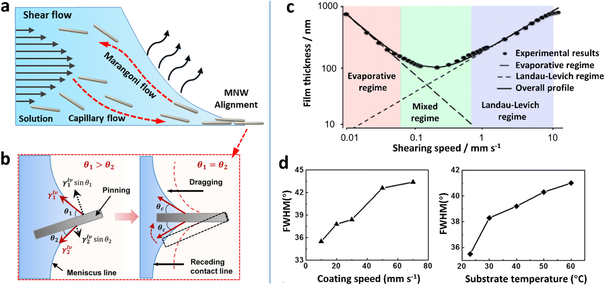 | ||
| Fig. 5 (a) Schematic of flows underlying the shear flow-guided coating that can influence the orientation of MNWs. (b) MNWs aligned by a nano-patterned PDMS stamp and the capillary action at the air–liquid–solid contact line. (c) Two deposition regimes as a function of coating speed. Reproduced with permission.157 Copyright 2018, Springer Nature. (d) FWHM values as a function of coating speed and substrate temperature. Reproduced with permission.91 Copyright 2017, American Chemical Society. | ||
The fluidic system is more complicated if a meniscus near the substrate is involved. Due to enhanced evaporation in the front of the meniscus, a capillary flow carrying NWs toward the contact line can be induced. In the meantime, a surface tension gradient along the meniscus may be generated depending on the solvent, which triggers a Marangoni flow to recirculate NWs back toward the deposition head (Fig. 5a). At the contact line, the pre-alignment NWs are subjected to unbalanced capillary forces to further improve the alignment degree (Fig. 5b). According to the flow speed, there are two deposition regimes: “evaporative regime” in which film thickness decreases with coating/printing speed and “Landau–Levich (LL) regime” in which film thickness increases (Fig. 5c).157 In the evaporative regime, low shear rates lead to the disordering of the MNWs through their rotation along Jeffery orbits under a small Reynolds number.158 A minimum coating speed of ≈1 mm s−1 is required for a shear force-based alignment of the AgNWs.91 Therefore, for highly aligning MNWs, the coating speed values reported in the literature are in the range of 0.5–100 mm s−1,86,91,94,96 which are located within the LL regime. With a LL meniscus, the thickness (h) of the liquid film can be given by the capillary number (Ca = μv/σ) as follows:157
| h = kCa3/2Rd | (3) |
Bubble blowing. Bubble blowing is one of the classic shear force-based methods for NW alignment.73,74,153,154 This method generally involves three steps: (1) preparation of polymer solution containing NWs; (2) expansion of the NW dispersion with a ring centered over the gas outlet, which was moved upward while introducing gas, and (3) transfer of the bubble film onto the target substrate. In this method, the NWs are oriented in the thin polymer film and at the interface between the film and the substrate, not in a fluid as in most shear-force based approaches. The MNW alignment is driven by the shear forces generated at the gas outlet and the interface upon attaching the receiving substrate, as well as by the tension force arising out of bubble blowing. Cao et al. used this method to align TeNW networks and in situ transformed the straight TeNWs into buckled nanosprings during the blowing process (Fig. 6g).73 This group also constructed sausage-like nanoblocks containing graphene nanotubes and CuNWs in the bubble film, which can enhance the antioxidation of Cu and reduce the linear resistance of graphene.159 Large-area crossed-aligned NW networks have been realized by the bubble-blowing method for application in gas sensors and FETs.160 This low-cost technique can print NWs on various substrates, whether their surfaces are flat, rigid, or not. However, two drawbacks remaining for this method are the control of density and distribution of MNWs on the substrate and the polymer matrix residing in the NW film which may decrease optoelectrical performance such as conductivity.
 | ||
| Fig. 6 Schematic illustrations of the (a) water-bath assisted convective assembly, (b) agitation-assisted alignment, (c) conical fiber array-guided alignment, and (d) capillary printing. (a–d) Reproduced with permission: ref. 28, Copyright 2015, The Royal Society of Chemistry; ref. 29, Copyright 2019, WILEY-VCH; ref. 161, Copyright 2018, WILEY-VCH; ref. 86, Copyright 2015, American Chemical Society. (e) OM images of the capillary-printed unidirectional AgNWs. Reproduced with permission.86 Copyright 2015, American Chemical Society. (f) SEM image of the convective flow-assembled bi-aligned AgNWs. Reproduced with permission.28 Copyright 2015, The Royal Society of Chemistry. (g) OM images of the crossed spring-shaped TeNWs. Reproduced with permission.73 Copyright 2014, American Chemical Society. | ||
Fluid convection. Fluid convection-induced shear force is a simple strategy for NW alignment. Heating and mechanical agitation have been used to induce the convection of MNW dispersion.28,29,162 A prestrained poly(ethyleneimine) (PEI)-coated polydimethylsiloxane (PDMS) film was placed on the wall of a beaker, in which the AgNW dispersion was magnetically agitated.29 The cationic polymer PEI was used to anchor aligned AgNWs in the agitated flow via electrostatic interaction. The alignment degree was improved by increasing solvent viscosity and agitation speed, but there existed an optimized viscosity for the highest orientation degree (Fig. 6b). The agitation at 800 rpm achieved around 50% of the NWs aligned within ±10°. By assembling AgNWs twice with orthogonal direction, a mesh-like AgNW network was achieved. The prestrain-induced tangled AgNW network shows a high stretchability of 40%, with a special positive relationship between the strain and conductivity. Heating the solvent in a beaker is another strategy to induce convection-based alignment.28,162 As shown in Fig. 6a, inhomogeneous heating causes an uprising stream and a down-flowing stream of water at the center and rim of the beaker, respectively.28 When a small droplet of NW solution (e.g., ethanol162 or IPA28 as the solvent) is drop-cast on hot water, the NW solution can quickly spread out on the water surface without NW precipitating or mutual dissolution, which may be caused by the interface heat convection arising from the temperature gradient between the mild droplet and hot water. The shear force induced by the Marangoni effect at the interface actuates the orientation of the AgNWs to form a shiny mirror-like layer when the solvent evaporates. The aligned AgNWs can be easily transferred to the target substrate by dip coating. Likewise, a crisscross NW mesh can be obtained by two-times dip coating (Fig. 6f). The major drawback of the bubble blowing and fluid convection-based methods is their impracticality in large-area fabrication.
Bar coating. Bar coating is a simple yet effective method to generate large-area aligned MNW networks.90–93,96 The bar here refers broadly to various sweeping heads including rod,94 Meyer rod,91,92,96 blade/plate,149 slot-die,163 structured bar,86 and even hairbrush.161,164 The NW alignment is not only induced by the shearing action underneath the bar, but is also affected by the downstream meniscus which involves capillary flow, Marangoni flow, and the capillary force at the contact line (Fig. 5a). In the LL coating regime, a higher coating speed (0.5–100 mm S−1) leads to a thicker meniscus and a lower alignment degree,94 indicating that the meniscus action dominates the NW alignment. It is reported that more than 85% of MNWs align within
±30° at a coating speed of 10cms−1.96
To further improve the alignment degree, efforts have been devoted to spatial heterogeneity of the bar and substrate. Takemoto et al. modified a substrate into a hydrophobic/hydrophilic patterned surface to provide additional boundary constraints for the glass-rod coating of AgNWs, reducing the RS by 6.8 times.90 Likewise, a structured coating head can provide physical guidance for MNW deposition. Our group first used the Meyer rod to achieve the aligned and bi-aligned AgNWs, which reduces the RS of the network by more than 50%, compared with the random AgNW network.92 Ko et al. modified the Meyer rod coating technique by preconjugating the PET substrate with poly-L-lysine to increase the AgNW adhesion to the PET via an electrostatic force.91 Similarly, mounting the coating bar with nano-patterned PDMS has been developed to more accurately guide the deposition of AgNWs. As shown in Fig. 6d, the PDMS with a line pattern spacing of 400 nm was attached to a trigonal prismatic frame, the sharp peak of which was in contact with the substrate, to sweep the AgNW solution on the substrate, producing a highly aligned or bi-aligned AgNW network (Fig. 6e). More recently, Liu et al. utilized the Chinese brush, composed of a conical fiber array (CFA), to achieve a highly oriented AgNW&PEDOT:PSS composite film (Fig. 6c). The conductivity of the CFA-aligned AgNW network along the brushing direction is over 270 times that of the spin-coated AgNW network. The advantages of the structured bar coating are that it provides additional geometric constraints which improve the alignment degree and evades the additional process requirements, such as transferring, substrate pre-patterning, and pre-grown vertical NW arrays, which are essential for other alignment approaches.4
Printing. Printing is another primary class of alignment technologies for MNWs, in which the gravure printing, IJP, and EHD jet printing have been reported to have alignment effects on AgNWs.165 The gravure printing shares a similar alignment mechanism with the blade coating for MNWs. The former differs from the latter in that the ink is coated onto engraved structures of a substrate and then transferred onto the target substrate. The gravure printing method has shown a full width at half-maximum (FWHM) value of 64.5° (smaller value indicating higher alignment degree), higher than the values of the capillary and Meyer-rod coating methods (Table 1). For the IJP and EHD jet printing (Fig. 7a), the shear force can be generated both on the surface of the jet stream and in the printed solution film. The two methods can precisely control the MNW deposition in terms of alignment, position, direction, and NW density. Different from the pressure-induced ink extrusion in IJP, the EHD jet printing utilizes an electric field to induce a conical ink meniscus at the nozzle tip so that the ink is ejected from the meniscus to form high-resolution patterns with printed features down to submicron size.166 The resultant MNWs are highly aligned without perceptible deviation, as shown in Fig. 7b.85 An additional benefit of the printing techniques is that the printed aligned MNWs can be easily constructed into a specific array or pattern with high resolution and performance,31,165 which will be described in Section 4.
| Nanowire | Method | Alignment degreea | Application | Ref. |
|---|---|---|---|---|
| a Alignment degree is characterized by FWHM. b ECG: electrocardiogram. | ||||
| AuNWs | Langmuir–Schaefer technique | ±10° | Chiral ultrathin films | 56 |
| AgNWs | Wetting–dewetting | 39.8° | Electrodes | 151 |
| AgNWs | Dip coating | 15°–75° | — | 88 |
| AgNWs | Dip coating | 17.3°–23° | Strain sensors | 167 |
| AgNWs | Bar coating | 35° | Flexible TEs | 90 |
| AgNWs | Bar coating | 21.4° | Flexible TPs | 91 |
| AgNWs | Bar coating | ±30° | Solar cells | 96 |
| AgNWs | Bar coating | 82° | TEs | 12 |
| AgNWs | Shear force | 57° | — | 168 |
| AgNWs | Shear force | ±30° | SEs | 29 |
| AgNWs | Gravure printing | 64.5° | — | 140 |
| AgNWs | EHD printing | ±10° | Heaters and ECGb sensing | 139 |
| AgNWs | Capillary printing | 40°–65° | LEDs and solar cells | 86 |
| AgNWs | Inkjet printing | ±30° | SEs | 82 |
| AgNWs | Grazing incidence spraying | ±15° | — | 169 |
| AgNWs | Substrate stretching | ±10° | — | 93 |
| TeNWs | Bubble blowing | <7° | Photodetectors and gas sensors | 73 |
| AuNWs | Printing and electric field | 22° | Muscle-tissue regeneration | 84 |
| CuNWs | Assembly by magnetic field | 8 ± 4° | — | 61 |
| FeNiCo NWs | Magnetic field and microgroove | 15 ± 1° | — | 62 |
| AuNWs | Assembly by electric field | 5° | — | 69 |
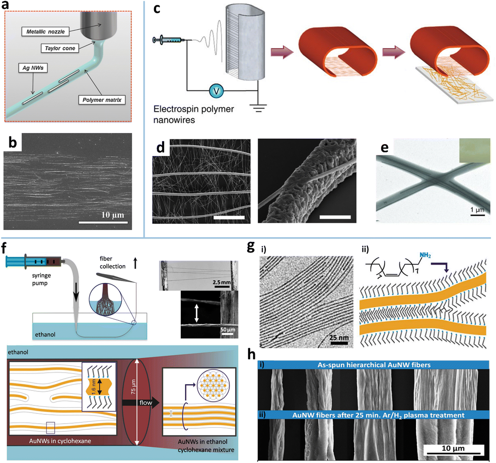 | ||
| Fig. 7 (a) Schematic of the EHD jet printing and (b) a corresponding SEM image of the aligned AgNWs. Reproduced with permission.85 Copyright 2014, WILEY-VCH. (c) Schematic of an electrospinning method for fabricating the aligned CuNWs–AgNW composite and (d) a corresponding SEM image of the aligned CuNWs integrated with random AgNWs. Reproduced with permission.102 Copyright 2013, Springer Nature. (e) TEM image of the electrospun fabricated PVP nanofibers containing aligned AgNWs. Reproduced with permission.75 Copyright 2012, WILEY-VCH. (f) Schematic of injection of AuNWs into ethanol and beam formation at the single NW level. (g) (i) TEM image of washed AuNWs and (ii) schematic illustration of two AuNWs with interacting ligand layers. (h) SEM images of AuNW fibers spun with different AuNW volume fractions before and after plasma treatment. Reproduced with permission.32 Copyright 2017, American Chemical Society. | ||
Pipe ejecting. Printing-like pipe ejecting techniques, electrospinning and solution spinning, have also been exploited to align AgNWs and AuNWs.75,76,80,81,170 The electrospinning technique was first developed to fabricate polymer fibers with diameters ranging from tens of nanometers to a few micrometers.102 As the electrostatic force generated by a high voltage overcomes the surface tension of the polymer droplet, a thin charged jet is formed and accelerated toward the grounded collector to produce ultrathin fibers (Fig. 7c). High alignment of the electrospun nanofibers can be easily realized by various auxiliary setups or external fields.171 The electrospun polymer nanofibers are used as either the matrix for containing MNWs or the template for further metallization to form MNWs. For the matrix strategy, MNWs can be aligned and incorporated into the nanofiber matrix by adding MNWs into the electrospinning solution.75Fig. 7e shows the aligned AgNW incorporated into PVP nanofibers. The AgNWs with a high aspect ratio show a higher alignment degree than the Au nanorods with a small aspect ratio.172
In the nanofiber-templated scheme, the key is to metalize the nanofibers to form MNWs. There are four main ways of metalizing nanofibers: calcination and reduction,77 thermal evaporation,102,173,174 electroplating,175,176 and electroless deposition.177,178 In the first method, the mixture of a metal precursor and a carrier polymer is electrospun to form raw nanofibers which are then subjected to calcination to obtain metal oxide nanofibers by removing the polymer, followed by reduction to turn the metal oxide into metal. The thermal evaporation is a more straightforward method, where the metal is thermally evaporated onto the electrospun polymer fibers to form metalized NWs after selectively dissolving the supporting polymer. Using this method, the Cui group fabricated a freestanding nanowire-like (nanotrough) network and a hybrid of aligned Cu mesowire (CuMW) and AgNWs via an additional transferring (Fig. 7c and d).102,173 It is shown that the aligned CuMW can decrease the RS of the NW TE by an order of magnitude without degrading T, showing RS = 0.36 Ω sq−1 at T = 92%. To avoid the high-temperature annealing or high-vacuum process, An et al. combined electrospinning and electroplating to produce a self-welded CuNW network.179 This method involves five steps: (i) noble-metal seeding on polymer fibers via vacuum sputtering or electroless non-vacuum chemical bath deposition to achieve sufficient electrical conductivity; (ii) electrospinning a supporting polymer fiber layer; (iii) electroplating in a copper electroplating solution for a few seconds; and (v) transferring the CuNWs onto target substrates and removing the supporting layer. To further simplify the process, Yang et al. proposed an electroless deposition of Cu on electrospun poly(4-vinylpyridine) (P4VP) NWs.179 The P4VP NWs as templates can be seeded with catalyst Pd nanoparticles in PdCl2/HCl solution due to the strong affinity of pyridyl groups to metal ions. The Pd NPs as catalysts induce reduction of Cu precursors onto the PVP NWs. The advantages of the electrospinning method are that high alignment of MNWs can be achieved at a macroscopic scale and more complex hierarchical alignment structures can be readily realized by controlling the arrangement of the electrospun fibers. It should be noted that the MNWs made by calcination, electroplating, and electroless deposition have rough surfaces, leading to lower conductivity. The performances of the resultant TEs are lower than those of MNWs fabricated by vacuum thermal deposition.
Solution spinning. Alignment of MNWs can also be achieved by solution spinning that utilizes intermolecular non-covalent interactions between MNWs to induce their self-assembly into freestanding fibers.32 In a study reported by Beate et al., the AuNWs in the cyclohexane dispersion are injected into the antisolvent ethanol to form fiber-like precipitates (Fig. 7f). When pulled across the ethanol–air interface, the fibers composed of loose AuNWs will be compressed by capillary forces. The ethanol induces fully interdigitated ligand layers (oleylamine) between adjacent AuNWs to yield tight bundling (Fig. 7g and h (i)). The bundles can be fully annealed by plasma treatment, forming porous NWs with continuous gold shells (Fig. 7h (ii)). The breaking stress of the well-aligned bundle is 25% higher than that of the poorly aligned bundle. The bundle fibers can be used to construct small electronic circuits or to form nanoscale interconnections.108
3.2. Langmuir–Blodgett technique and its variants
The LB assembly technique is one of the most classic methods for aligning nanomaterials, including NWs,53,87,100,180 NPs,181,182 nanotubes,55,183 and nano-films.30,52,54,184 A macroscopic LB assembly-like phenomenon is the “logs-on-a-river”, where the narrow river width causes the woods to be aligned along the flow direction. This alignment mechanism also applies to 1D nanomaterials. Typically, the 1D NWs diffusing on the surface of organic solvents generate a randomly distributed and loosely stacked NW network (Fig. 8a).185 Using a baffle with controllable surface pressure and barrier velocity to compress the layer on the liquid surface, a high-density aligned Langmuir monolayer film can be obtained (Fig. 8b). The aligned single-layer films can be repeatedly deposited by vertical immersion or horizontal lifting techniques, which can prepare nano-films with specific thickness or multi-alignments. For example, Wang et al. reported a transparent electrochromic film based on an ordered NW network with tunable conductivity (7–40 Ω sq−1) and transmittance (58–86% at 550 nm), which was obtained by depositing two layers of aligned NWs with crossing angles.186 The film-forming process was carried out under normal temperature and pressure, and it did not change the properties of the material itself. So far, ordered NW films, such as AgNWs,54 vanadium dioxide NWs,187 and germanium NWs,188 have been prepared by LB technology. Although the LB technique has demonstrated its versatility for NW assembly, it also has several drawbacks: NWs have to be surface functionalized, the LB process is slow, and the condition control is rigid, otherwise, NW array films are not uniform.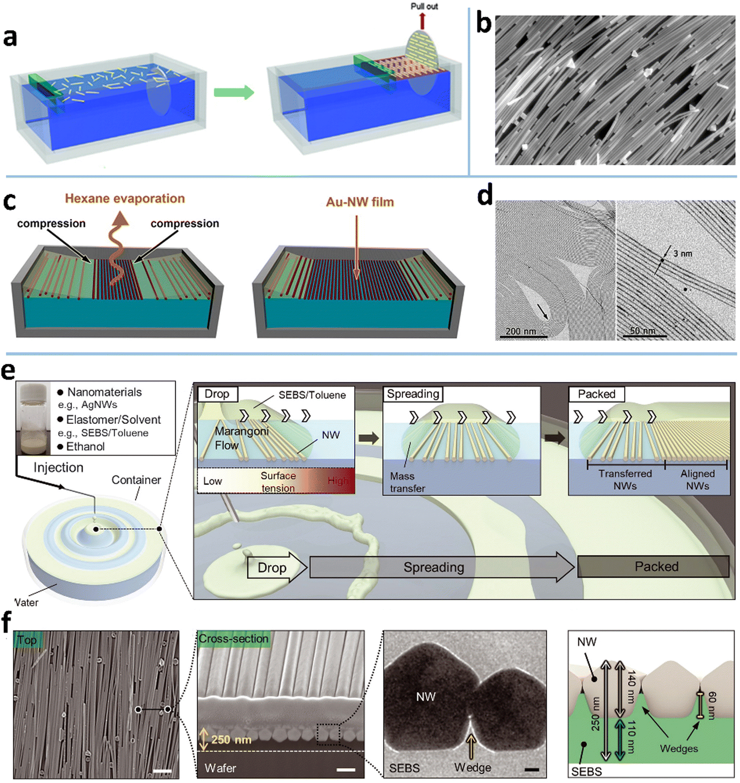 | ||
| Fig. 8 (a) Schematic of the LB assembly process. Reproduced with permission.100 Copyright 2012, American Chemical Society. (b) Aligned AgNWs achieved by the LB assembly method. Reproduced with permission.180 Copyright 2012, American Chemical Society. (c) Schematic of the convection-assisted technique for fabrication of AuNW monolayer films and (d) the TEM images of the assembled AuNWs. Reproduced with permission.53 Copyright 2012, American Chemical Society. (e) Schematic of a float assembly method for fabricating a compact, aligned AgNW nanomembrane. (f) SEM and TEM images, and structure diagram of the aligned AgNW nanomembrane. Reproduced with permission.87 Copyright 2021, American Association for the Advancement of Science. | ||
A few attempts have been made to overcome the above issues of the LB method. To avoid inhomogeneities that appear commonly in film transfer in the LB technology, Ana et al. reported a modified LB technique for AuNWs, which incorporates a meniscus-assisted float assembly on a liquid (Fig. 8c).53 A concave meniscus of hexane containing AuNWs is established on diethyleneglycol. The solvent evaporation rate is faster in the middle of the meniscus to induce NW compression at the liquid–air interface,189 which causes the AuNWs to be densely arranged with good alignment on a Teflon recipient (Fig. 8d).190 This process produces an almost defect-free dense NW monolayer with 2 nm thickness, showing a high T of 96.5% at a low RS (400–500 Ohm sq−1). Yang et al. developed a shear-assisted-Langmuir technique to align NWs.52 The NWs are first dispersed at the air–water interface in a funnel container and compressed by draining the water out of the funnel, accompanied by rotating the water by a polyrod to induce shear force that aligns the MNWs. Compared with the traditional LB technique, this method can produce aligned MNWs faster.
Recently, D. H. Kim et al. proposed an LB-like float assembly method to fabricate a dense aligned AgNW nanomembrane.87 Unlike the conventional LB technique, the NW compression in this method is induced by Marangoni flow at the water–oil interface, where the “oil” made of AgNWs, ethanol, and water-immiscible solvent elastomer floats on the water (Fig. 8e). The Marangoni flow is induced when the ethanol in the “oil” dissolves into the water to form a surface tension gradient. In the meantime, the water-immiscible elastomer solution floats on the water to create the oil–water interface, at which the AgNWs tend to settle due to the amphiphilic ligand (polyvinyl pyrrolidone). To further pack the AgNWs on the water, a few surfactant drops are dripped into the film center to induce Marangoni flow again. One advantage of this method over the LB assembly is that the aligned NW monolayer is partially embedded in an ultrathin elastomer film after the solvent in the “oil” evaporates (Fig. 8f). This film can be used as a skin electrode or transferred to target substrates for other uses.
3.3. Electromagnetic field methods
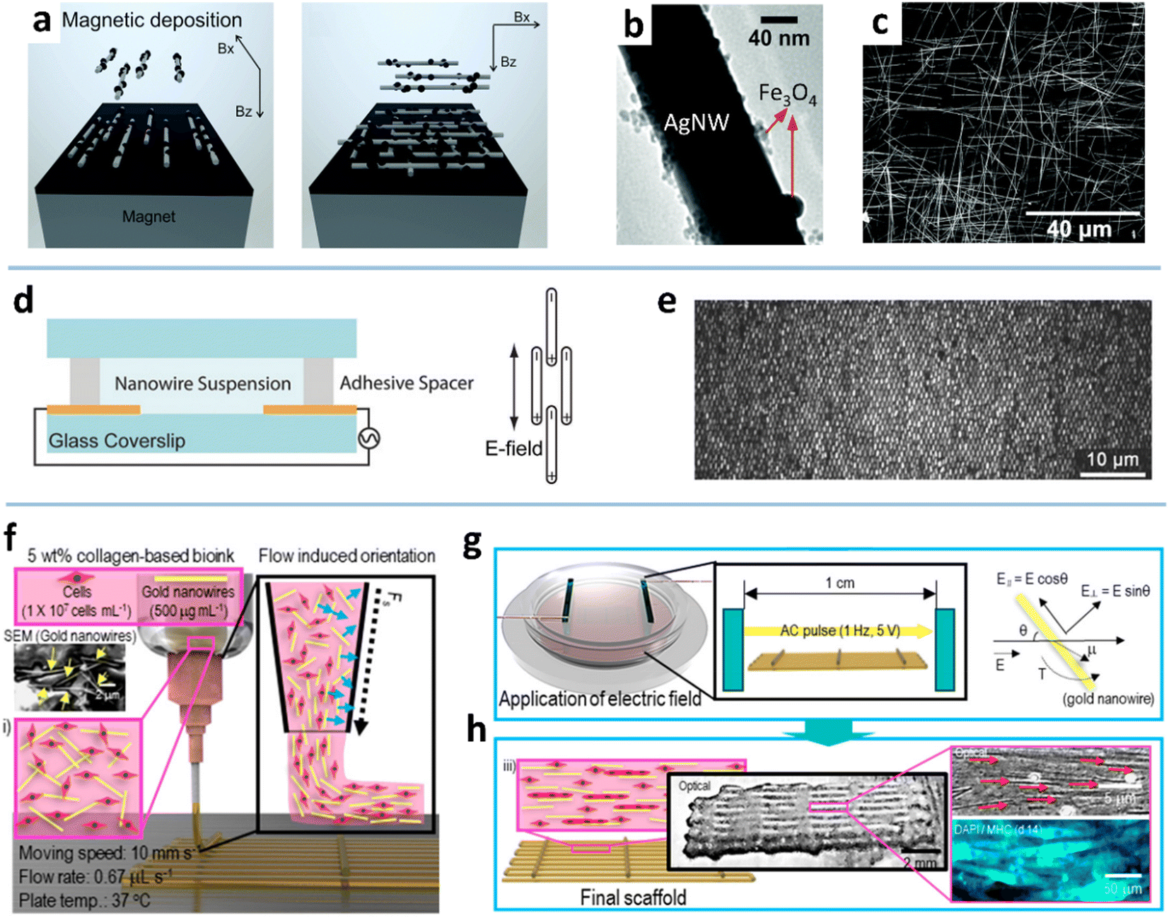 | ||
| Fig. 9 (a) Illustration of the alignment of Fe3O4–AgNWs in the magnetic field. (b) TEM image of the Fe3O4–AgNW. (c) SEM image of the bi-aligned Fe3O4–AgNWs. Reproduced with permission.63 Copyright 2015, RSC Pub. (d) Schematic of the electric field-induced assembly of AuNWs. (e) Reflected light OM image of AuNWs. Reproduced with permission.194 Copyright 2016, WILEY-VCH. (f) Schematic of the cell-printing process. (g) Schematic of the applied electric field for aligning AuNWs. (h) Schematic and optical/fluorescence images of the cell-laden collagen/aligned AuNW structure. Reproduced with permission.84 Copyright 2019, American Chemical Society. | ||
Two processes govern the ordered deposition of NWs in the magnetic field: NW rotation in suspension along the direction of the magnetic field line and NW approaching the substrate via NW–interface interaction. The rotation is closely related to the applied magnetic field strength, NW length, and solvent properties. Increasing the magnetic field strength has been shown to improve the alignment degree.62 At a given magnetic field strength, the shorter NWs can align better with the direction of the magnetic field before deposition on the substrate because the shorter NW has a higher velocity than a longer NW.62 The properties of the solvent, such as viscosity, also should have an impact on the NW alignment under a magnetic field, but there is still a lack of research on this topic. On the other hand, NW approaching the surface can be controlled by combining the magnetic field and heterogeneous substrates, as auxiliary templates, to improve the alignment degree. The geometrically structured substrate (e.g., micro-trench) can physically fix the NWs along the topography to reduce the MNW dislocation under a magnetic field.62 Even without a magnetic field, MNWs can be roughly aligned along the micro-grooves due to the capillary action of the radial outward flow and the high specific gravity of MNWs.104 The chemically patterned substrate can also increase the interaction between the MNWs and the substrate to form a better alignment.61,195 For instance, the carbon-doped silicon dioxide (CDO) substrate is selectively functionalized with thiol functional groups by photolithography,196,197 so that the Ni-modified CuNWs can be chemically anchored to the exposed thiol groups and selectively removed by a lift-off process. The prepared NW array exhibits high conductivity and good corrosion resistance because of the Ni shell.198
000 electrode sites covering 400 mm2.64 Also, crossed MNW networks can be obtained by layer-by-layer deposition with orthogonal electric fields. The MNWs aligned by dielectrophoresis have been used to fabricate various functional components, such as light-emitting diodes, resonators, and mechanical oscillators.65,94,201,202 Kim et al. gained the myoblast alignment with aligned AuNWs, which were achieved by a cell-printing process assisted with an electric field (Fig. 9f–h).84
The MNWs behave differently in a direct current (DC) and an alternating current (AC) electric field.69,203 In a DC electric field, according to qE = Kηv (where K is the drag coefficient, E is the electric field intensity, and η is the viscosity), the MNWs eventually move at a speed v, but the direction is random. The movement of MNWs in the AC field is determined by a dielectrophoretic (DEP) force: FDEP = 1/2εmRe(K)∇E2 (where εm is the dielectric constant of the medium, K is the Clausius–Mossotti coefficient). It is clear that the MNWs have no tendency to move in the AC electric field, but they will align in the same direction. Fan et al. used hybrid dielectrophoresis to align and transport MNWs based on this property.69 When a mixed DC and AC electric field is applied to the MNWs, they can control the NW direction while maintaining a linear trajectory. The DC and AC electric field intensity and direction angles can be appropriately adjusted by engineering electrode configuration.
On the whole, significant advances have been made in the development of alignment techniques, which are classified into three kinds: (1) shear flow-induced alignment; (2) LB approach and its variants; and (3) electromagnetic force-guided deposition. Advanced strategies have already reduced the alignment degree (characterized by FWHM) to ≤15°, roughly in the descending order LB technique > electromagnetic field method > shear flow approach (see Table 1). The shear flow approaches such as rod coating have excellent manufacturability at a compromised FWHM, whereas the LB techniques can yield a highly aligned, compact MNW film and the electric field-based methods enable precise assembly of MNWs between electrode couples.
4. Patterning
MNW networks need to be patterned to improve performance, realize new functions, or construct integrated devices. The reported patterning approaches for MNWs can be classified into top-down and bottom-up strategies. Top-down strategies are those in which uniform networks of MNWs are first deposited on substrates and then carved into specific patterns. Lithography,37,106,204–220 Plateau–Rayleigh instability (PRI) method,98,221–224 and laser ablation225–230 are the representative top-down techniques. In contrast, bottom-up strategies are those that directly organize MNWs into a particular structure on substrates, typically including printing,139,140,143,231–240 wetting–dewetting self-assembly,99,151,241–244 and template assisted patterning.4.1. Top-down strategy
Photoresist-based photolithography. Photolithography is the most widely used patterning technology which was initially developed for fabricating semiconductor integrated circuits in the 1960s. In early reports, photolithography is combined with electrodeposition to achieve patterned NWs of noble metals (gold, palladium, platinum, or bismuth).245,246 A temporary sacrificial template (nickel or silver) is fabricated by photolithography to act as a plating electrode which produces the patterned MNWs with 5–200 nm height and 0.011–2 μm width. More often, photolithography is used for patterning synthesized MNWs, which is elaborated in the following.
A key feature of photolithography is the pattern transfer from a photomask to a photoresist coating by light exposure. The method typically includes six steps: MNW deposition, liquid photoresist overcoating on the MNWs, pattern transfer, developing, selective removal of MNWs, and photoresist stripping (Fig. 10a and b).204,217 After developing the photoresist layer,211 structured access to the MNW network is produced to allow selective removal by wet/dry etching or exfoliation. Wet etching is the most commonly used, which employs liquid etchants to corrode MNWs. The etching effect can be improved either by adjusting the composition ratio and the pH value,209,247,248 or with external assistance such as sonication and oxygen plasma treatment, to shorten the processing time and achieve high-precision patterning.210,213 Dry etching mainly refers to processing MNWs using the physical and chemical processes generated by plasma discharge.249,250 There is also a report of using a neutral iodine vapor, as an etchant, to etch the exposed AgNWs, which achieves a pattern resolution of 5 μm with sharp edges.105
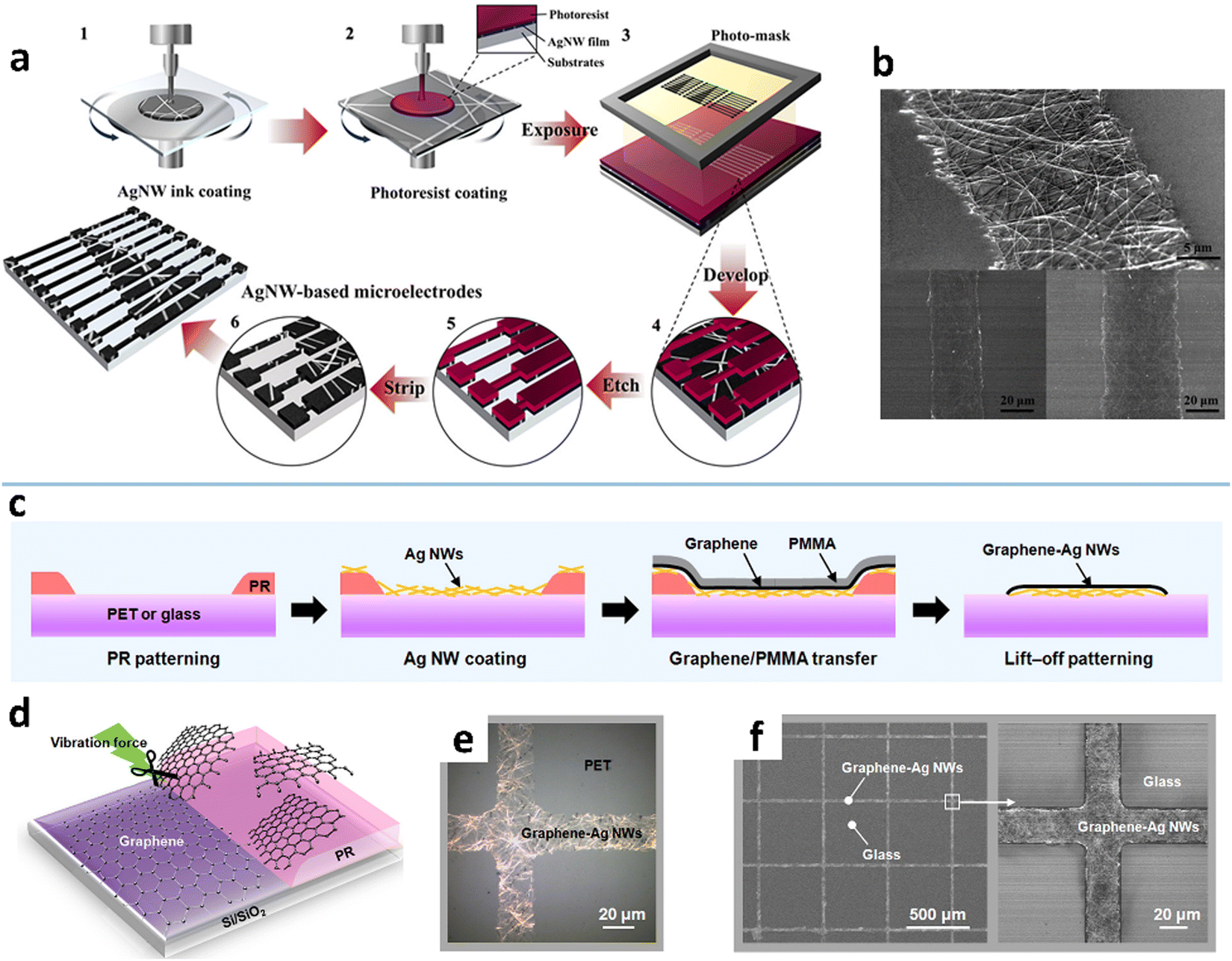 | ||
| Fig. 10 (a) Fabrication procedure of AgNW microelectrodes by a photoresist-based photolithographic process and (b) the fabricated AgNW patterns. Reproduced with permission.204 Copyright 2014, American Chemical Society. (c and d) Schematic of a lift-off photolithographic process for the graphene–AgNW composite. (e) OM and (f) SEM images of the graphene–AgNW patterns. Reproduced with permission.216 Copyright 2017, American Chemical Society. | ||
To avoid using environmentally hazardous or expensive etching processes, etching-free photolithographic methods have been developed for patterning MNWs. One is to use the dry film photoresist (DFR) to replace the liquid photoresist. The DFR can be directly laminated with MNW networks with no need for homogenization, baking, and curing. The MNWs underneath the UV-exposed DFR can be selectively removed by stripping the DFR or washed away by ethanol.212,251 The fabricated AgNW electrodes with a minimal linewidth of 50 μm show clear edges.212 The other is the lift-off technique which begins with photoresist patterning and then coating of the MNW film on the pattern, followed by selective removal of the MNWs through photoresist stripping (Fig. 10c and d).214–216 The graphene–AgNW composite is patterned into a minimum linewidth of 20 μm (Fig. 10e and f). Nevertheless, the above etching-free photolithography still requires the photoresist processes, including patterning, developing, and removing, which are complex, costly, and not environmentally friendly.
Photoresist and etching-free photolithography. This method modulates the adhesion of MNWs to the substrate to achieve patterning with external force such as physical exfoliation and ultrasonication.37,106,218,252 According to the adhesion theory, adhesion arises from mechanical interlocking, physical adsorption, chemical bonding, diffusion, and electrostatic charges.106 Physical adsorption, mechanical interlocking, and chemical bonding are the most frequently used to increase the adhesion between AgNWs and substrates.253–256 Considering a sandwich structure comprised of a UV-curable polymer, a AgNW network, and a substrate, the transfer of the AgNW network onto the target substrate is dependent on the difference between the mechanical interlocking strength (Wpoly-AgNW) and the physical adsorption strength (WAgNW-substrate) (Fig. 11a). The physical adsorption strength between two films is characterized by the work of adhesion (W1,2)106
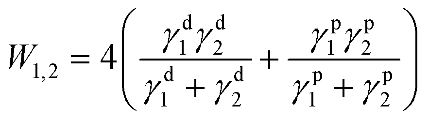 | (4) |
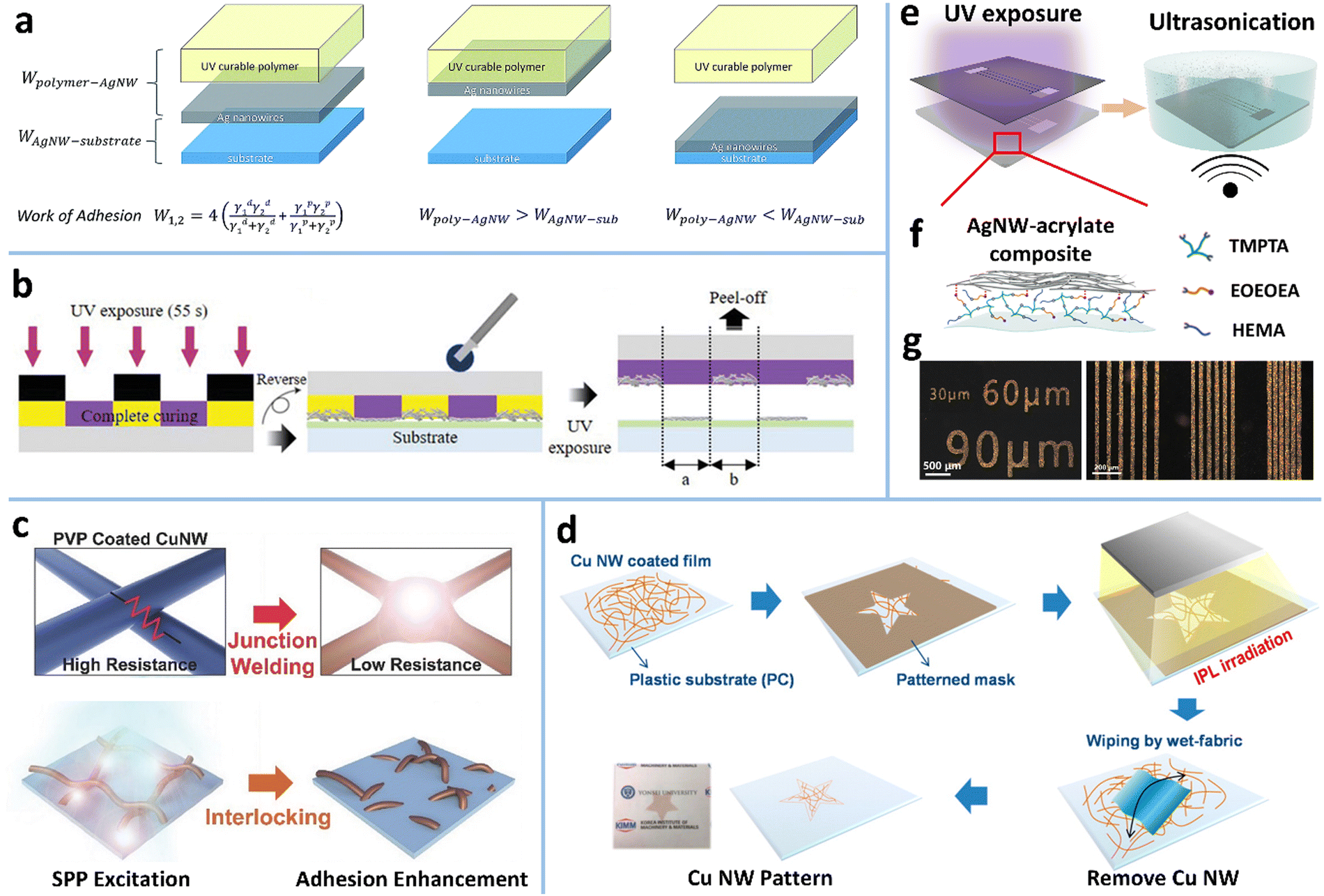 | ||
| Fig. 11 (a) AgNW patterning based on the difference in work of adhesion between AgNWs and two different substrates. Reproduced with permission.106 Copyright 2019, Royal Society of Chemistry. (b) Schematic of the UV-curable adhesive film-based photolithographic method for AgNWs. Reproduced with permission.257 Copyright 2021, WILEY-VCH. (c) Schematic of the IPL-induced nano-welding and interlocking of CuNWs. Reproduced with permission.258 Copyright 2017, WILEY-VCH. (d) IPL-based patterning process of CuNW electrodes. Reproduced with permission.220 Copyright 2016, American Chemical Society. (e) One-step photolithographic patterning method of AgNWs based on (f) a photosensitive AgNW-acrylate composite ink. (g) OM images and photograph of the AgNW patterns on PDMS with different sizes and line spacing. Reproduced with permission.37 Copyright 2020, American Chemical Society. | ||
Intense pulsed light (IPL) has also been utilized to realize the mechanical locking-based patterning of MNWs (Fig. 11c and d). The surface plasmon polariton (SPP) of MNWs can be excited by IPL to generate high local heat. The underlying polymer substrate is partially melted to make the MNWs embedded in the substrate, thereby enhancing the adhesion due to mechanical locking (Fig. 11c).258–261 Meanwhile, the strong electromagnetic coupling at the junctions of MNWs is triggered under the IPL to induce plasmonic nano-welding of MNWs, which significantly improves the conductivity of the MNW network. Selective adhesion of the MNW network is obtained by IPL exposure through a photomask. The unexposed MNWs can be easily recycled or removed by swabbing, taping, or ultrasonic cleaning.219,220,262 Combined with a roll-to-roll (R2R) system, this method can produce patterned flexible MNW TEs continuously.220 The prerequisite for this method is that the substrate must be a thermoplastic material, such as colorless-polyimide (cPI), PET, polyethylene naphthalate (PEN), and thermoplastic polyurethane (TPU), to ensure that it can be melted by SPP-induced heat.219,252,263 It should be noted that excessive high irradiation energy would cause the breakdown of MNWs and thermal deformation of the polymer substrate.
Chemical bonding-modulated adhesion based on photosensitive inks has also been exploited to achieve MNW patterning. Our group developed a photosensitive AgNW ink that functions as both a photoresist and an adhesion promoter to achieve etching-free one-step photolithographic patterning of AgNWs (Fig. 11e).37 The ink is comprised of AgNWs, ethanol, acrylate monomers, and a photoinitiator (Fig. 11f). The coated AgNW–acrylate composite film was selectively irradiated by UV light. The exposed film was polymerized and had strong adhesion to the hydroxylated PDMS surface due to the hydrogen bonding effect, while the unexposed film was water-soluble and could be removed by ultrasonication in water. This process yields well-defined AgNW micropatterns with a line width of 30 μm and a line spacing of 10 μm (Fig. 11g).37 Similarly, photosensitive N-methyl-4(4′-formylstyryl) pyridinium methosulfate acetal (sbq-PVA) and PEI were also used to prepare a photosensitive AgNW ink.264 The difference from the above method is that the AgNWs in the UV-irradiated region are buried and insulative in the cured polymer, while the AgNWs in the shadowed region are retained through the adsorption of PEI and exposed after rinsing sbq-PVA with water. The resultant pattern shows tiny optical visibility.
The most common strategy is to insert an adhesion promoter between MNW films and substrates. Poly(methyl methacrylate) (PMMA) templates as the mechanical locking layers have been printed on AgNW networks by IJP to achieve MNW patterning (Fig. 12a).218 The uncovered AgNWs can be selectively removed from the substrate by wiping with wet tissue or peeling off with tape, giving rise to patterns with a linewidth of 60 μm. If polyvinyl alcohol (PVA) film was coated on the PMMA-patterned AgNWs and peeled off, the positive and negative AgNW patterns with minimal size down to 10 μm are simultaneously achieved.238 The disadvantage of this method is the additional requirement of removing the PMMA template. To avoid dissolution of the chemical, the toner containing a polymer binder was printed into an image on a copy paper, which was used to transfer the AgNWs on a hydrophobic film by a hot-press process (Fig. 12b and c).237 The transferred AgNWs without the toner are weakly bonded with the paper and can be easily removed by taping, swabbing, or stamping with a polymer, while those embedded in the toner are retained, giving rise to a patterned electrode. Similarly, a fused deposition modeling (FDM) process using a 3D printer was used to define and transfer a kirigami pattern of AgNWs with no need for a hydrophobic donor substrate (Fig. 12d),266 on which AgNWs are not easily deposited uniformly by the solution process. The AgNW pattern is determined by and embedded in the first layer of TPU. The 2nd–5th layers define the overall shape and a 3D notch that guides the folding of the kirigami pattern. The kirigami/origami-structured electrode could construct a perovskite solar module with a stretchability of up to 400%. In another report, poly(3,4-ethylenedioxythiophene):poly(styrenesulfonate) (PEDOT:PSS) was employed as the transfer template for AgNWs.235 With a hot pressing process, the adhesion of AgNWs to PDMS is reduced, and the melting of D-sorbitol in PEDOT:PSS makes the AgNWs embedded in PEDOT:PSS, which allows for selective transfer of AgNWs. The conductive PEDOT:PSS can not only provide electrical contacts between AgNWs, but also increase adhesion and reduce roughness of AgNW electrodes.
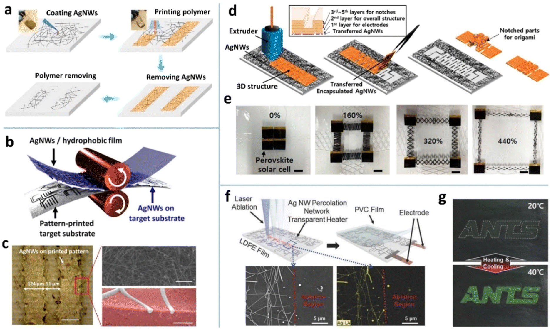 | ||
| Fig. 12 (a) Patterning process of AgNWs with a printed PMMA template. Reproduced with permission.218 Copyright 2019, Springer Nature. (b) Schematic of a toner-based transfer process for AgNWs. (c) A dry-transferred AgNW pattern and the corresponding SEM image. Reproduced with permission.237 Copyright 2017, American Chemical Society. (d) Schematic of a 3D printer-based AgNW patterning method for constructing kirigami/origami electrodes. (e) The fabricated system fixed on a stretchable elastomer for a sufficient restoring force. Scale bars, 2 cm. Reproduced with permission.266 Copyright 2019, American Chemical Society. (f) Schematic of laser patterning of AgNWs on a low density poly ethylene (LDPE) film for constructing a soft actuator. SEM and EDS images of the patterned AgNW network. (g) Color changes of the thermochromic ink layer. Reproduced with permission.267 Copyright 2018, WILEY-VCH. | ||
As an accurate, non-contact, mask-free tool, laser direct writing has been widely reported to achieve MNW patterns (Fig. 12f).225,226,228,230,267,269 The disadvantage of this method is the damage to the substrate which exhibits distinct ablation traces. Fortunately, a nano/femtosecond laser can directly transform the MNWs into a plasma state without any thermal melting process, yielding well-defined patterns without damaging the substrate.225,229,230 Fang et al. obtained an AgNW pattern with a linewidth as low as 20 μm by laser ablation and applied it as the bottom TE of a quantum dot light emitting diode (LED).227 Tran et al. optimized the parameters of nanosecond pulsed laser ablation for patterning ultra-long CuNWs and reported the optimum conditions: 10 mJ cm−2 fluence, 40 kHz repetition rate, and 0.5 m s−1 scanning speed.230 Liang et al. evaluated the ablation threshold of AgNWs and PET to realize high-precision patterning of AgNWs on a PET substrate by controlling the energy of femtosecond laser irradiation.229 In short, laser ablation is a facile, mask-free patterning technique that is suitable for MNW networks of different shapes and sizes; however, it has the demerits of low productivity and high cost in equipment.
Selectively triggering PRI is the key to achieving patterned MNW networks, which can be realized via three strategies. The first strategy is the use of a pulsed laser with a small spot to trigger the PRI of MNW networks selectively.221,222,224,271 Selectively coating the MNW network with thermally stable materials is the second strategy to control the PRI process.272–275 Indium zinc oxide (IZO) was coated on AgNWs and then irradiated by deep ultraviolet (DUV) that induces the M–O–M condensation reaction of IZO.223 The IZO capping greatly improves the thermal stability of AgNWs, while the non-irradiated IZO is removed to trigger the PRI of AgNWs at 250 °C, forming AgNW patterns with a resolution of about 100 μm. However, this method requires a relatively high heating temperature, which is unsuitable for flexible substrates.
To lower the triggering temperature of PRI, our group proposed two surface modification methods for AgNWs.98,110,276 One is the modification with diphenyliodonium nitrate (DPIN), which can be self-assembled into nanoparticles on AgNWs after spin coating (Fig. 13a and b).98 The DPIN NPs expedite the surface atom diffusion due to the gradient of chemical potential near the NPs (Fig. 13d). Furthermore, DPIN modification can form a thin cladding of a molten salt-like compound on the AgNWs at an elevated temperature. The two effects decrease the degradation temperature (Td) of the AgNW network by around 80 °C. Because of the hydroxy propyl methyl cellulose (HPMC)-enhanced plasmonic effect and the photo decomposable property of DPIN, nanowelding of AgNWs and pattern transfer can be simultaneously achieved by one-shot UV irradiation through a photomask (Fig. 13c). Then, low-temperature annealing (145 °C) can yield an AgNW pattern with a minimal size of 3 μm, which is the highest patterning resolution ever reported on AgNW microelectrodes. Moreover, the PRI-fragmented AgNWs in the unexposed region can be further removed by ultrasonication in water (Fig. 13e). The other is the modification with sulfhydryl compounds which form self-assembled monolayers (SAMs) on AgNWs via the Ag–S covalent bond (Fig. 13f).276 It is found that the alkanethiol SAMs activate the PRI of AgNW while the mercaptobenzoheterocyclic (MBH) SAMs inhibit the process (Fig. 13g). The Td of the AgNWs is successfully tuned in the range of 190–380 °C with different SAMs, with the raw AgNWs having a Td of about 240 °C (Fig. 13h). With the selective modification of the SAMs using a PDMS stamp, the AgNW network could be patterned by selective PRI-induced fragmentation.
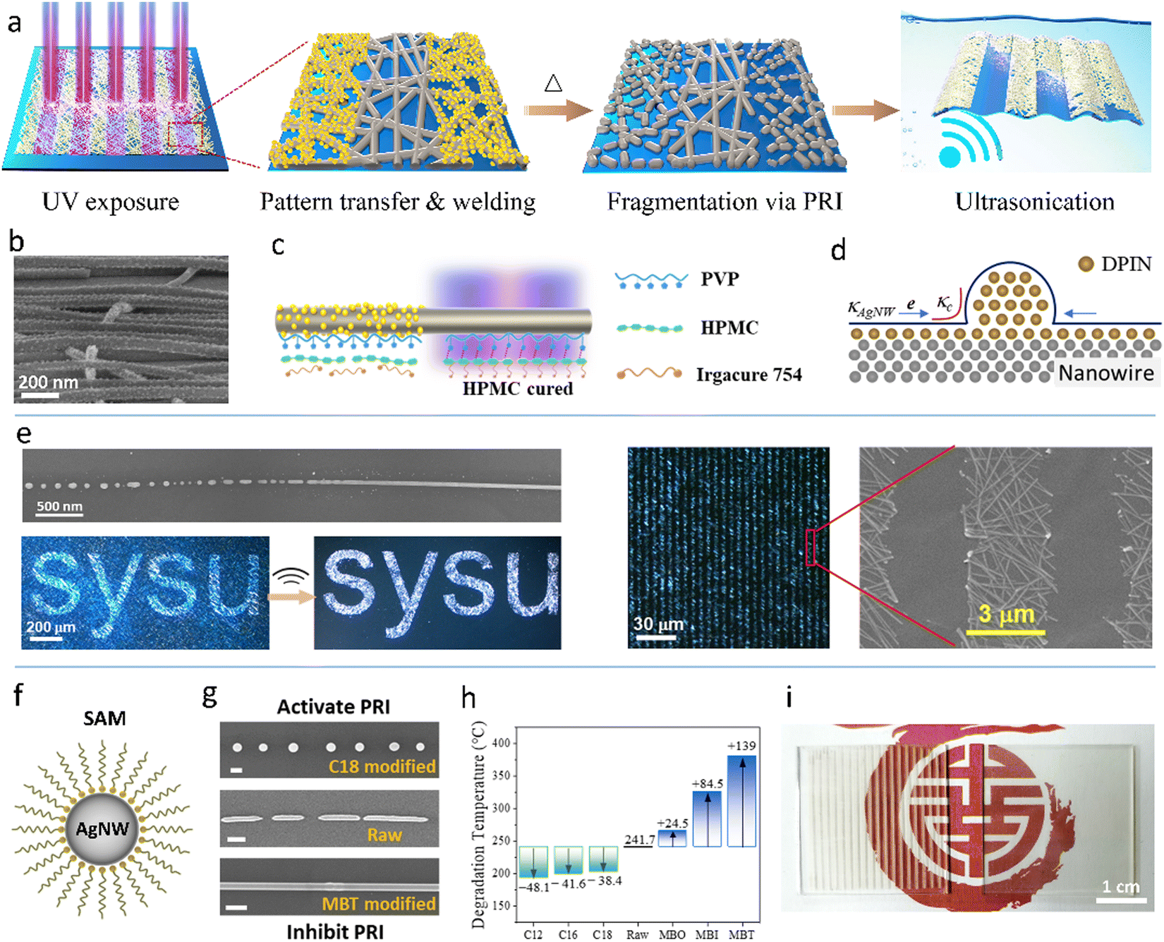 | ||
| Fig. 13 (a) PRI patterning process of the DPIN-modified AgNWs. (b) SEM image of the DPIN-modified AgNWs. (c) Schematic of selective decomposition of DPIN and curing of HPMC along a single AgNW. (d) Mechanism of DPIN NP-induced fragmentation of AgNWs. (e) SEM and OM images of the PRI-patterned AgNWs. The upper-left image of (e) is reproduced with permission.98 Copyright 2020, American Chemical Society. The other images of (a–e) are reproduced with permission.110 Copyright 2022, Springer Nature. (f) Schematic of a SAM-modified AgNW. (g) SEM images of raw, C18-modified, MBT-modified AgNWs after 300 °C annealing for 5 min. (h) Degradation temperatures of raw AgNWs and SAM-modified AgNWs. (i) Photographs of the photolithography-patterned and PRI-patterned AgNW films. Reproduced with permission.276 Copyright 2022, Springer Nature. | ||
The PRI process leads to selective fragmentation of an MNW network to disconnect the percolation way for electrons. Different from the traditional top-down and bottom-up strategies, the PRI patterning retains the traces of MNWs in the insulated area.98,110 If the PRI process does not reach the mature state and just fragments the AgNW network at junctions via the Gibbs–Thomson effect,276 the remaining traces can effectively eliminate the optical difference between the conductive and insulative regions due to the well-matched refractive indices and scattering coefficients. The difference in the transmittance is less than 10%, which makes the patterning invisible to the naked eyes (Fig. 13i).221,222,276 The invisible MNW electrode is of particular importance for display devices in terms of image quality.
4.2. Bottom-up strategy
The top-down patterning methods involve either wet or dry processes for selectively removing MNWs, which not only require expensive equipments and/or complex technical process, but also waste some MNWs. Therefore, various bottom-up patterning methods have been developed to deposit MNWs into patterns on substrates directly. These methods can be classified into three categories: printing methods, wetting–dewetting self-assembly, and template-assisted patterning.Inkjet printing. IJP is a maskless method that deposits ink droplets on a substrate to form a predefined pattern. There are two kinds of IJP: intermittent IJP and continuous inkjet (CIJ) printing.277 Intermittent IJP, also known as “drop-on-demand” IJP, directly ejects droplets to the substrate as needed, where the droplets are thermally driven or piezoelectrically driven. In CIJ printing, a continuous flow is expelled from the nozzle and then broken up into intermittent droplets through high frequency vibration,278 which are controlled by the deflection electrode to deposit into a specific position on the substrate. The patterning resolution is highly dependent on ink properties and the size of the printing nozzle. To achieve good stability, printability, and thus ultra-fine patterns, ink components (such as concentration, solvents, and other organic additives) must be carefully adjusted to optimize ink properties such as viscosity and surface tension.231,232,279–281 Coleman et al. added diethylene glycol to isopropanol dispersion to increase the viscosity of the AgNW ink, which produced reasonably uniform AgNW patterns with linewidths of 1–10 mm and a conductivity of 105 S m−1.231 Chen et al. replaced isopropanol with deionized (DI) water to provide a stable AgNW suspension, printing an AgNW electrode pattern with a linewidth of about 50 μm and an edge roughness of 5 μm on PET. Printing resolution can be further improved by reducing nozzle size. However, the nozzle is easily clogged when the material size significantly exceeds the empirically determined printable size a/50 (a is the nozzle diameter).231,232,282 Therefore, ultrasound is used to induce fragmentation of NWs to shorten their lengths, but shorter MNWs lead to lower conductivity and stretchability of the electrode. It is reported that the limitation of the ruleofthumb printable size (a/50) can be overcome using a direct printing method, in which a glass micropipette is in direct contact with the substrate through the ink meniscus (Fig. 14a). This method prints AgNWs of up to 40 μm in length into a pattern of about 270 μm in linewidth with well-defined and uniform features.283 As the traditional IJP technology faces the issue of nozzle clogging and difficulty in producing high-resolution patterns, new IJP methods, such as aerosol jet printing (AJP) and EHD printing, have been developed.
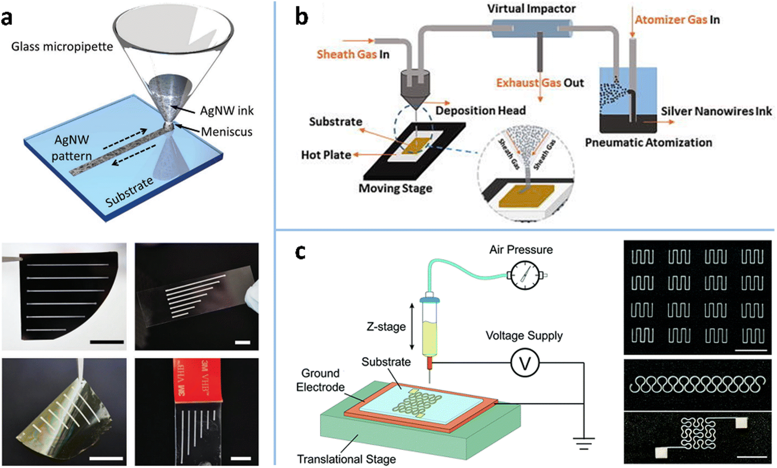 | ||
| Fig. 14 (a) Schematic of IJP for AgNWs and the printed AgNW patterns on a silicon wafer, glass slide, PI thin film, and VHB tape. Scale bars: 2 cm. Reproduced with permission.283 Copyright 2017, WILEY-VCH. (b) Schematic of an AJP system. Reproduced with permission.143 Copyright 2018, AIP Publishing. (c) Schematic of an EHD printing system and the printed AgNW patterns. Scale bar: 1 cm. Reproduced with permission.139 Copyright 2018, RSC Pub. | ||
Aerosol jet printing. AJP atomizes the functional ink to form aerosol droplets with diameters of 1–5 μm by pneumatic or ultrasonic processes and delivers the droplets to the substrate through a carrier gas (Fig. 14b).143,284 During the transportation of the aerosol, the sheath gas forms an outer layer around the aerosol stream, which prevents the aerosol particles from contacting the inner wall of the nozzle, thereby avoiding the issue of nozzle clogging. This process also shows greater ink compatibility in viscosity (0.7–2500 cP) than IJP, which is usually limited to a narrow viscosity range of 10–40 cP.285 In addition, the focusing effect of the sheath gas provides AJP with a high printing resolution of about 10 μm under appropriate conditions.286 The printing quality of AJP is closely related to the process parameters, including atomization frequency, gas flow rate, nozzle size, working distance, etc.143,287,288 It is reported that the linewidth can be narrowed by increasing the stage speed and the focusing ratio which is the ratio of sheath gas velocity to carrier gas velocity.287 Tu et al. obtained AgNW electrodes with a linewidth of 50.9 μm and an RS of 57.7 Ω sq−1 under an optimized condition (printing cycle is 1, printing speed is 0.4 mm s−1, nozzle size is 200 μm).143 AJP takes advantage of high-pressure air jets to reduce the limit on ink viscosity and aerodynamic focusing to obtain high-resolution patterns. However, some of the atomized droplets jetted by the high-pressure airflow will deposit nearby the printed patterns, resulting in rough edges of the patterns.289
Electrohydrodynamic printing. The EHD printing system consists of a pneumatic element, a power source, and a translational stage (Fig. 14c).139 The ink is delivered to the nozzle by a pneumatic press to form a meniscus which is deformed into a cone by the electrostatic repulsion of the charges induced by the electric field between the nozzle and the substrate. As the electric field stress overcomes the surface tension of the ink, a jet of droplets, with diameters 2 to 5 orders of magnitude smaller than the nozzle diameter, will be ejected from the cone.290 There are different injection modes under different electric field strength and flow rates, including dripping, cone jet, pulsating jet, and complex jet.291,292 In the “cone jet” mode, the flow rate and the electric field are properly matched, and a continuous ink stream will be ejected from the nozzle. With an excessive increase in electric field strength, “complex jet” modes (such as tilted jetting and multijetting) will be triggered and cannot be used for EHD printing. The patterning resolution can be controlled by carefully adjusting ink composition and printing parameters. Li et al. increased the printing speed from 1 to 30 mm s−1, reducing the printing linewidth from 463 to 210 μm. The best lines with a uniform shape and sharp edges were achieved at a speed of 20 mm s−1.141 Cui et al. adjusted AgNW concentration, ink viscosity, printing speed, and stand-off distance, to obtain a minimum linewidth of about 45 μm.139 An EHD-printed, aligned AgNW microgrid shows an ultrahigh T of 99.1% at an RS of 91 Ω sq−1.165 EHD printing has shown the potential for large-scale manufacture of flexible electronic devices, such as dry electrocardiogram electrodes and electronic skins.139,293,294 It can print different materials into large-scale repetitive and complex patterns with high resolution on various substrates, and has evolved from 2D to 3D micro/nanoscale additive manufacturing technology.291,293
Screen printing. Screen printing uses a squeegee to squeeze ink through a patterned screen mask to achieve large-area patterns. It is suitable for almost all types of substrates, such as textiles, PET, glass, paper, polyimide (PI), etc.295–299 The printing process can be implemented on both flat surfaces and curved surfaces (Fig. 15a and b) so that R2R printing modes can be developed to improve output efficiency.300–302 The patterning resolution of screen printing largely depends on the graph structures of screen masks and the formulation of printing inks.303,304 High-viscosity ink can easily cause clogging, while low-viscosity ink induces leakage.305 Screen printing requires the ink to have the thixotropic shear thinning property: the ink viscosity decreases with the shear rate to allow ink to pass through the mesh without congestion,234,306 and the viscosity quickly returns to its initial high value to retain the ink on the mesh (Fig. 15c),295,303,305 which improves printing precision. A shear-thinning ink is reported to consist of Cu@Ni rose-stem nanowires (RSNWs), carboxymethyl cellulose (CMC), PVP (MW = 10
000), and DI water.297 The ink viscosity is 102.2 Pa s and is reduced by about 1 Pa s as the shear rate increases to 103 s−1 (Fig. 15c). The viscosity value recovers the initial value within 100 s, providing enough time to deposit the ink onto the substrate with good printing quality. Another shear-thinning ink is the mixture of AgNWs, HPMC, and Zonyl FC-300, in which HPMC is used to adjust the rheological behavior of AgNW-ink (Fig. 15d).233,295 The ink yields neat and smooth lines with a high conductivity of 46700 S cm−1 and a minimum resolution of 50 μm.295 Besides printing single functional material, screen printing can also print composite materials.306,307 Li et al. developed a thixotropic ternary ink that combines AgNWs with GO nanosheets and hydrated ruthenium oxide nanoparticles without inert additives. A uniform pattern with a minimum feature size of ∼50 μm is directly achieved by screen printing without any hash post-processing.307 In addition to adjusting the ink formulation, the properties of the pattern can also be improved by optimizing the printing parameters such as printing speed, extrusion force, the gap between the mesh and the substrate, and the number of printing cycles.308
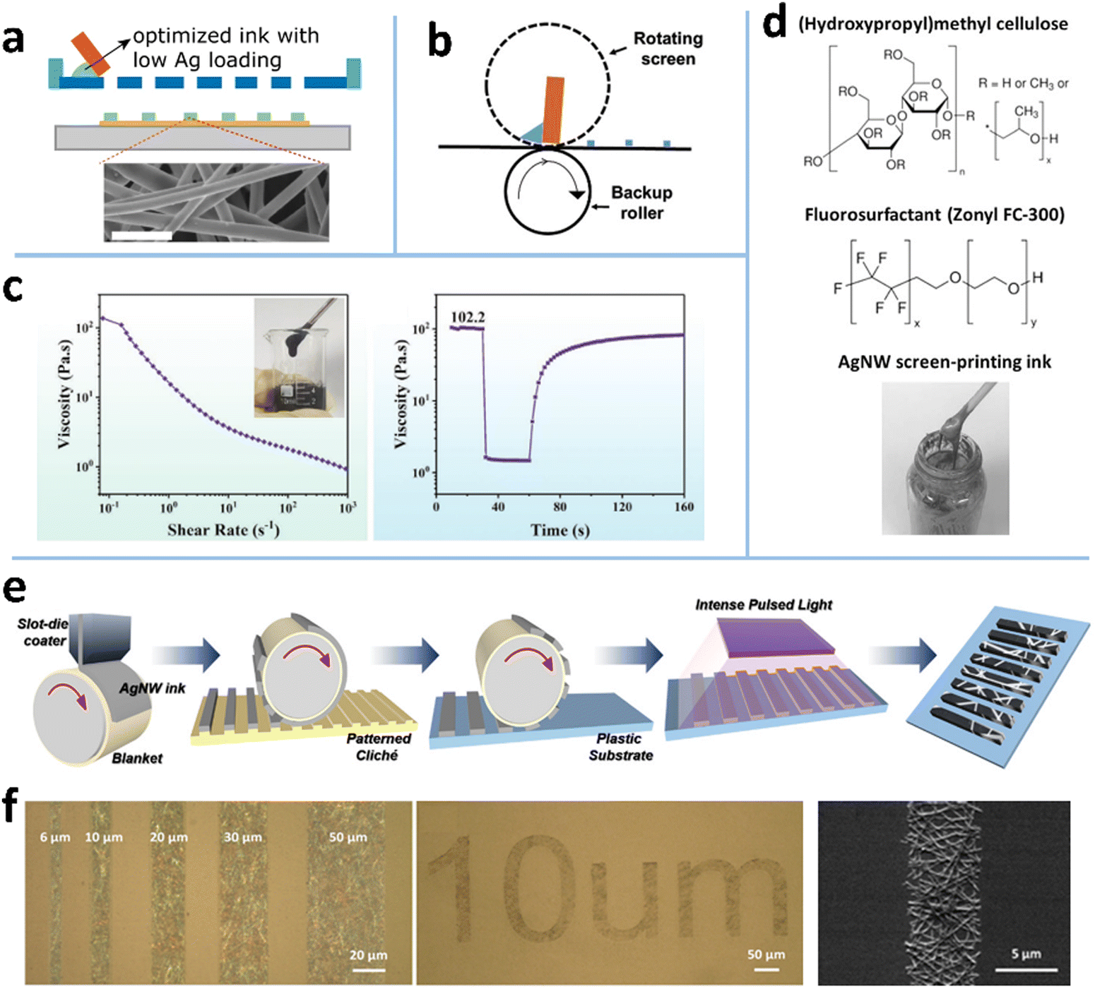 | ||
| Fig. 15 (a) Schematic of flat screen printing. Reproduced with permission.308 Copyright 2019, Springer Nature. (b) Schematic of rotary screen printing. Reproduced with permission.309 Copyright 2019, WILEY-VCH. (c) Rheological property and thixotropic behavior of the Cu@Ni RSNW ink. Reproduced with permission.297 Copyright 2020, WILEY-VCH. (d) Molecular structures of HPMC and Zonyl FC-300, and the prepared AgNW ink. Reproduced with permission.295 Copyright 2016, WILEY-VCH. (e) Process of a reverse offset printing technique for patterning AgNWs. (f) Printed AgNW patterns on plastic substrates. Reproduced with permission.239 Copyright 2019, American Chemical Society. | ||
Transfer printing. Transfer printing is controlled by the adhesion difference between two interfaces in a stamp/ink/substrate structure. Retrieval of ink occurs under stronger adhesion between the stamp and ink than that between the ink and substrate, while printing of ink occurs under weaker stamp/ink adhesion. Common methods of adhesion modulation for MNW patterning include surface chemical modification and polymer glue.310 For elastomer stamps with significant viscoelastic properties, the adhesion at the stamp interface can also be modulated by the peeling speed. A higher peeling speed facilitates ink retrieval, while a lower speed enables ink printing onto a receiving substrate.311
One advantage of transfer printing is that it separates the manufacturing substrate from the target substrate, thus overcoming the incompatibility issues of conventional manufacturing techniques for flexible polymer substrates such as high temperature and chemical etching. Another advantage is that transfer printing is compatible with the R2R process in different patterning ways, including additive transfer, subtractive transfer (see Section 4.1.2), and pattern transfer.311
The additive transfer is a process wherein the ink is first deposited on the structural stamp and then brought into contact with and delivered onto the target substrate through the stamp.312,313 In an early report, AgNWs were first deposited on the anodized aluminum oxide (AAO) membrane through vacuum filtration and then transferred onto the embossed PDMS stamp.312 The PDMS stamp was also successfully inked with AgNWs via spray coating.313 For fully transferring the AgNWs on the stamp, the receiving glass substrate was modified with 3-aminopropyltriethoxysilane which has strong σ-donating functional groups (NH2) to produce adhesion to AgNWs. As a commonly used material for stamps, PDMS needs hydrophilic treatment and suffers from temporary or permanent deformation caused by absorption of organic solvents. As a substitute, agarose has been proposed to construct stamps.236 Although the mechanical strength of agarose needs to be improved, its hydrogel properties are beneficial for transfer. An AgNW pattern of 200 × 200 μm2 has been directly transferred onto the TiO2/Ag/PES substrate through an agarose stamp, which constructs a sandwich structure of TiO2 resistive random-access memory.
Pattern transfer is the approach that combines patterning of MNWs on a donor substrate with further transferring of the pattern onto a receiving substrate.241–244,314 The key to transfer is the adhesion difference between the two interfaces, so a donor substrate with low surface energy is usually required. However, it is difficult to deposit uniform MNW networks on such substrates by the solution process. To this end, MNWs were generally deposited on porous AAO or polytetrafluoroethylene (PTFE) with low surface energy by vacuum filtration. The MNWs were then transferred onto a secondary substrate (mainly PDMS) and finally to the target substrate.315,316 Another attractive solution is that the substrate coated with MNWs was selectively modified to lower the surface energy by making use of the porosity of the AgNW networks.99,240 The AgNW patterns on the modified PDMS have been successfully transferred onto various substrates with the assistance of UV-cured epoxy resin.
Two other promising techniques for pattern transfer are gravure printing and reverse offset printing, both of which use intaglio to generate nanomaterial patterns and are compatible with the roll-to-roll process for large-area and high-throughput manufacturing.140,239,317–319 The gravure printing consists of two steps: filling ink onto the intaglio pattern and transferring the ink to the target substrate. The shape and fidelity of the printed pattern are determined by the rheological behavior of the ink defined by the capillary number (Ca = μv/σ).319 The best printing quality can be achieved by adjusting the printing speed and ink parameters (viscosity and surface tension) to make Ca ≈ 1. A water-based AgNW ink, consisting of poly(ethylene oxide), ethanol, and water, has been developed for gravure printing to generate uniform, sharp-edged lines with a resolution of 50 μm on PET.140 In reverse offset printing (Fig. 15e), the ink is first coated onto a PDMS-based blanket. The semi-dried ink on the blanket is selectively taken away by an embossed cliché. The adhesion of the ink to the blanket needs to exceed the shear strength of the edge to break the ink film and form a pattern on the blanket. The final step is the set process, in which the created patterns on the blanket are transferred onto a receiving substrate. AgNW patterns with a minimum linewidth of 6 μm have been achieved by carefully adjusting the ink composition and printing parameters (Fig. 15f).239
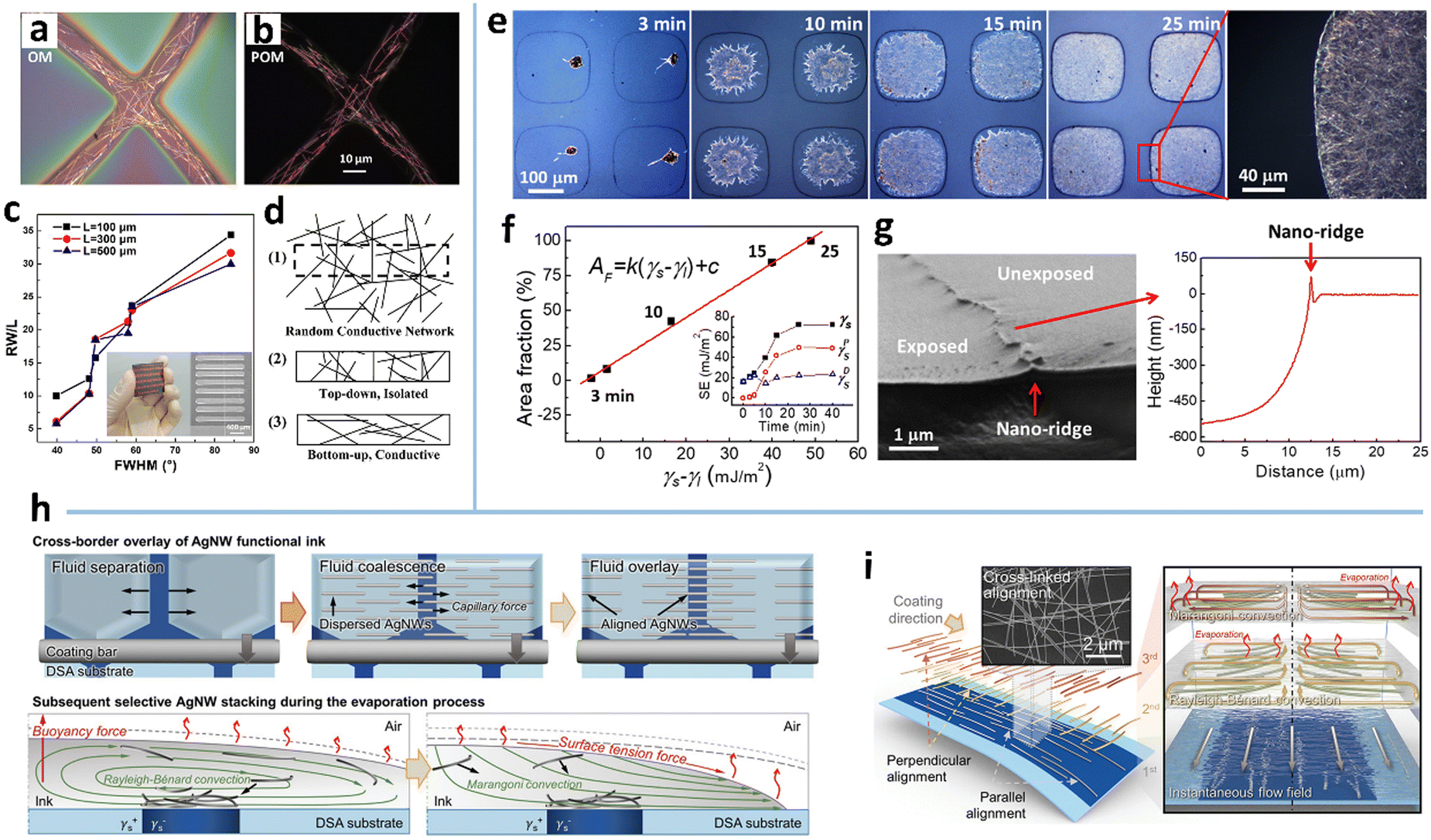 | ||
| Fig. 16 (a) OM and (b) polarizing OM images of patterned AgNWs in super-hydrophilic microchannels. (c) Variation in RW/L versus FWHM of the aligned AgNWs in the microchannels. W is the channel width and L is the channel length between electrodes. The inset is an electrode sample. (d) Schematic of the NW networks patterned by top-down and bottom-up methods, respectively. Reproduced with permission.151 Copyright 2015, American Chemical Society. (e) The effect of UV treatment time on the area fraction of AgNWs in the hydrophilic region. (f) Area fraction of AgNWs as a function of γs − γl; the inset is the surface energies (SE) for different UV treatment times. (g) SEM image of the UV-patterned PDMS and the surface scanning profile of the PDMS. Reproduced with permission.99 Copyright 2016, RSC Pub. (h) Selection deposition of AgNWs on the hydrophobic (γs−) region through Rayleigh-Bénard convection and Marangoni convection. (i) Schematic and SEM image of the multi-alignment during the coating and self-assembly process. Reproduced with permission.323 Copyright 2022, WILEY-VCH. | ||
The pattern morphology of MNWs is closely related to the coating method, wettability contrast, and topographic structure. Rod coating with high speed (e.g., >3.2 mm s−1) can yield AgNW patterning with narrow linewidths; however, there are many residual AgNWs on the narrow spacings due to the meniscus pinning and on the huge open hydrophobic regions due to fracture of the liquid film.90 In addition, the coffee-ring effect in the large-area hydrophilic region results in a lower RS. Reducing the rod-coating speed (e.g., <0.4 mm s−1) makes the meniscus follow the rod without pinning, which improves the electrode conductivity and patterning resolution down to 20 μm in spacing.324 Nevertheless, there are still residual MNWs on the hydrophobic region. Our group achieved a high-resolution, uniform AgNW pattern without residual AgNWs in the hydrophobic region by spin coating the AgNW ink in a wettability-patterned PDMS (Fig. 16e).99 Large centrifugal force at high rotation per minute can overcome the ink hysteresis on hydrophobic regions and the pinning effect on patterned hydrophilic regions to remove excess ink and achieve uniform deposition. In addition, wettability contrast plays a vital role in the morphologies of self-assembled MNWs. In the patterned region, high surface energy (e.g., >72 mJ m−2) is required to obtain positive spreading coefficients for the ethanol-dispersed AgNW ink and thus achieve high-fidelity patterning.99 The area fraction of AgNWs in the hydrophilic region is found to be linearly proportional to γs − γl (γs and γl are the surface energies of the hydrophilic region and ink) (Fig. 16f). γs − γl of 49 mJ m−2 is required to achieve 100% area fraction, that is, full-coverage and high-resolution patterning. It is also found that the UV/O3-patterned PDMS has nanowell-like topography. This structure induces strong pinning of the ink to establish a well-defined, smooth, and continuous percolative path along the patterning boundary (Fig. 16e and g).
Instead of dewetting self-assembly, microflow velocity-field-induced patterning of MNWs has been recently reported on a patterned substrate with a less wettability contrast through bar coating (Fig. 16h).323 A cross-border overlaying of the ink was formed on the substrate, where the ink flow decelerates at the surface with low surface energy and accelerates at the surface with high surface energy. Therefore, the AgNWs in the ink can be layer-by-layer assembled on the hydrophobic region (γs−), with the 1st layer of AgNWs aligned along the coating direction, and the 2nd and 3rd layer of perpendicularly aligned AgNWs driven by Rayleigh–Bénard convection and Marangoni convection respectively, giving rise to a cross-linked AgNW network (Fig. 16i).
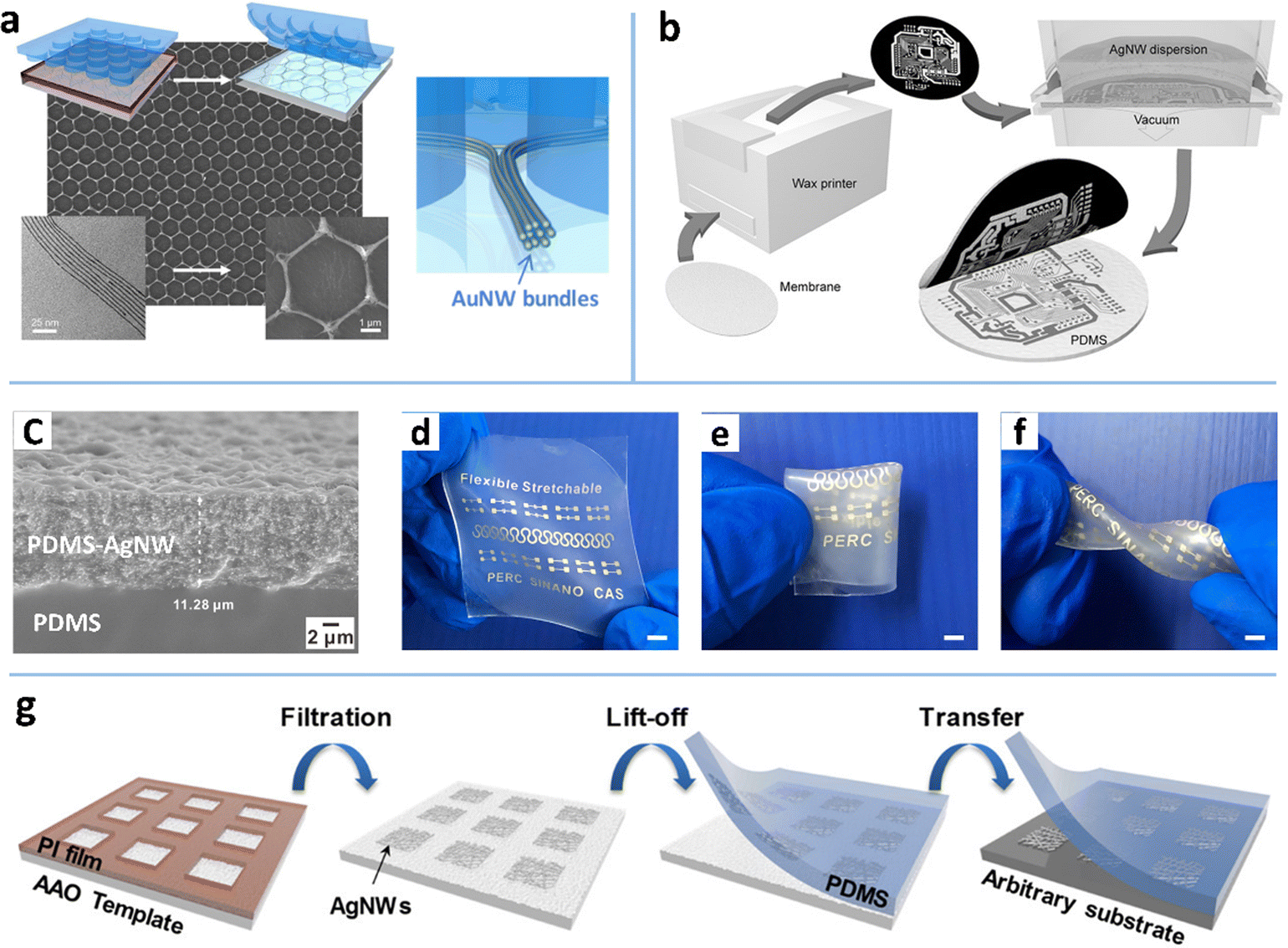 | ||
| Fig. 17 (a) Schematic of the nanoimprinting and bundling process, and SEM and TEM images of the patterned AuNWs. Reproduced with permission.108 Copyright 2016, American Chemical Society. (b) Process of a wax printer and vacuum filtration-based patterning method for AgNWs. Reproduced with permission.328 Copyright 2015, WILEY-VCH. (c–f) SEM image and photographs of the stretchable, embedded AgNW patterns that are fabricated by a vacuum filtration and transfer process. Reproduced with permission.329 Copyright 2022, Springer Nature. (g) Schematic of the AgNW patterning process through vacuum filtration and transfer printing. Reproduced with permission.316 Copyright 2020, American Chemical Society. | ||
A combination of hollow-out masks and vacuum filtration is another strategy for MNW patterning. Vacuum filtration uses negative pressure to accelerate the filtration of the MNW ink through a hollow-out mask to achieve an MNW pattern. The deposited patterns on filter membranes are generally transferred to target substrates for further use.330 For this reason, the hydrophobic filter membranes made of polyvinylidene fluoride (PVDF) and PTFE are frequently used to allow pattern transfer.331,332 The AAO film has also been used as the filter membrane, on which the AgNW pattern can be transferred onto the PDMS film with the assistance of DI water or after modifying AAO with octadecyltrichlorosilane.243,316 Also, uncured or semi-cured PDMS films are used to transfer and carry AgNW patterns from the filter membranes. The AgNWs are embedded in PDMS to form SEs with stretchability up to 100% (Fig. 17c–f).329
In this method, the mask is paramount to patterning quality of MNWs. Removable hollow-out masks are the most used. However, there are some disadvantages of hollow-out masks. First, the patterning resolution is usually poor for the following reasons: (1) it is difficult to fabricate and handle a thin mask with a high-resolution pattern. (2) Lateral penetration between the mask and the substrate and NW crossover between the open area and the mask surface leads to the rough edges of the pattern. Um et al. patterned an ultrathin PI film by photolithography and RIE processes to obtain a high-resolution mask.316 The ultrathin PI masks can conformally adhere to the AAO filtration membrane and be intactly removed, producing clear AgNW patterns with a minimal linewidth of about 3.5 μm (Fig. 17g). Second, the hollow-out masks are not suitable for preparing complex patterns with closed-loop areas, because the mask is difficult to be peeled off from the filtration film in one step. To address the above issues, two kinds of masks have been developed. One is the 3D PDMS mask that allows the AgNW ink to flow through the channels inside it, achieving a closed-loop pattern with sharp edges.333 The limitation of this method is the difficulty in fabrication of high-resolution 3D masks. The other one is the blocking mask that is directly printed on porous filters. In early reports, a black ink was patterned on a paper through screen printing to block the paper selectively. After vacuum filtration, a paper-based AgNW circuit was achieved with a high conductivity of 60781 S cm−1 and a minimal linewidth of 250 μm.334 Another facile method resorts to a wax mask that is printed on the hydrophilic porous PVDF film by a desktop wax printer (Fig. 17b).328 The AgNW ink is spontaneously filtered through the masked PVDF membrane to form AgNW patterns with a minimum patterning size of approximately 100 μm, which is limited by the resolution of the wax printer. Similarly, through screen printing, liquid PDMS is also patterned on filter membranes (Teflon and PTFE). A hydrophobic mask can reduce the AgNWs remaining outside the defined pattern due to the dewetting effect, which yields a pattern with sharp edges and a linewidth down to 50 μm.315,328
In short, the patterning technology for MNWs has made considerable progress since 2015. As shown in Table 2, the highest patterning resolutions of 250 nm for AuNWs, 3 μm for AgNWs, and 13.5 μm for CuNWs have been achieved. Among the top-down patterning strategies, photolithography can fabricate AuNW patterns with the highest resolution of 2.5 μm; some etching-free methods based on adhesion difference have been developed with patterning resolutions down to 10 μm; the novel PRI-based patterning method, different from the traditional top-down and bottom-up strategies, gives rise to the highest resolution of 3 μm in both linewidth and spacing for AgNW microelectrodes. As for the bottom-up strategies, the printing resolutions of IJP, AJP, and screen printing have been improved to 50 μm. The template-assisted patterning methods such as vacuum filtration have reduced the patterning linewidth to <10 μm. They have the merits of material saving and easy operation but are impractical for large-area manufacture. It is noted that the reverse offset printing shows high resolution and good manufacturability.
| Technical route | Methods | Materials | Substrates | L W (μm) | S (μm) | Ref. |
|---|---|---|---|---|---|---|
| a PUU: polyurethane urea. b PC: polycarbonate. | ||||||
| Top-down | Photolithography | AgNWs | Glass, PDMS | 20 | 40 | 206 |
| Photolithography and transfer | AgNWs | PDMS and PUUa | 100 | 100 | 335 | |
| Shear alignment and photolithography | AuNWs | Si wafer | 2.5 | — | 336 | |
| Photolithography | AgNWs | Glass | 180 | 110 | 337 | |
| Photolithography | AgNWs and RuO2 | PET | 10 | — | 338 | |
| Atmospheric cold plasma-jet | AgNWs | PET | 50 | — | 339 | |
| Dry-film photolithography | AgNWs | PET | 10 | — | 212,213 | |
| Microcontact printing and etching | AgNWs | Si, PET | 25 | 25 | 265 | |
| Selective adhesion and transfer | AgNWs | PMMA, PET, acrylic substrates | 100 | — | 106 | |
| IJP and selective removal | AgNWs | PET | 60 | 80 | 218 | |
| IJP and adhesion manipulation | AgNWs and PMMA | Glass, PET, PDMS | 10 | 10 | 238 | |
| IJP and selective removal | AgNWs and PEDOT:PSS | Glass, PEN | 30 | — | 235 | |
| Selective adhesion and ultrasonication | AgNWs and TEH | PDMS | 30 | 10 | 37 | |
| IPL and selective removal | AgNWs/CuNWs | PET, cPI, PEN, PC | 13.5 | — | 219,220 | |
| Selective DUV exposure and thermal annealing | AgNWs and IZO | Glass, PI | 100 | 100 | 223 | |
| PRI patterning | AgNWs and DPIN | Glass, PDMS | 3 | 3 | 110 | |
| Laser scanning and transfer | CuNWs and PUA | Adhesive substrate | 100 | — | 259 | |
| Laser scribing and heat press lamination | AgNWs | Textile | 135 | — | 340 | |
| Laser ablation | AgNWs/CuNWs | Glass, silicon, PDMS, PET | 20 | — | 227,230,341 | |
| Laser ablation | AgNWs and PEDOT:PSS | PI | 100 | 100 | 228 | |
| Bottom-up | AJP | AgNWs | Glass | 50.9 | — | 143 |
| Gravure printing | AgNWs | PET | 50 | 100 | 140 | |
| IJP | AgNWs | Si, glass, PI, VHB tape, PDMS, PET, photo paper | 240–270 | — | 232,283 | |
| IJP | AgNWs | PET | 50 | — | 83 | |
| Screen printing | AgNWs | PET, PUA, glass, PDMS | 50 | 50 | 233,295,342 | |
| Reverse offset printing | AgNWs | PC,b PET | 6 | 30 | 239 | |
| Wetting–dewetting | AgNWs | Silicon | 8 | — | 151 | |
| Wetting–dewetting and transfer | AgNWs and PEDOT:PSS | Glass, PDMS | 150 | — | 241 | |
| Wetting–dewetting and transfer | AgNWs | PDMS, PVA, paper, PET | 20 | — | 99,244 | |
| Template assisted method | AuNWs | Glass, PET | 0.25 | 5 | 327 | |
| Template assisted method | AgNWs | Glass, PI | 10 | 50 | 325 | |
| 2D ice-templating approach | AgNWs | PET | — | 100 | 36 | |
| Vacuum filtration and transfer | AgNWs | PDMS, PET | 100 | 100 | 328,333 | |
| Screen printing and vacuum filtration | AgNWs | PTFE | 50 | 50 | 315 | |
| Vacuum filtration and transfer | AgNWs | Si, glass, PET | 3.5 | — | 316 | |
5. Applications
MNWs assembled into specific morphologies have shown great potential in diverse fields, including electronics, photonics, optoelectronics, catalysis, etc.43,44,343 Since there are too many novel devices and application scenarios for this review to cover, we focus on a few distinguished applications which are based on TEs and SEs. The properties of TEs and SEs fabricated by the methods of self-assembly, alignment, and patterning are investigated, compared, and discussed, to provide guidance for fabricating high-performance devices.5.1. Flexible transparent electrodes and applications
 | (5) |
 | (6) |
 | (7) |
 | (8) |
Haze is another critical parameter for application in displays, touch panels, lighting, and solar cells. It refers to the degree of deviation of light when passing through MNW networks:348
 | (9) |
 | (10) |
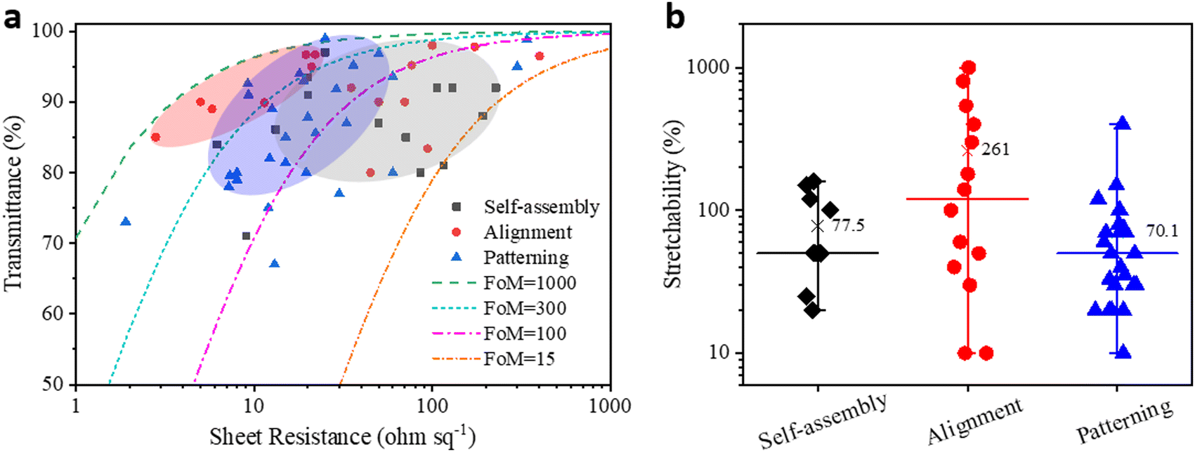 | ||
| Fig. 18 (a) Transmittance versus sheet resistance of the MNW-based TEs fabricated by self-assembly,34,36,45,47–49,108,131,134,327,353–357 alignment,12,28,29,53,77,79,81,86,88,91,95,96,102,161,170,358,359 and patterning methods.37,105,145,216,217,219,220,223,230,234,238,241,244,249,259,262,263,281,305,308,314,315,317,324,335,340,360–364 The dotted lines derived from eqn (6) denote the performances at different FoMs. (b) Stretchability of the MNW-based SEs fabricated by self-assembly,34,36,124,131,365–371 alignment,29,77,82,87,89,167,358,372–376 and patterning methods.37,139,232,244,251,259,283,293,308,315,317,340,361 | ||
LEDs. The performances of different LEDs have been improved by assembling MNWs into specific structures. One structure is bi-aligned MNW networks which enhance the external quantum efficiency (EQE) of quantum dot LEDs (QLEDs) and organic LEDs (OLEDs) through alignment-enhanced FoMs.86,227,378 The EQE of a reported OLED with an aligned AgNW TE is 20% higher than that of a reference device with an ITO electrode.378 The EQE of the QLEDs is enhanced by a factor of 7 compared to the QLED with a random AgNW network.227 Due to the improved uniformity of the bi-aligned AgNW network, a QLED with 30 μm linewidth is lighted by a laser-patterned AgNW electrode.227 Another structure for LED improvement is MNWs with pattern designs. A nanopatterned AgNWs/ZnO TE was used to enhance the light outcoupling of green-emitting perovskite LEDs, achieving a high EQE of 24.5%.379 With the inherent stretchability of AgNW networks, serpentine AgNW electrodes effectively reduce local strain, improving the bending stability of OLEDs.380
Solar cells. As in LEDs, MNW alignment finds application in organic solar cells (OSCs), in which enhanced FoMs account for the improvement of power conversion efficiency (PCE).86,359,378 In an interesting report, aligned AgNWs were decorated with SiO2 NPs to enhance electric field intensity at NP–NW interfaces through a strong gap-plasmon effect (Fig. 19a and b), which improves the Jsc value and EQE and achieves a PCE of 9.19% in the OSCs (Fig. 19c–f).377 A cross-aligned AgNWs/polyester-based TE induced a large-grained perovskite film, which imparts a perovskite SC with a PCE of 17.51%.381 Patterned MNWs improve the PCE of solar cells by enhancing transparency and the light trapping effect.105 Multi-length scale AgNW grids provide OSCs with a PCE of 9.02%, higher than that of the AgNW uniform film-based solar cell.105 A nanoimprint-AgNW mesh not only has high FoMs (335), but also induces light-trapping through the light scattering from NWs to increase optical absorption of OSCs.382
 | ||
| Fig. 19 (a) Schematic of the SiO2 NP-decorated, aligned AgNWs and (b) the plasmon coupling between the NP and AgNW. (c) Schematic of an OSC device with the aligned NP–AgNW electrode and (d) the energy level diagram. (e) J–V curves and (f) IPCE spectra of the OSCs with different TEs. Reproduced with permission.377 Copyright 2018, WILEY-VCH. (g) Schematic of the force-sensitive TP with bi-aligned AgNW TEs. (h) Normalized luminance at 448 nm versus the writing force. (i) Digital photographs of color change on the TP versus different writing forces. Reproduced with permission.91 Copyright 2017, American Chemical Society. | ||
Touch panel. A touch panel (TP) is based on either a uniform or a patterned TE. For the former, researchers developed high-performance MNW TEs with emphasis on enhancing FoM and uniformity.34,91,134,255,383 Highly cross-aligned AgNW networks were fabricated by Meyer-rod coating combined with electrostatic adsorption, which showed a high FoM (Π = 479, n = 0.12) and a small standard deviation (1.2) of RS and were used for the construction of a four-wire resistive-type TP (RTP) (Fig. 19g–i).91 By using a coffee-ring self-assembly method, Xiong et al. prepared porous AgNW networks with a low RS (25 Ω sq−1) at a high T (97%) for surface capacitive TPs (SCTPs).34 The disadvantage of RTPs and SCTPs is that they cannot realize multi-touch. To sense multi-touch, patterned electrodes are required to construct projected capacitive TPs (PCTPs). Using an etching-free photolithography method, Shin et al. fabricated an AgNW-based PCTP which consisted of one glass and two flexible AgNW films (GFF).264 Cann et al. utilized laser patterning to fabricate a single-sided, single-layer AgNW-based PCTP on a glass substrate (OGS).226 Our group used laser ablation to fabricate a single-sided, embedded AgNW-based flexible PCTP on PET, demonstrating multi-touch.
5.2. Stretchable electrodes and applications
Fig. 18b shows the stretchability distributions of the MNW SEs which are catalogued according to the three types of assembling methods. Nearly all of the data are from 2D film-shaped SEs. Most self-assembled SEs have stretchability in the range of 20–160%, with an average value of 77.5%. A 2D porous Au mesh on a prestrained PDMS is reported to have a stretchability of up to 160%.368 The largest stretchability of 800% is obtained by a 3D AgNW-hydrogel aerogel with a cellular structure which is fabricated by the freeze-drying self-assembly method.109 The patterned MNW-based SEs have more widespread stretchability, spanning from 10% to 400%. The stretchability of the in-plane MNW meshes is generally less than 150%. One outstanding MNW structure with a stretchability of >400% is the kirigami-engineered AgNW SE which is patterned by a UV laser.387 The kirigami design can effectively reduce strains in MNW networks through 3D buckling under large tensile deformation at the device level, so that the AgNW SE under strains of 0–400% exhibits only a 3% change in resistance. As for aligned MNW networks, the stretchability spans from 10% to 1000%, with an average value of 261%. Two representative aligned MNW SEs are the horizontally aligned AgNW nanomembrane and the vertically aligned enokitake-like AuNW microfilm, which are fabricated by a modified LB assembly and a modified seed-mediated electroless plating method, respectively.87,388 They possess stretchabilities of up to 1000% and 800% respectively, which are the highest-ranking stretchability values ever reported for MNW-based SEs.
In brief, the MNW SEs fabricated by self-assembly, alignment, and patterning methods have demonstrated high stretchability in the ascending order by discrete degree: aligned MNWs > patterned MNWs > self-assembled MNWs. The stretchability of self-assembled and patterned MNW networks with in-plane structures is mainly in the range of 10–150%, with the majority having a stretchability lower than 100%. The MNWs, which are with 3D structures or can induce out-of-plane deformation, have a higher stretchability of >200%.109,387 By contrast, the aligned MNW networks can effectively dissipate the applied strain to provide the highest stretchability with a broad distribution of 10–1000%. Since the advanced MNW SEs assembled by the three methods have a stretchability of >100% which is enough to accommodate skin deformation,389 various skin-mountable optoelectrical devices have been developed.
Resistive strain sensors. MNW-based resistive strain sensors typically consist of MNW electrodes and elastomers. The MNW SEs are the sensing units, the performance of which is mainly characterized by stretchability, sensitivity, linearity, etc. The sensitivity is quantified by the gauge factor (GF):
 | (11) |
The structures of MNW SEs have an essential influence on the performance of strain sensors. There are three patterned structures for performance enhancement: (1) patterning MNWs into micro-lined electrodes. A micropatterned AgNW–acrylate SE with a narrow linewidth can evade the Poisson compression effect through the formation of parallel cracks (Fig. 20a),37 which enhances the GF (3.2 × 107) by 200 times as compared to that of the corresponding bulk film, with a transparency of 90.3% and a maximum stretchability of 20%. High sensitivity enables the sensor to clearly detect the percussion (P), tidal (T), and diastolic (D) waves and dicrotic notch of the wrist pulse at a high signal-to-noise ratio (Fig. 20b and c), so that the comprehensive medical parameters including augmentation index, transit time, and K value can be estimated from the pulse signals. (2) Patterning the substrate into meshed structures. A circle-meshed substrate can redistribute the stress uniformly and induce cracks in the AgNW network without total disconnection, giving rise to a high GF of 846 with a large strain range (150%) and a high transmittance (88.3%).397 (3) Patterning MNWs and the substrate. An AgNW mesh is formed in a square plate array with concave channels, which induces stress concentration in the concave lines.398 As a result, a large GF of 150000 with a large stretchability of 60% and a good linearity of R2 = 0.989 is achieved, which is able to detect the full-range human body motions.
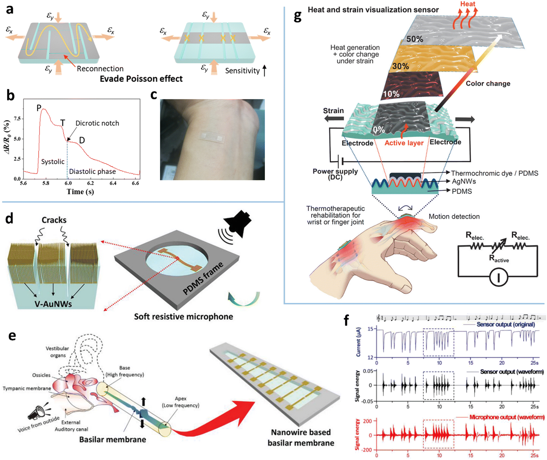 | ||
| Fig. 20 (a) Schematic of GF enhancement by changing crisscross cracks in a bulk AgNW film to parallel cracks in the patterned AgNW–acrylate composite. (b) Resistance signal of wrist pulse. (c) The AgNW–acrylate based strain sensor on the wrist. Reproduced with permission.37 Copyright 2020, American Chemical Society. (d) Schematic of the soft resistive microphone and v-AuNWs film. (e) Schematic illustration of the human ear with an uncoiled cochlea and the artificial basilar membrane made of eight cracked v-AuNW strain sensors. (f) Sensor output, detection, and commercial microphone waveform in response to a piece of music. Reproduced with permission.399 Copyright 2020, WILEY-VCH. (g) Schematic of the thermotherapeutic patch integrated with a strain sensor and a thermochromic layer and its working mechanism. Reproduced with permission.400 Copyright 2020, WILEY-VCH. | ||
Aligned architectures have been reported to effectively increase the stretchability of MNW SEs to >300%.87,373,375 However, uniform aligned films usually exhibit low GFs of less than 10.388 A vertically aligned AuNW (v-AuNW) film patterned with pinholes can cause a 3.1-fold increase in the GF (28.6) compared to the counterpart without patterned holes.365 The detected pulse signal shows four times enhanced amplitude with clear systolic, diastolic, and notch peaks. The enokitake-mushroom-like v-AuNWs are also combined with the cracked Au film, which enhances the GF from 0.17 to 1023 in the strain range of 0–20%.401 The v-AuNWs with local cracks, as a resistive acoustic sensor, have ultrahigh acoustic sensitivity and can detect the waveform of musical notes with distinguishable frequencies, which is comparable to that of a commercial microphone (Fig. 20d–f).399 A soft artificial basilar membrane is constructed by integrating the eight acoustic sensors on a flexible trapezoid frame (Fig. 20e), which achieves high-frequency selectivity in the range of 319–1951 Hz with a high sensitivity of 0.48–4.26 Pa−1.
Self-assembly of AgNWs onto a wrinkled PDMS, as a strain sensor, provides larger stretchability.400 The AgNW strain sensor is further integrated with a thermochromic dye to construct a user-interactive thermotherapeutic device (Fig. 20g). The thermochromic film on the strain sensor with the same current bias can cause a color change under different tensile strains. The self-assembled, wrinkled AgNW SE endows the device with a high stretchability of 100% and linear sensitivity. This device can be used for the precise rehabilitation of injured tissues through strain-controllable and color-visible heating.
Epidermal electronic sensors. Epidermal electronics refer to ultra-thin electronic devices with a thickness less than tens of microns that can adhere to the skin comfortably and imperceptibly. MNWs are generally assembled into specific structures to construct strain-insensitive SEs which are ideal building blocks for such devices. The vertically aligned AuNW film with a thickness of 300 nm has a low GF of 0.17 within 20% strain.401 A “stick-and-play” gold E-tattoo with multifunction is realized by combining the AuNWs with a tattoo transfer technique. It successfully detects the physiological signals of strain, strain direction, pressure, temperature, and glucose/lactate levels. Using the BF method and laser ablation, Zhu et al. reported a porous, epidermal SE with a thickness of 4.6 μm (Fig. 21a).133 This SE is totally reversible within 15% strain after the first stretch. The high-conductivity, air permeable, ultrathin, embedded structure endows the SE with excellent stability and low impedance. The detected ECG signal has a comparable SNR (7.0 dB) to that (7.1 dB) of the commercial gel electrode (Fig. 21b). The AgNW thin film with a kirigami pattern exhibits a <3% change in resistance under 0–400% strain.387 Long-term monitoring of bioelectrical signals is achieved after selectively passivating the AgNW kirigami. Surface electromyogram (sEMG) signals from the left and right arms are used for command classification based on their root-mean-square values, which successfully realizes the flight manipulation of a quadrotor drone (Fig. 21c–e). In addition to detecting biopotential signals, MNWs can also construct a self-powered electronic skin, where nanofiber templated AuNWs are the intermediate electrode between the substrate and the dielectric layer made of microscale cracked chitosan membranes (Fig. 21f–h).402 The fabricated single-mode triboelectric nanogenerator exhibits a pressure sensitivity of 0.012 kPa−1 in the range of 0 to 70 kPa and can be used as an epidermal touch/pressure sensor (Fig. 21i).
 | ||
| Fig. 21 (a) OM image of the patterned porous AgNW electrode on skin. (b) ECG spectra monitored by the porous AgNW electrode and gel electrode. Reproduced with permission.133 Copyright 2020, American Chemical Society. (c) Configuration of the transparent kirigami electrode (TKE)-based sensor. (d) sEMG signals from the TKEs on the left/right arms. (e) Schematic of flight manipulation of a drone with the TKEs. Reproduced with permission.387 Copyright 2019, American Chemical Society. (f) Photograph of the AuNW/chitosan-based electrode on skin. (g) SEM image of the AuNW cross-section. (h) Device structure of the e-skin. (i) Output voltage and current curves of the e-skin under cyclic touches. Reproduced with permission.402 Copyright 2022, WILEY-VCH. | ||
6. Conclusions and perspectives
MNWs with the 1D inherent structure are ideal transport materials for electrons, photons, phonons, etc. Assembling MNWs into macroscale architectures manifests or further enhances these transport properties, which breeds and expedites many discoveries and novel applications, such as the newly flourishing stretchable electronics. So far, great strides have been made in the morphology manipulation of MNWs with diverse assembly strategies since the turn of the century. In this review, the main strategies for the assembly of MNWs have been summarized, including the self-assembly methods that spontaneously organize MNWs into a specific regular geometric appearance, the alignment methods which deposit MNWs into an anisotropic architecture with one or more aligning directions, and the patterning methods which process MNWs into well-designed structures. Each assembly method has its merits and limitations, which are summarized in Table 3. And the progress, main features, and key issues of these methods are also highlighted below.| Methods | Merits | Limitations |
|---|---|---|
| Self-assembly | ||
| Coffee-ring effect | Dynamic control over MNW deposition; mass manufacture; compatible with various materials | Requires substrate modification; high haze as TE; impractical in fabrication of 3D structures |
| Ice templating | Versatility in porous structures; simplicity; distinct physico/mechanical attributes | Requires freeze drying and posttreatment to improve performance; special setup |
| Breath figure | Low-cost; time-saving; easy implementation | Limitations in the sizes of the pores; poor control of the surface morphology |
| Alignment | ||
| Bubble blowing | Simplicity; low-cost; compatible with various substrates; high alignment degree | Difficult to achieve high-density NW deposition; low performance; poor manufacturability |
| Shear flow | Simplicity; large area; low-cost; good manufacturability | Moderate alignment degree |
| Printing | High positional control; high alignment degree | Special setup; impractical for large-area manufacture |
| Electrospinning | High alignment; large areas; high position control | Requires posttreatment to remove the polymer matrix; lower conductivity |
| LB technique | Ultrahigh alignment; compact deposition; high electromechanical performance | Rigid condition control; requires surface modification and transfer process; time-consuming |
| Electromagnetic field | Facile and precise control; long ranged; non-contact forces | Small forces in microscale and nanoscale; requires auxiliary electrodes, uniformity in NW length, or surface modification |
| Patterning | ||
| Photolithography | Mature industrial technology; high resolution | Complex process; expensive equipment; environmentally unfriendly |
| Etching-free lithography | Environmentally friendly; low cost; large-area production | Requires elaborate tailoring of MNW inks and interfaces to achieve adhesion difference |
| Laser ablation | Designable patterns; non-contact; mask-free | Potential damage to the substrates; low productivity; expensive equipment |
| PRI method | High resolution; low visibility of patterns | Requires high-temperature annealing; surface modification |
| IJP/AJP/EHD printing | Noncontact; mask-free; material saving; designable patterns | Nozzle clogging; moderate resolution |
| Screen printing | High productivity; controllable deposition; easy implementation | Easy clogging of screen mesh; moderate resolution |
| Reverse offset printing | High resolution; large-area manufacture | Complex process; expensive equipment; high pressure |
| Wetting–dewetting | High resolution; complex patterns | Surface modification; lab scale fabrication; residual NWs in unpatterned regions |
| Mask-assisted methods | Material saving; simple; low cost | High requirements for mask; rough edges; difficult to fabricate complex patterns |
The self-assembly of MNWs generally yields two types of structures: 2D porous networks and 3D foamy structures. The 2D porous films used as TEs and SEs are reported to have higher optoelectrical performance and stretchability than disordered MNW networks. However, their FoM values are generally less than those of aligned and patterned MNW networks (Fig. 18a). In addition, the NW bundles induced by the self-assembly process increase the haze of the networks due to increased scattering cross-section, which is disadvantageous for application in touch panels and displays. The self-assembled MNW TEs with high hazes may be better suited for solar cells, which deserves further research. Besides, we believe that the self-assembled MNW micromeshes have great potential in permeable conductors for wearable on-skin electronics. As for 3D structures, the most amazing architecture of MNWs is the aerogel that combines the merits of MNWs and aerogels, exhibiting unparalleled potential in electrocatalysis, sensing, and plasmonics. For instance, an AgNW aerogel combined with a hydrogel shows a superhigh stretchability of 800%. So far, more attention has been paid to constructing new structures or pursuing high performance, while the in-depth study of formation mechanisms for MNW aerogels is lacking.403
Aligned MNW assemblies with a single direction and multi-direction have been realized by various methods. Based on the driving force, these methods can be categorized into shear flow-induced alignment, LB techniques, and electromagnetic field methods. The shear force-based methods have the advantages of being a simple process and being compatible with the R2R process, the LB techniques enable compact MNW assembly with an ultrahigh alignment degree, and the electromagnetic field methods show facile and precise manipulation of MNW deposition via distribution, strength, and frequency of the applied electromagnetic field. In terms of scalability, the rod/bar/blade (with or without a structured surface) coating methods are the most feasible methods; however, the alignment degree of the methods is unsatisfactory. In addition, the patterned, aligned array of MNWs that calls for the positional control of the NWs on the substrates is unable to be achieved by the simple rod/bar/blade coating methods. Modified rod/bar/blade coating methods or a combination of a few existing approaches still hold considerable appeal.
Well-defined, high-resolution MNW patterns have been fabricated on different substrates through various top-down and bottom-up strategies. Besides the etching-based photolithography and laser ablation, the etching-free top-down methods based on the adhesion difference and PRI have come out recently with patterning resolution down to 3 μm for AgNWs. To simplify the patterning process, novel bottom-up strategies such as IJP and wetting–dewetting self-assembly have been rapidly developed recently. The linewidth has been lowered to <50 μm for IJP and to 3.6 μm for vacuum filtration-based patterning. Still, several significant challenges remain. First, narrower linewidths of MNW networks lead to large variation in resistance among the electrodes with the same size. A conductive composite would be a good solution, which needs further studies. Second, for AgNW and CuNW-based TEs, patterning traces are easily visible to the naked eyes due to their strong scattering in the visible wavelength range, which hinders the commercialization in displays and touch panels. Semi-etching and thermal fragmentation can reduce the patterning visibility but also complicate the patterning process. Further work is still needed to resolve this issue in a simple manner.
Manipulating MNW assembly have already proven to enhance performance and offer new features for various devices. However, most studies just provide demonstrations or proof of concept. A scalable assembly of MNWs with performance enhancement, precise control, relatively low costs, and high manufacturability are the key to practical applications. For instance, bi-alignment assembly of MNWs is not easily compatible with the R2R process. Besides, improvements in anticorrosion, thermal stability, conductivity, adhesion, and/or surface roughness should be taken into account in the assembly process. A one-step process to achieve high-performance structures is desirable and deserves more research. With continuous and enormous effort in structure design, fabrication optimization, and multi-level integration for MNWs, we anticipate that MNW-based systems will continue to have a revolutionary impact in numerous fields.
Except the SAM-based PRI self-assembly method, most strategies reviewed herein are not only limited to MNWs, but also applicable to other types of nanowires. The well-known techniques including the coffee-ring effect, breath figure, Langmuir–Blodgett technique, bubble blowing, electrospinning, dewetting self-assembly, and printing methods have been widely reported for assembling various types of 1D materials, such as CNTs and semiconductor nanowires.100,115,121,123,171 Other methods based on surface/interface engineering and flow-field effects should also apply to those nanomaterials which can be dispersed in solvent and properly surface-modified. It is believed that the principles, ideas, and even processing of these assembly strategies are universal for various nanomaterials, which would be conducive to the development of micro/nano fabrication.
Conflicts of interest
There are no conflicts to declare.Acknowledgements
The work is supported by the National Natural Science Foundation of China (61904067, 61805108, 62175094), Basic and Applied Basic Research Foundation of Guangdong province (2022A1515010272, 2020A1515011498), Basic and Applied Basic Research Foundation of Guangzhou City (202102020758), Scientific and Technological Projection of Guangdong province (2020B1212060030), Key-Area Research and Development Program of Guangdong province (2019B010934001), open funding from the State Key Laboratory of Optoelectronic Materials and Technologies (Sun Yat-Sen University, OEMT-2022- KF-08) and the Fundamental Research Funds for the Central Universities (21621405, 21620328).References
- S. Pan, H. Zou, A. C. Wang, Z. Wang, J. Yu, C. Lan, Q. Liu, Z. L. Wang, T. Lian, J. Peng and Z. Lin, Angew. Chem., Int. Ed., 2020, 59, 14942–14949 CrossRef CAS PubMed.
- B. Li, W. Han, M. Byun, L. Zhu, Q. Zou and Z. Lin, ACS Nano, 2013, 7, 4326–4333 CrossRef CAS PubMed.
- D. Huo, M. J. Kim, Z. Lyu, Y. Shi, B. J. Wiley and Y. Xia, Chem. Rev., 2019, 119, 8972–9073 CrossRef CAS PubMed.
- J. L. Wang, M. Hassan, J. W. Liu and S. H. Yu, Adv. Mater., 2018, 30, e1803430 CrossRef PubMed.
- K. Wang, L. W. Yap, S. Gong, R. Wang, S. J. Wang and W. Cheng, Adv. Funct. Mater., 2021, 31, 2008347 CrossRef CAS.
- B. Lee, J. Y. Oh, H. Cho, C. W. Joo, H. Yoon, S. Jeong, E. Oh, J. Byun, H. Kim, S. Lee, J. Seo, C. W. Park, S. Choi, N. M. Park, S. Y. Kang, C. S. Hwang, S. D. Ahn, J. I. Lee and Y. Hong, Nat. Commun., 2020, 11, 663 CrossRef CAS.
- C. Pan, L. Dong, G. Zhu, S. Niu, R. Yu, Q. Yang, Y. Liu and Z. L. Wang, Nat. Photonics, 2013, 7, 752–758 CrossRef CAS.
- H. G. Manning, C. G. da Rocha, C. O. Callaghan, M. S. Ferreira and J. J. Boland, Sci. Rep., 2019, 9, 11550 CrossRef PubMed.
- H. Hosseinzadeh Khaligh, K. Liew, Y. Han, N. M. Abukhdeir and I. A. Goldthorpe, Sol. Energy Mater. Sol. Cells, 2015, 132, 337–341 CrossRef CAS.
- C. Lee, Y. Oh, I. S. Yoon, S. H. Kim, B. K. Ju and J. M. Hong, Sci. Rep., 2018, 8, 2763 CrossRef PubMed.
- H. J. Seok, J. K. Kim and H. K. Kim, Sci. Rep., 2018, 8, 13521 CrossRef PubMed.
- T. Ackermann, R. Neuhaus and S. Roth, Sci. Rep., 2016, 6, 34289 CrossRef CAS PubMed.
- S. Kang, S. Cho, R. Shanker, H. Lee, J. Park, D.-S. Um, Y. Lee and H. Ko, Sci. Adv., 2018, 4, eaas8772 CrossRef CAS.
- W. Chen, L.-X. Liu, H.-B. Zhang and Z.-Z. Yu, ACS Nano, 2020, 14, 16643–16653 CrossRef CAS.
- G. Zeng, W. Chen, X. Chen, Y. Hu, Y. Chen, B. Zhang, H. Chen, W. Sun, Y. Shen, Y. Li, F. Yan and Y. Li, J. Am. Chem. Soc., 2022, 144, 8658–8668 CrossRef CAS PubMed.
- H. Kang, C. Zhao, J. Huang, D. H. Ho, Y. T. Megra, J. W. Suk, J. Sun, Z. L. Wang, Q. Sun and J. H. Cho, Adv. Funct. Mater., 2019, 29, 1903580 CrossRef CAS.
- X. Peng, K. Dong, C. Ye, Y. Jiang, S. Zhai, R. Cheng, D. Liu, X. Gao, J. Wang and L. Wang Zhong, Sci. Adv., 2020, 6, eaba9624 CrossRef CAS PubMed.
- J. Bang, Y. Jung, H. Kim, D. Kim, M. Cho and S. H. Ko, Nano-Micro Lett., 2022, 14, 49 CrossRef CAS PubMed.
- S. M. Lee, J. H. Lee, S. Bak, K. Lee, Y. Li and H. Lee, Nano Res., 2015, 8, 1882–1892 CrossRef CAS.
- P. Li, J. G. Ma, H. Y. Xu, D. Lin, X. D. Xue, X. Z. Yan, P. Xia and Y. C. Liu, J. Alloys Compd., 2016, 664, 764–769 CrossRef CAS.
- J. M. Lee, Y. H. Kim, H. K. Kim, H. J. Kim and C. H. Hong, Sci. Rep., 2020, 10, 4592 CrossRef CAS PubMed.
- Y. Yang, S. Chen, W. Li, P. Li, J. Ma, B. Li, X. Zhao, Z. Ju, H. Chang, L. Xiao, H. Xu and Y. Liu, ACS Nano, 2020, 14, 8754–8765 CrossRef CAS PubMed.
- J. Wei, Z. Lin, Z. Lei, Y. Xu, Z. Zhao, T. Zhao, Y. Hu, H. Miao and R. Sun, ACS Appl. Mater. Interfaces, 2022, 14, 5940–5950 CrossRef CAS.
- J. Liu, D. Jia, J. M. Gardner, E. M. J. Johansson and X. Zhang, Mater. Today Energy, 2019, 13, 152–185 CrossRef.
- B. Li, B. Jiang, H. Tang and Z. Lin, Chem. Sci., 2015, 6, 6349–6354 RSC.
- L. Hu, H. Wu and Y. Cui, MRS Bull., 2011, 36, 760–765 CrossRef CAS.
- Q. Tang, H. Li, Y. Song, W. Xu, W. Hu, L. Jiang, Y. Liu, X. Wang and D. Zhu, Adv. Mater., 2006, 18, 3010–3014 CrossRef CAS.
- S. K. Duan, Q. L. Niu, J. F. Wei, J. B. He, Y. A. Yin and Y. Zhang, Phys. Chem. Chem. Phys., 2015, 17, 8106–8112 RSC.
- H. Hu, S. Wang, S. Wang, G. Liu, T. Cao and Y. Long, Adv. Funct. Mater., 2019, 29, 1902922 CrossRef.
- J. W. Liu, J. L. Wang, W. R. Huang, L. Yu, X. F. Ren, W. C. Wen and S. H. Yu, Sci. Rep., 2012, 2, 987 CrossRef PubMed.
- Y. Lee, S.-Y. Min and T.-W. Lee, Macromol. Mater. Eng., 2017, 302, 1600507 CrossRef.
- B. Reiser, D. Gerstner, L. Gonzalez-Garcia, J. H. M. Maurer, I. Kanelidis and T. Kraus, ACS Nano, 2017, 11, 4934–4942 CrossRef CAS PubMed.
- J. Jung, H. Cho, R. Yuksel, D. Kim, H. Lee, J. Kwon, P. Lee, J. Yeo, S. Hong, H. E. Unalan, S. Han and S. H. Ko, Nanoscale, 2019, 11, 20356–20378 RSC.
- J. Xiong, S. Li, Y. Ye, J. Wang, K. Qian, P. Cui, D. Gao, M.-F. Lin, T. Chen and P. S. Lee, Adv. Mater., 2018, 30, 1802803 CrossRef.
- R. Bian, L. Meng, C. Guo, Z. Tang and H. Liu, Adv. Mater., 2019, 31, 1900534 CrossRef PubMed.
- J. Han, J. Yang, W. Gao and H. Bai, Adv. Funct. Mater., 2021, 31, 2010155 CrossRef CAS.
- G.-S. Liu, F. Yang, J. Xu, Y. Kong, H. Zheng, L. Chen, Y. Chen, M. X. Wu, B.-R. Yang, Y. Luo and Z. Chen, ACS Appl. Mater. Interfaces, 2020, 12, 47729–47738 CrossRef CAS PubMed.
- F. Guo, P. Kubis, T. Przybilla, E. Spiecker, A. Hollmann, S. Langner, K. Forberich and C. J. Brabec, Adv. Energy Mater., 2015, 5, 1401779 CrossRef.
- K. Zilberberg and T. Riedl, J. Mater. Chem. A, 2016, 4, 14481–14508 RSC.
- M.-R. Azani, A. Hassanpour and T. Torres, Adv. Energy Mater., 2020, 10, 2002536 CrossRef CAS.
- T. Araki, T. Uemura, S. Yoshimoto, A. Takemoto, Y. Noda, S. Izumi and T. Sekitani, Adv. Mater., 2020, 32, 1902684 CrossRef CAS.
- Y. Zhang, S.-W. Ng, X. Lu and Z. Zheng, Chem. Rev., 2020, 120, 2049–2122 CrossRef CAS PubMed.
- H. Hu, S. Wang, X. Feng, M. Pauly, G. Decher and Y. Long, Chem. Soc. Rev., 2020, 49, 509–553 RSC.
- W. Li, H. Zhang, S. Shi, J. Xu, X. Qin, Q. He, K. Yang, W. Dai, G. Liu, Q. Zhou, H. Yu, S. R. P. Silva and M. Fahlman, J. Mater. Chem. C, 2020, 8, 4636–4674 RSC.
- J. Xiong, S. Li, J.-H. Ciou, J. Chen, D. Gao, J. Wang and P. S. Lee, Adv. Funct. Mater., 2020, 31, 2006120 CrossRef.
- O. Jahanmahin, D. J. Kirby, B. D. Smith, C. A. Albright, Z. A. Gobert, C. D. Keating and K. A. Fichthorn, J. Phys. Chem. C, 2020, 124, 9559–9571 CrossRef CAS.
- I. Khatri, A. Hoshino, F. Watanabe, Q. Liu, R. Ishikawa, K. Ueno and H. Shirai, Thin Solid Films, 2014, 558, 306–310 CrossRef CAS.
- T. Tokuno, M. Nogi, J. Jiu, T. Sugahara and K. Suganuma, Langmuir, 2012, 28, 9298–9302 CrossRef CAS PubMed.
- J. W. Shin, H. R. Lim, H. B. Cho, Y. T. Kwon and Y. H. Choa, Nanoscale, 2021, 13, 8442–8451 RSC.
- B. Seong, H. S. Park, I. Chae, H. Lee, X. Wang, H. S. Jang, J. Jung, C. Lee, L. Lin and D. Byun, Langmuir, 2017, 33, 3367–3372 CrossRef CAS PubMed.
- Y. He, Y. Chen, Q. Xu, J. Xu and J. Weng, ACS Appl. Mater. Interfaces, 2017, 9, 7826–7833 CrossRef CAS PubMed.
- R. Zhu, Y. Lai, V. Nguyen and R. Yang, Nanoscale, 2014, 6, 11976–11980 RSC.
- A. Sanchez-Iglesias, B. Rivas-Murias, M. Grzelczak, J. Perez-Juste, L. M. Liz-Marzan, F. Rivadulla and M. A. Correa-Duarte, Nano Lett., 2012, 12, 6066–6070 CrossRef CAS PubMed.
- C. Preston, Y. Xu, X. Han, J. N. Munday and L. Hu, Nano Res., 2013, 6, 461–468 CrossRef CAS.
- V. Malgras, Q. Ji, Y. Kamachi, T. Mori, F.-K. Shieh, K. C. W. Wu, K. Ariga and Y. Yamauchi, Bull. Chem. Soc. Jpn., 2015, 88, 1171–1200 CrossRef CAS.
- J. Lv, K. Hou, D. Ding, D. Wang, B. Han, X. Gao, M. Zhao, L. Shi, J. Guo, Y. Zheng, X. Zhang, C. Lu, L. Huang, W. Huang and Z. Tang, Angew. Chem., Int. Ed., 2017, 56, 5055–5060 CrossRef CAS PubMed.
- J. W. Liu, J. Xu, H. W. Liang, K. Wang and S. H. Yu, Angew. Chem., Int. Ed., 2012, 51, 7420–7425 CrossRef CAS PubMed.
- C. Baratto, V. Golovanova, G. Faglia, H. Hakola, T. Niemi, N. Tkachenko, B. Nazarchurk and V. Golovanov, Appl. Surf. Sci., 2020, 528, 146959 CrossRef CAS.
- J. H. Andrea, R. Tao and P. Yang, Acc. Chem. Res., 2008, 41, 1662–1673 CrossRef PubMed.
- N. Li, G.-W. Huang, X.-J. Shen, H.-M. Xiao and S.-Y. Fu, J. Mater. Chem. C, 2013, 1, 4879 RSC.
- S. R. Darmakkolla, M. Ghobadi, L. Lampert, A. F. Pareira, A. Jenike, M. Tahir and S. B. Rananavare, Nanoscale, 2019, 11, 2679–2686 RSC.
- M. Beheshti, J. Choi, X. Geng, E. Podlaha-Murphy and S. Park, Microelectron. Eng., 2018, 193, 71–78 CrossRef CAS PubMed.
- O. Trotsenko, A. Tokarev, A. Gruzd, T. Enright and S. Minko, Nanoscale, 2015, 7, 7155–7161 RSC.
- E. M. Freer, O. Grachev, X. Duan, S. Martin and D. P. Stumbo, Nat. Nanotechnol., 2010, 5, 525–530 CrossRef CAS PubMed.
- A. W. Maijenburg, M. G. Maas, E. J. Rodijk, W. Ahmed, E. S. Kooij, E. T. Carlen, D. H. Blank and J. E. ten Elshof, J. Colloid Interface Sci., 2011, 355, 486–493 CrossRef CAS.
- N. Petchsang, M. P. McDonald, L. E. Sinks and M. Kuno, Adv. Mater., 2013, 25, 601–605 CrossRef CAS PubMed.
- M. J. Bauer, X. Wen, P. Tiwari, D. P. Arnold and J. S. Andrew, Microsyst. Nanoeng., 2018, 4, 37 CrossRef PubMed.
- Z. Yin, X. Wang, F. Sun, X. Tong, C. Zhu, Q. Lv, D. Ye, S. Wang, W. Luo and Y. Huang, Sci. Rep., 2017, 7, 12206 CrossRef.
- D. L. Fan, R. C. Cammarata and C. L. Chien, Appl. Phys. Lett., 2008, 92, 093115 CrossRef.
- P. García-Sánchez, J. J. Arcenegui, H. Morgan and A. Ramos, Appl. Phys. Lett., 2015, 106, 023110 CrossRef.
- P. P. Donahue, C. Zhang, N. Nye, J. Miller, C. Y. Wang, R. Tang, D. Christodoulides, C. D. Keating and Z. Liu, ACS Nano, 2018, 12, 7343–7351 CrossRef CAS.
- D. Y. Shin, S. S. Yoo, H. E. Song, H. Tak and D. Byun, Sci. Rep., 2015, 5, 16704 CrossRef CAS PubMed.
- S. Wu, K. Huang, E. Shi, W. Xu, Y. Fang, Y. Yang and A. Cao, ACS Nano, 2014, 8, 3522–3530 CrossRef CAS PubMed.
- M. C. P. Wang and B. D. Gates, Mater. Today, 2009, 12, 34–43 CrossRef CAS.
- C. L. Zhang, K. P. Lv, N. Y. Hu, L. Yu, X. F. Ren, S. L. Liu and S. H. Yu, Small, 2012, 8, 2936–2940 CrossRef CAS PubMed.
- T. L. Yang, C. T. Pan, Y. C. Chen, L. W. Lin, I. C. Wu, K. H. Hung, Y. R. Lin, H. L. Huang, C. F. Liu, S. W. Mao and S. W. Kuo, Opt. Mater., 2015, 39, 118–124 CrossRef CAS.
- H. Wu, L. Hu, M. W. Rowell, D. Kong, J. J. Cha, J. R. McDonough, J. Zhu, Y. Yang, M. D. McGehee and Y. Cui, Nano Lett., 2010, 10, 4242–4248 CrossRef CAS PubMed.
- N. G. Rim, C. S. Shin and H. Shin, Biomed. Mater., 2013, 8, 014102 CrossRef CAS PubMed.
- M. J. Nikzad, N. Mohamadbeigi, S. K. Sadrnezhaad and S. M. Mahdavi, ACS Omega, 2019, 4, 21260–21266 CrossRef CAS.
- G. H. Kim, J. H. Shin, T. An and G. Lim, Sci. Rep., 2018, 8, 13581 CrossRef PubMed.
- K. Azuma, K. Sakajiri, H. Matsumoto, S. Kang, J. Watanabe and M. Tokita, Mater. Lett., 2014, 115, 187–189 CrossRef CAS.
- K. N. Al-Milaji, Q. Huang, Z. Li, T. N. Ng and H. Zhao, ACS Appl. Electron. Mater., 2020, 2, 3289–3298 CrossRef CAS.
- S.-P. Chen, J. R. Durán Retamal, D.-H. Lien, J.-H. He and Y.-C. Liao, RSC Adv., 2015, 5, 70707–70712 RSC.
- W. Kim, C. H. Jang and G. H. Kim, Nano Lett., 2019, 19, 8612–8620 CrossRef CAS PubMed.
- H. Lee, B. Seong, J. Kim, Y. Jang and D. Byun, Small, 2014, 10, 3918–3922 CrossRef CAS PubMed.
- S. Kang, T. Kim, S. Cho, Y. Lee, A. Choe, B. Walker, S. J. Ko, J. Y. Kim and H. Ko, Nano Lett., 2015, 15, 7933–7942 CrossRef CAS.
- D. Jung, C. Lim, J. Shim Hyung, Y. Kim, C. Park, J. Jung, I. Han Sang, S.-H. Sunwoo, W. Cho Kyoung, D. Cha Gi, C. Kim Dong, H. Koo Ja, H. Kim Ji, T. Hyeon and D.-H. Kim, Science, 2021, 373, 1022–1026 CrossRef CAS PubMed.
- M. G. Shin, C. J. Choi, Y. Jung, J. H. Choi and J. S. Ko, AIP Adv., 2020, 10, 035101 CrossRef CAS.
- F. Yin, H. Lu, H. Pan, H. Ji, S. Pei, H. Liu, J. Huang, J. Gu, M. Li and J. Wei, Sci. Rep., 2019, 9, 2403 CrossRef PubMed.
- A. Takemoto, T. Araki, Y. Noda, T. Uemura, S. Yoshimoto, R. Abbel, C. Rentrop, J. van den Brand and T. Sekitani, Nanotechnology, 2019, 30, 37LT03 CrossRef CAS PubMed.
- S. Cho, S. Kang, A. Pandya, R. Shanker, Z. Khan, Y. Lee, J. Park, S. L. Craig and H. Ko, ACS Nano, 2017, 11, 4346–4357 CrossRef CAS PubMed.
- B. R. Yang, G. S. Liu, S. J. Han, W. Cao, H. J. Chen, J. G. Lu and H. P. D. Shieh, J. Disp. Technol., 2015, 11, 625–629 CAS.
- J. Dong, N. M. Abukhdeir and I. A. Goldthorpe, Nanotechnology, 2015, 26, 485302 CrossRef.
- B. Park, I. G. Bae and Y. H. Huh, Sci. Rep., 2016, 6, 19485 CrossRef CAS.
- D. J. Kim, H. I. Shin, E. H. Ko, K. H. Kim, T. W. Kim and H. K. Kim, Sci. Rep., 2016, 6, 34322 CrossRef CAS PubMed.
- Y. R. Chen, C. C. Hong, T. M. Liou, K. C. Hwang and T. F. Guo, Sci. Rep., 2017, 7, 16662 CrossRef.
- J. Yao, H. Yan and C. M. Lieber, Nat. Nanotechnol., 2013, 8, 329–335 CrossRef CAS PubMed.
- G.-S. Liu, M. He, T. Wang, L. Wang, Z. He, R. Zhan, L. Chen, Y. Chen, B.-R. Yang, Y. Luo and Z. Chen, ACS Appl. Mater. Interfaces, 2020, 12, 53984–53993 CrossRef CAS.
- G.-S. Liu, C. Liu, H.-J. Chen, W. Cao, J.-S. Qiu, H.-P. D. Shieh and B.-R. Yang, Nanoscale, 2016, 8, 5507–5515 RSC.
- X. Liu, Y.-Z. Long, L. Liao, X. Duan and Z. Fan, ACS Nano, 2012, 6, 1888–1900 CrossRef CAS PubMed.
- Y. Z. Long, M. Yu, B. Sun, C. Z. Gu and Z. Fan, Chem. Soc. Rev., 2012, 41, 4560–4580 RSC.
- P. C. Hsu, S. Wang, H. Wu, V. K. Narasimhan, D. S. Kong, H. R. Lee and Y. Cui, Nat. Commun., 2013, 4, 2522 CrossRef.
- V. Flauraud, M. Mastrangeli, G. D. Bernasconi, J. Butet, D. T. L. Alexander, E. Shahrabi, O. J. F. Martin and J. Brugger, Nat. Nanotechnol., 2017, 12, 73–80 CrossRef CAS PubMed.
- H. S. Wu, M. Menon, E. Gates, A. Balasubramanian and C. J. Bettinger, Adv. Mater., 2014, 26, 706–711 CrossRef CAS PubMed.
- J. Wu, X. Que, Q. Hu, D. Luo, T. Liu, F. Liu, T. P. Russell, R. Zhu and Q. Gong, Adv. Funct. Mater., 2016, 26, 4822–4828 CrossRef CAS.
- D. Ko, B. Gu, S. J. Kang, S. Jo, D. C. Hyun, C. S. Kim and J. Kim, J. Mater. Chem. A, 2019, 7, 14536–14544 RSC.
- B. Han, K. Pei, Y. L. Huang, X. J. Zhang, Q. K. Rong, Q. G. Lin, Y. F. Guo, T. Y. Sun, C. F. Guo, D. Carnahan, M. Giersig, Y. Wang, J. W. Gao, Z. F. Ren and K. Kempa, Adv. Mater., 2014, 26, 873–877 CrossRef CAS.
- J. H. Maurer, L. Gonzalez-Garcia, B. Reiser, I. Kanelidis and T. Kraus, Nano Lett., 2016, 16, 2921–2925 CrossRef CAS PubMed.
- P. Song, H. Qin, H. L. Gao, H. P. Cong and S. H. Yu, Nat. Commun., 2018, 9, 2786 CrossRef PubMed.
- G.-S. Liu, T. Wang, Y. Wang, H. Zheng, Y. Chen, Z. Zeng, L. Chen, Y. Chen, B.-R. Yang, Y. Luo and Z. Chen, Nano Res., 2022, 15, 2582–2591 CrossRef CAS.
- B. Li, B. Jiang, W. Han, M. He, X. Li, W. Wang, S. W. Hong, M. Byun, S. Lin and Z. Lin, Angew. Chem., Int. Ed., 2017, 56, 4554–4559 CrossRef CAS PubMed.
- J. Xu, Z. Qiu, M. Yang, J. Chen, Q. Luo, Z. Wu, G.-S. Liu, J. Wu, Z. Qin and B.-R. Yang, ACS Appl. Mater. Interfaces, 2021, 13, 52880–52891 CrossRef CAS PubMed.
- J. Kim, S. M. Lee, J. S. You, N. Y. Kim, S. Wooh and S. T. Chang, J. Ind. Eng. Chem., 2022, 107, 410–417 CrossRef CAS.
- H. Dai, R. Ding, M. Li, J. Huang, Y. Li and M. Trevor, Sci. Rep., 2014, 4, 6742 CrossRef CAS PubMed.
- D. Mampallil and H. B. Eral, Adv. Colloid Interface Sci., 2018, 252, 38–54 CrossRef CAS.
- R. D. Deegan, O. Bakajin, T. F. Dupont, G. Huber, S. R. Nagel and T. A. Witten, Nature, 1997, 389, 827–829 CrossRef CAS.
- H. Ma and J. Hao, Chem. Soc. Rev., 2011, 40, 5457–5471 RSC.
- Z. Wang, R. Bao, X. Zhang, X. Ou, C. S. Lee, J. C. Chang and X. Zhang, Angew. Chem., Int. Ed., 2011, 50, 2811–2815 CrossRef CAS.
- C. Zhang, X. Zhang, X. Zhang, X. Fan, J. Jie, J. C. Chang, C.-S. Lee, W. Zhang and S.-T. Lee, Adv. Mater., 2008, 20, 1716–1720 CrossRef CAS.
- M. Grzelczak, J. Vermant, E. M. Furst and L. M. Liz-Marzán, ACS Nano, 2010, 4, 3591–3605 CrossRef CAS PubMed.
- G. Shao, D. A. H. Hanaor, X. Shen and A. Gurlo, Adv. Mater., 2020, 32, 1907176 CrossRef CAS.
- L. Li, Q. Fan, H. Xue, S. Zhang, S. Wu, Z. He and J. Wang, RSC Adv., 2020, 10, 9894–9901 RSC.
- A. Zhang, H. Bai and L. Li, Chem. Rev., 2015, 115, 9801–9868 CrossRef CAS PubMed.
- H. L. Gao, L. Xu, F. Long, Z. Pan, Y. X. Du, Y. Lu, J. Ge and S. H. Yu, Angew. Chem., Int. Ed., 2014, 53, 4561–4566 CrossRef CAS PubMed.
- P. Yan, E. Brown, Q. Su, J. Li, J. Wang, C. Xu, C. Zhou and D. Lin, Small, 2017, 13, 1701756 CrossRef PubMed.
- F. Qian, P. C. Lan, M. C. Freyman, W. Chen, T. Kou, T. Y. Olson, C. Zhu, M. A. Worsley, E. B. Duoss, C. M. Spadaccini, T. Baumann and T. Y.-J. Han, Nano Lett., 2017, 17, 7171–7176 CrossRef CAS PubMed.
- X. Li, H. Wang, Q. Xu, S. Guo, J. Du, X. Liu, J. Weng and J. Xu, Adv. Mater. Interfaces, 2018, 5, 1800256 CrossRef.
- M. Su, Z. Huang, Y. Li, X. Qian, Z. Li, X. Hu, Q. Pan, F. Li, L. Li and Y. Song, Adv. Mater., 2018, 30, 1703963 CrossRef.
- L. Zhang, X. Liu, A. Deb and G. Feng, ACS Sustainable Chem. Eng., 2019, 7, 19910–19917 CrossRef CAS.
- H. Li, Y. Ma, Z. Liang, Z. Wang, Y. Cao, Y. Xu, H. Zhou, B. Lu, Y. Chen, Z. Han, S. Cai and X. Feng, Natl. Sci. Rev., 2020, 7, 849–862 CrossRef.
- S. Wu, L. Li, H. Xue, K. Liu, Q. Fan, G. Bai and J. Wang, ACS Nano, 2017, 11, 9898–9905 CrossRef CAS PubMed.
- H. Zhang, Q. Liao, X. Wang, Z. Xu and H. Fu, Nanoscale, 2015, 7, 10186–10192 RSC.
- W. Zhou, S. Yao, H. Wang, Q. Du, Y. Ma and Y. Zhu, ACS Nano, 2020, 14, 5798–5805 CrossRef CAS PubMed.
- S. Gong, Y. Zhao, L. W. Yap, Q. Shi, Y. Wang, J. A. P. B. Bay, D. T. H. Lai, H. Uddin and W. Cheng, Adv. Electron. Mater., 2016, 2, 1600121 CrossRef.
- P. Wang, T. Zhao, R. Bian, G. Wang and H. Liu, ACS Nano, 2017, 11, 12385–12391 CrossRef CAS.
- H. Liu, J. Zhai and L. Jiang, Soft Matter, 2006, 2, 811–821 RSC.
- H. Liu, S. Li, J. Zhai, H. Li, Q. Zheng, L. Jiang and D. Zhu, Angew. Chem., Int. Ed., 2004, 43, 1146–1149 CrossRef CAS PubMed.
- H. Zhou, P. Heyer, H.-J. Kim, J.-H. Song, L. Piao and S.-H. Kim, Chem. Mater., 2011, 23, 3622–3627 CrossRef CAS.
- Z. Cui, Y. Han, Q. Huang, J. Dong and Y. Zhu, Nanoscale, 2018, 10, 6806–6811 RSC.
- Q. Huang and Y. Zhu, Sci. Rep., 2018, 8, 15167 CrossRef PubMed.
- X. Li, G. S. Lee, S. H. Park, H. Kong, T. K. An and S. H. Kim, Org. Electron., 2018, 62, 357–365 CrossRef CAS.
- S. Liu, X. Shi, X. Li, Y. Sun, J. Zhu, Q. Pei, J. Liang and Y. Chen, Nanoscale, 2018, 10, 20096–20107 RSC.
- L. Tu, S. Yuan, H. Zhang, P. Wang, X. Cui, J. Wang, Y.-Q. Zhan and L.-R. Zheng, J. Appl. Phys., 2018, 123, 174905 CrossRef.
- X. Li, K. Kim, H. Oh, H. C. Moon, S. Nam and S. H. Kim, Org. Electron., 2019, 69, 190–199 CrossRef CAS.
- P. Sopeña, P. Serra and J. M. Fernández-Pradas, Appl. Surf. Sci., 2019, 476, 828–833 CrossRef.
- W. Xu, S. Zhang and W. Xu, Sci. China Mater., 2019, 62, 1709–1726 CrossRef.
- S. J. Lee, Y. H. Kim, J. K. Kim, H. Baik, J. H. Park, J. Lee, J. Nam, J. H. Park, T. W. Lee, G. R. Yi and J. H. Cho, Nanoscale, 2014, 6, 11828–11834 RSC.
- Junaidi, K. Triyana, Harsojo and E. Suharyadi, Mater. Sci. Eng., 2017, 202, 012055 Search PubMed.
- B. Li, C. Zhang, B. Jiang, W. Han and Z. Lin, Angew. Chem., Int. Ed., 2015, 54, 4250–4254 CrossRef CAS PubMed.
- S. Pan, J. Peng and Z. Lin, Angew. Chem., Int. Ed., 2021, 60, 11751–11757 CrossRef CAS PubMed.
- B. R. Yang, W. Cao, G. S. Liu, H. J. Chen, Y. Y. Noh, T. Minari, H. C. Hsiao, C. Y. Lee, H. P. Shieh and C. Liu, ACS Appl. Mater. Interfaces, 2015, 7, 21433–21441 CrossRef CAS PubMed.
- Y. Huang, X. Duan, Q. Wei and C. M. Lieber, Science, 2001, 291, 630–633 CrossRef CAS.
- G. Yu, X. Li, C. M. Lieber and A. Cao, J. Mater. Chem., 2008, 18, 728–734 RSC.
- G. Yu, A. Cao and C. M. Lieber, Nat. Nanotechnol., 2007, 2, 372–377 CrossRef CAS PubMed.
- M. C. LeMieux, M. Roberts, S. Barman, Y. W. Jin, J. M. Kim and Z. N. Bao, Science, 2008, 321, 101–104 CrossRef CAS PubMed.
- V. Calabrese, S. J. Haward and A. Q. Shen, Macromolecules, 2021, 54, 4176–4185 CrossRef CAS.
- X. Gu, L. Shaw, K. Gu, M. F. Toney and Z. Bao, Nat. Commun., 2018, 9, 534 CrossRef PubMed.
- K. B. Moses, S. G. Advani and A. Reinhardt, Rheol. Acta, 2001, 40, 296–306 CrossRef CAS.
- S. Wu, L. Yang, M. Zou, Y. Yang, M. Du, W. Xu, L. Yang, Y. Fang and A. Cao, Nano Lett., 2016, 16, 4917–4924 CrossRef CAS PubMed.
- R. Bian, L. Meng, M. Zhang, L. Chen and H. Liu, ACS Omega, 2019, 4, 1816–1823 CrossRef CAS PubMed.
- L. Meng, R. Bian, C. Guo, B. Xu, H. Liu and L. Jiang, Adv. Mater., 2018, 30, 1706938 CrossRef.
- Y. Gong, X. Zhang, T. Yang, W. Huang, H. Liu, H. Liu, B. Zheng, D. Li, X. Zhu, W. Hu and A. Pan, Nanotechnology, 2019, 30, 345603 CrossRef CAS PubMed.
- H. Jeong, S. Park, J. Lee, P. Won, S.-H. Ko and D. Lee, Adv. Electron. Mater., 2018, 4, 1800243 CrossRef.
- L. Meng, M. Zhang, H. Deng, B. Xu and H. Liu, CCS Chem., 2020, 3, 2194–2202 CrossRef.
- X. Feng, L. Wang, Y. Y. S. Huang, Y. Luo, J. Ba, H. H. Shi, Y. Pei, S. Zhang, Z. Zhang, X. Jia and B. Lu, ACS Appl. Mater. Interfaces, 2022, 14, 39199–39210 CrossRef CAS PubMed.
- J.-U. Park, M. Hardy, S. J. Kang, K. Barton, K. Adair, D. K. Mukhopadhyay, C. Y. Lee, M. S. Strano, A. G. Alleyne, J. G. Georgiadis, P. M. Ferreira and J. A. Rogers, Nat. Mater., 2007, 6, 782–789 CrossRef CAS PubMed.
- J. H. Choi, M. G. Shin, Y. Jung, D. H. Kim and J. S. Ko, Micromachines, 2020, 11, 2101687 Search PubMed.
- C. Li, N. Wang, Q. Lei, J. Evans and S. He, Opt. Mater. Express, 2021, 11, 3321–3331 CrossRef.
- H. Hu, M. Pauly, O. Felix and G. Decher, Nanoscale, 2017, 9, 1307–1314 RSC.
- H. Chen, S. Chen, Y. Guan, H. Yan, R. Jin, H. Zhang, D. Li, J. Zhong and L. Li, RSC Adv., 2017, 7, 46621–46628 RSC.
- J. Xue, T. Wu, Y. Dai and Y. Xia, Chem. Rev., 2019, 119, 5298–5415 CrossRef CAS.
- C.-L. Zhang, K.-P. Lv, H.-P. Cong and S.-H. Yu, Small, 2012, 8, 648–653 CrossRef CAS PubMed.
- H. Wu, D. S. Kong, Z. C. Ruan, P. C. Hsu, S. Wang, Z. F. Yu, T. J. Carney, L. B. Hu, S. H. Fan and Y. Cui, Nat. Nanotechnol., 2013, 8, 421–425 CrossRef CAS PubMed.
- A. Miyamoto, S. Lee, N. F. Cooray, S. Lee, M. Mori, N. Matsuhisa, H. Jin, L. Yoda, T. Yokota, A. Itoh, M. Sekino, H. Kawasaki, T. Ebihara, M. Amagai and T. Someya, Nat. Nanotechnol., 2017, 12, 907–913 CrossRef CAS.
- S. An, Y. I. Kim, H. S. Jo, M.-W. Kim, M. W. Lee, A. L. Yarin and S. S. Yoon, Chem. Eng. J., 2017, 327, 336–342 CrossRef CAS.
- S. V. Ebadi, H. Fashandi, D. Semnani, B. Rezaei and A. Fakhrali, Smart Mater. Struct., 2020, 29, 085036 CrossRef CAS.
- N. Hussain, M. Yousif, A. Ali, M. Mehdi, S. Ullah, A. Ullah, F. K. Mahar and I. S. Kim, Mater. Chem. Phys., 2020, 255, 123614 CrossRef CAS.
- N. Hussain, M. Mehdi, M. Yousif, A. Ali, S. Ullah, S. Hussain Siyal, T. Hussain and I. S. Kim, Nanomaterials, 2021, 11, 531 CrossRef CAS PubMed.
- S. An, H. S. Jo, D.-Y. Kim, H. J. Lee, B.-K. Ju, S. S. Al-Deyab, J.-H. Ahn, Y. Qin, M. T. Swihart, A. L. Yarin and S. S. Yoon, Adv. Mater., 2016, 28, 7149–7154 CrossRef CAS PubMed.
- A. Tao, F. Kim, C. Hess, J. Goldberger, R. He, Y. Sun, Y. Xia and P. Yang, Nano Lett., 2003, 3, 1229–1233 CrossRef CAS.
- M. Benkovicova, A. Holos, P. NadaZdy, Y. Halahovets, M. Kotlar, J. Kollar, P. Siffalovic, M. Jergel, E. Majkova, J. Mosnacek and J. Ivanco, Phys. Chem. Chem. Phys., 2019, 21, 9553–9563 RSC.
- S. A. Camacho, P. H. B. Aoki, F. F. de Assis, A. M. Pires, K. T. de Oliveira, R. F. Aroca and C. J. L. Constantino, Appl. Spectrosc., 2015, 69, 451–456 CrossRef CAS.
- D. I. Njoku, G. N. Onuoha, E. E. Oguzie, K. L. Oguzie, A. A. Egbedina and A. N. Alshawabkeh, Arabian J. Chem., 2019, 12, 4466–4478 CrossRef CAS.
- E. Pechkova and C. Nicolini, Nat. Protoc., 2017, 12, 2570–2589 CrossRef CAS PubMed.
- A. Kuzyk, R. Schreiber, Z. Fan, G. Pardatscher, E. M. Roller, A. Hogele, F. C. Simmel, A. O. Govorov and T. Liedl, Nature, 2012, 483, 311–314 CrossRef CAS PubMed.
- J.-L. Wang, Y. Lu, H.-H. Li, J.-W. Liu and S.-H. Yu, J. Am. Chem. Soc., 2017, 139, 9921–9926 CrossRef CAS PubMed.
- L. Mai, Y. Gu, C. Han, B. Hu, W. Chen, P. Zhang, L. Xu, W. Guo and Y. Dai, Nano Lett., 2009, 9, 826–830 CrossRef CAS PubMed.
- D. Wang, Y.-L. Chang, Z. Liu and H. Dai, J. Am. Chem. Soc., 2005, 127, 11871–11875 CrossRef CAS PubMed.
- A. Dong, J. Chen, P. M. Vora, J. M. Kikkawa and C. B. Murray, Nature, 2010, 466, 474–477 CrossRef CAS PubMed.
- A. Sanchez-Iglesias, M. Grzelczak, J. Perez-Juste and L. M. Liz-Marzan, Angew. Chem., Int. Ed., 2010, 49, 9985–9989 CrossRef CAS PubMed.
- J. Wang, S. Liu, C. Ban, Z. Jia, X. He, J. Ma, X. Pu, W. Li and L. Zhi, Nanotechnology, 2019, 30, 355301 CrossRef CAS PubMed.
- S. Wang, G. Chen, S. Niu, K. Chen, T. Gan, Z. Wang, H. Wang, P. Du, C. W. Leung and S. Qu, ACS Appl. Mater. Interfaces, 2019, 11, 48331–48340 CrossRef CAS.
- B. Jang, A. Ilong, C. Alcantara, G. Chatzipirpiridis, X. Marti, E. Pellicer, J. Sort, Y. Harduf,, Y. Or, B. J. Nelson and S. Pane, ACS Appl. Mater. Interfaces, 2019, 11, 3214–3223 CrossRef CAS PubMed.
- S. J. Boehm, L. Kang, D. H. Werner and C. D. Keating, Adv. Funct. Mater., 2017, 27, 1604703 CrossRef.
- R. Mehta, S. Chugh and Z. Chen, Nano Lett., 2015, 15, 2024–2030 CrossRef CAS PubMed.
- T. H. Kim, X. G. Zhang, D. M. Nicholson, B. M. Evans, N. S. Kulkarni, B. Radhakrishnan, E. A. Kenik and A. P. Li, Nano Lett., 2010, 10, 3096–3100 CrossRef CAS PubMed.
- S. R. Darmakkolla, H. Tran, A. Gupta and S. B. Rananavare, RSC Adv., 2016, 6, 93219–93230 RSC.
- Y. Yang, J. L. Wang, L. Liu, Z. H. Wang, J. W. Liu and S. H. Yu, Nanoscale, 2017, 9, 52–55 RSC.
- S. J. Boehm, L. Lin, K. Guzmán Betancourt, R. Emery, J. S. Mayer, T. S. Mayer and C. D. Keating, Langmuir, 2015, 31, 5779–5786 CrossRef CAS PubMed.
- M. Li, R. B. Bhiladvala, T. J. Morrow, J. A. Sioss, K. K. Lew, J. M. Redwing, C. D. Keating and T. S. Mayer, Nat. Nanotechnol., 2008, 3, 88–92 CrossRef CAS PubMed.
- J. Molina, D. Ramos, E. Gil-Santos, J. E. Escobar, J. J. Ruz, J. Tamayo, A. San Paulo and M. Calleja, Nano Lett., 2020, 20, 2359–2369 CrossRef CAS PubMed.
- H. E. Ruda and A. Shik, J. Appl. Phys., 2011, 109, 064305 CrossRef.
- T. H. Kim, S. Y. Lee, N. K. Cho, H. K. Seong, H. J. Choi, S. W. Jung and S. K. Lee, Nanotechnology, 2006, 17, 3394–3399 CrossRef CAS PubMed.
- Y. Ahn, H. Lee, D. Lee and Y. Lee, ACS Appl. Mater. Interfaces, 2014, 6, 18401–18407 CrossRef CAS.
- S. Kim, S. Y. Kim, J. Kim and J. H. Kim, J. Mater. Chem. C, 2014, 2, 5636–5643 RSC.
- V. Martinez, F. Stauffer, M. O. Adagunodo, C. Forro, J. Voros and A. Larmagnac, ACS Appl. Mater. Interfaces, 2015, 7, 13467–13475 CrossRef CAS PubMed.
- J. Wang, J. Jiu, T. Sugahara, S. Nagao, M. Nogi, H. Koga, P. He, K. Suganuma and H. Uchida, ACS Appl. Mater. Interfaces, 2015, 7, 23297–23304 CrossRef CAS PubMed.
- Y. Ko, J. Kim, D. Kim, Y. Yamauchi, J. H. Kim and J. You, Sci. Rep., 2017, 7, 2282 CrossRef.
- H. S. Ko, Y. Lee, S. Y. Min, S. J. Kwon and T. W. Lee, Nanoscale, 2017, 9, 15766–15772 RSC.
- M. D. S. L. Wimalananda, J.-K. Kim and J.-M. Lee, Mater. Sci. Eng., B, 2018, 228, 67–73 CrossRef CAS.
- C.-H. An, S. Kim, H.-J. Lee and B. Hwang, J. Mater. Chem. C, 2017, 5, 4804–4809 RSC.
- S. Kim, B. Kim, S. M. Cho, H.-J. Lee and B. Hwang, Mater. Lett., 2017, 209, 433–436 CrossRef CAS.
- H. Kim, G. Lee, S. Becker, J.-S. Kim, H. Kim and B. Hwang, J. Mater. Chem. C, 2018, 6, 9394–9398 RSC.
- M.-S. Kim, D.-H. Lee, K.-B. Kim, S.-H. Jung, J.-K. Lee, B.-H. O. S.-G. Lee and S.-G. Park, Thin Solid Films, 2015, 587, 100–105 CrossRef CAS.
- N. Chou, Y. Kim and S. Kim, ACS Appl. Mater. Interfaces, 2016, 8, 6269–6276 CrossRef CAS PubMed.
- T. N. Trung, D.-O. Kim, J.-H. Lee, V.-D. Dao, H.-S. Choi and E.-T. Kim, ACS Appl. Mater. Interfaces, 2017, 9, 21406–21412 CrossRef CAS PubMed.
- J. H. Lee, B.-C. Huynh-Nguyen, E. Ko, J. H. Kim and G. H. Seong, Sens. Actuators, B, 2016, 224, 789–797 CrossRef CAS.
- W. Li, A. Meredov and A. Shamim, npj Flexible Electron., 2019, 3, 19 CrossRef CAS.
- C. H. Song, C. J. Han, B. K. Ju and J. W. Kim, ACS Appl. Mater. Interfaces, 2016, 8, 480–489 CrossRef CAS PubMed.
- Z. Zhong, H. Lee, D. Kang, S. Kwon, Y. M. Choi, I. Kim, K. Y. Kim, Y. Lee, K. Woo and J. Moon, ACS Nano, 2016, 10, 7847–7854 CrossRef CAS PubMed.
- H. Oh, J. Lee, J.-H. Kim, J.-W. Park and M. Lee, J. Phys. Chem. C, 2016, 120, 20471–20477 CrossRef CAS.
- H. Oh and M. Lee, Mater. Lett., 2016, 176, 110–113 CrossRef CAS.
- H.-C. Liu, H.-W. Zan, O. Soppera, Y. Zhang and B.-R. Yang, RSC Adv., 2017, 7, 33091–33097 RSC.
- H. Oh, J. Lee and M. Lee, Appl. Surf. Sci., 2018, 427, 65–73 CrossRef CAS.
- J.-W. Yoon, W. S. Chang and S. H. Cho, Opt. Lasers Eng., 2015, 73, 40–45 CrossRef.
- M. Cann, M. J. Large, S. J. Henley, D. Milne, T. Sato, H. Chan, I. Jurewicz and A. B. Dalton, Mater. Today Commun., 2016, 7, 42–50 CrossRef CAS.
- Y. Fang, K. Ding, Z. Wu, H. Chen, W. Li, S. Zhao, Y. Zhang, L. Wang, J. Zhou and B. Hu, ACS Nano, 2016, 10, 10023–10030 CrossRef CAS.
- C.-C. Yang, Y.-C. Lin, M.-W. Hung, H.-Y. Tsai, K.-C. Huang and W.-T. Hsiao, Appl. Surf. Sci., 2019, 484, 1019–1026 CrossRef CAS.
- C. Liang, X. Sun, J. Zheng, W. Su, Y. Hu and J. A. Duan, Microelectron. Eng., 2020, 232, 111396 CrossRef CAS.
- N.-H. Tran, H.-M. Hoang, T.-H. Duong and H.-C. Kim, Appl. Surf. Sci., 2020, 520, 146216 CrossRef CAS.
- D. J. Finn, M. Lotya and J. N. Coleman, ACS Appl. Mater. Interfaces, 2015, 7, 9254–9261 CrossRef CAS.
- Q. Huang, K. N. Al-Milaji and H. Zhao, ACS Appl. Nano Mater., 2018, 1, 4528–4536 CrossRef CAS.
- D. Li, X. Liu, X. Chen, W. Y. Lai and W. Huang, Adv. Mater. Technol., 2019, 4, 1900196 CrossRef CAS.
- W. Li, E. Yarali, A. Bakytbekov, T. D. Anthopoulos and A. Shamim, Nanotechnology, 2020, 31, 395201 CrossRef CAS PubMed.
- J. Park, G. Kim, B. Lee, S. Lee, P. Won, H. Yoon, H. Cho, S. H. Ko and Y. Hong, Adv. Mater. Technol., 2020, 5, 2000042 CrossRef CAS.
- Y. C. Kao and F. C. Hong, Nanotechnology, 2011, 22, 185303 CrossRef PubMed.
- J. Ahn, J. W. Seo, T. I. Lee, D. Kwon, I. Park, T. S. Kim and J. Y. Lee, ACS Appl. Mater. Interfaces, 2016, 8, 19031–19037 CrossRef CAS PubMed.
- T. Wan, P. Guan, X. Guan, L. Hu, T. Wu, C. Cazorla and D. Chu, ACS Appl. Mater. Interfaces, 2020, 12, 34086–34094 CrossRef CAS PubMed.
- K. Park, K. Woo, J. Kim, D. Lee, Y. Ahn, D. Song, H. Kim, D. Oh, S. Kwon and Y. Lee, ACS Appl. Mater. Interfaces, 2019, 11, 14882–14891 CrossRef CAS PubMed.
- Z. He, L. Wang, G.-S. Liu, Y. Xu, Z. Qiu, M. Zhong, X. Li, X. Gui, Y.-S. Lin, Z. Qin, J. Wu, X. Xie, C. Liu and B.-R. Yang, ACS Appl. Electron. Mater., 2020, 2, 1335–1342 CrossRef CAS.
- S. Liu, S. Ho and F. So, ACS Appl. Mater. Interfaces, 2016, 8, 9268–9274 CrossRef CAS.
- L. Wang, P. Chen, Y. C. Wang, G. S. Liu, C. Liu, X. Xie, J. Z. Li and B. R. Yang, ACS Appl. Mater. Interfaces, 2018, 10, 16596–16604 CrossRef CAS PubMed.
- L. Wang, G.-S. Liu, P. Chen, J. Wu, Z.-X. Wang, X. Xie and B.-R. Yang, Appl. Phys. Express, 2018, 11, 116502 CrossRef.
- Y. Chen, R. S. Carmichael and T. B. Carmichael, ACS Appl. Mater. Interfaces, 2019, 11, 31210–31219 CrossRef CAS PubMed.
- E. J. Menke, M. A. Thompson, C. Xiang, L. C. Yang and R. M. Penner, Nat. Mater., 2006, 5, 914–919 CrossRef CAS PubMed.
- C. Xiang, S. C. Kung, D. K. Taggart, F. Yang, M. A. Thompson, A. G. Guell, Y. Yang and R. M. Penner, ACS Nano, 2008, 2, 1939–1949 CrossRef CAS PubMed.
- M. S. Goh, Y. H. Lee, S. Pedireddy, I. Y. Phang, W. W. Tjiu, J. M. Tan and X. Y. Ling, Langmuir, 2012, 28, 14441–14449 CrossRef CAS PubMed.
- E. H. Cho, J. Hwang, J. Kim, J. Lee, C. Kwak and C. S. Lee, Opt. Express, 2015, 23, 26095–26103 CrossRef CAS PubMed.
- J. Li, Y. Tao, S. Chen, H. Li, P. Chen, M. Z. Wei, H. Wang, K. Li, M. Mazzeo and Y. Duan, Sci. Rep., 2017, 7, 16468 CrossRef.
- D. J. Lee, I. S. Yoon, C. H. Park, J. Choi, Y. W. Park and B. K. Ju, Sci. Rep., 2019, 9, 12312 CrossRef PubMed.
- S. R. Kim, J. H. Kim and J. W. Park, ACS Appl. Mater. Interfaces, 2017, 9, 26407–26416 CrossRef CAS.
- B. Yoo, Y. Kim, C. J. Han, M. S. Oh and J.-W. Kim, Appl. Surf. Sci., 2018, 429, 151–157 CrossRef CAS.
- G. Wang, L. Bi, W. Wei, X. Zhang, Y. Gu, L. Huang, H. Yin, Y. Li, G. Chen, Z. Wu and C. Ye, ACS Appl. Nano Mater., 2019, 2, 6707–6714 CrossRef CAS.
- Q. Sun, S. J. Lee, H. Kang, Y. Gim, H. S. Park and J. H. Cho, Nanoscale, 2015, 7, 6798–6804 RSC.
- H. S. Kang, J. Choi, W. Cho, H. Lee, D. Lee, D. G. Lee and H.-T. Kim, J. Mater. Chem. C, 2016, 4, 9834–9840 RSC.
- G. W. Huang, Q. P. Feng, H. M. Xiao, N. Li and S. Y. Fu, ACS Nano, 2016, 10, 8895–8903 CrossRef CAS PubMed.
- D. Yoo, D.-J. Won, W. Cho, S. Kim and J. Kim, Small Methods, 2021, 5, 2101049 CrossRef CAS PubMed.
- J. H. Park, S. Han, D. Kim, B. K. You, D. J. Joe, S. Hong, J. Seo, J. Kwon, C. K. Jeong, H.-J. Park, T.-S. Kim, S. H. Ko and K. J. Lee, Adv. Funct. Mater., 2017, 27, 1701138 CrossRef.
- D. Kim, J. Bang, W. Lee, I. Ha, J. Lee, H. Eom, M. Kim, J. Park, J. Choi, J. Kwon, S. Han, H. Park, D. Lee and S. H. Ko, J. Mater. Chem. A, 2020, 8, 8281–8291 RSC.
- C.-H. Song, K.-H. Ok, C.-J. Lee, Y. Kim, M.-G. Kwak, C. J. Han, N. Kim, B.-K. Ju and J.-W. Kim, Org. Electron., 2015, 17, 208–215 CrossRef CAS.
- C. J. Han, B.-G. Park, M. Suk Oh, S.-B. Jung and J.-W. Kim, J. Mater. Chem. C, 2017, 5, 9986–9994 RSC.
- Z. Zhong, K. Woo, I. Kim, H. Hwang, S. Kwon, Y. M. Choi, Y. Lee, T. M. Lee, K. Kim and J. Moon, Nanoscale, 2016, 8, 8995–9003 RSC.
- S. Jun, B.-K. Ju and J.-W. Kim, Adv. Mater. Technol., 2016, 1, 1600062 CrossRef.
- K. Shin, J. S. Park, J. H. Han, Y. Choi, D. S. Chung and S. H. Kim, Sci. Rep., 2017, 7, 40087 CrossRef CAS PubMed.
- S. S. Yoon and D. Y. Khang, ACS Appl. Mater. Interfaces, 2016, 8, 23236–23243 CrossRef CAS PubMed.
- M. Jo, S. Bae, I. Oh, J. H. Jeong, B. Kang, S. J. Hwang, S. S. Lee, H. J. Son, B. M. Moon, M. J. Ko and P. Lee, ACS Nano, 2019, 13, 12500–12510 CrossRef CAS PubMed.
- H. Kim, H. Lee, I. Ha, J. Jung, P. Won, H. Cho, J. Yeo, S. Hong, S. Han, J. Kwon, K.-J. Cho and S. H. Ko, Adv. Funct. Mater., 2018, 28, 1801847 CrossRef.
- S. J. Henley, M. Cann, I. Jurewicz, A. Dalton and D. Milne, Nanoscale, 2014, 6, 946–952 RSC.
- Q. Che, Q. Zhao, M. Hu, R. Qin, G. Shan and J. Yang, ACS Appl. Nano Mater., 2021, 4, 12726–12736 CrossRef CAS.
- F. Nichols and W. Mullins, Trans. Metall. Soc. AIME, 1965, 233, 1840–1848 CAS.
- S. Yadavali, V. P. Sandireddy and R. Kalyanaraman, Nanotechnology, 2016, 27, 195602 CrossRef CAS PubMed.
- Y. Ahn, Y. Jeong and Y. Lee, ACS Appl. Mater. Interfaces, 2012, 4, 6410–6414 CrossRef CAS PubMed.
- T. B. Song, Y. S. Rim, F. Liu, B. Bob, S. Ye, Y. T. Hsieh and Y. Yang, ACS Appl. Mater. Interfaces, 2015, 7, 24601–24607 CrossRef CAS PubMed.
- G. S. Liu, Y. Xu, Y. Kong, L. Wang, J. Wang, X. Xie, Y. Luo and B. R. Yang, ACS Appl. Mater. Interfaces, 2018, 10, 37699–37708 CrossRef CAS PubMed.
- T. Wan, Y. Pan, H. Du, B. Qu, J. Yi and D. Chu, ACS Appl. Mater. Interfaces, 2018, 10, 2716–2724 CrossRef CAS.
- G.-S. Liu, H. Zheng, Z. Zeng, Y. Wang, W. Guo, T. Wang, H. Chen, Y. Chen, S. Hu, L. Chen, Y. Chen, W. Xie, B.-R. Yang and Y. Luo, Nano Res., 2022, 15, 4552–4562 CrossRef CAS.
- B. Derby, Annu. Rev. Mater. Res., 2010, 40, 395–414 CrossRef CAS.
- J. S. R. Wheeler, S. W. Reynolds, S. Lancaster, V. S. Romanguera and S. G. Yeates, Polym. Degrad. Stab., 2014, 105, 116–121 CrossRef CAS.
- J.-T. Wu, S. Lien-Chung Hsu, M.-H. Tsai, Y.-F. Liu and W.-S. Hwang, J. Mater. Chem., 2012, 22, 15599 RSC.
- H. Lu, J. Lin, N. Wu, S. Nie, Q. Luo, C.-Q. Ma and Z. Cui, Appl. Phys. Lett., 2015, 106, 093302 CrossRef.
- P. Maisch, K. C. Tam, L. Lucera, H.-J. Egelhaaf, H. Scheiber, E. Maier and C. J. Brabec, Org. Electron., 2016, 38, 139–143 CrossRef CAS.
- K.-H. Choi, J. Yoo, C. K. Lee and S.-Y. Lee, Energy Environ. Sci., 2016, 9, 2812–2821 RSC.
- L. Cai, S. Zhang, Y. Zhang, J. Li, J. Miao, Q. Wang, Z. Yu and C. Wang, Adv. Mater. Technol., 2018, 3, 1700232 CrossRef.
- C. Wang, G. Y. Hong, K. M. Li and H. T. Young, Sensors, 2017, 17, 2602 CrossRef.
- Q. Jing, Y. S. Choi, M. Smith, N. Ćatić, C. Ou and S. Kar-Narayan, Adv. Mater. Technol., 2019, 4, 1800328 CrossRef.
- M. Smith, Y. S. Choi, C. Boughey and S. Kar-Narayan, Flexible Printed Electron., 2017, 2, 015004 CrossRef.
- A. Mahajan, C. D. Frisbie and L. F. Francis, ACS Appl. Mater. Interfaces, 2013, 5, 4856–4864 CrossRef CAS PubMed.
- E. B. Secor, Flexible Printed Electron., 2018, 3, 035002 CrossRef.
- T. Seifert, E. Sowade, F. Roscher, M. Wiemer, T. Gessner and R. R. Baumann, Ind. Eng. Chem. Res., 2015, 54, 769–779 CrossRef CAS.
- M. S. Onses, E. Sutanto, P. M. Ferreira, A. G. Alleyne and J. A. Rogers, Small, 2015, 11, 4237–4266 CrossRef CAS PubMed.
- B. Zhang, J. He, X. Li, F. Xu and D. Li, Nanoscale, 2016, 8, 15376–15388 RSC.
- S. M. Yang, Y. S. Lee, Y. Jang, D. Byun and S.-H. Choa, Microelectron. Reliab., 2016, 65, 151–159 CrossRef CAS.
- P. Ren, Y. Liu, R. Song, B. O’Connor, J. Dong and Y. Zhu, ACS Appl. Electron. Mater., 2020, 3, 192–202 CrossRef.
- H. Dong, L. Zhang, T. Wu, H. Song, J. Luo, F. Huang and C. Zuo, Org. Electron., 2021, 89, 106044 CrossRef CAS.
- J. Liang, K. Tong and Q. Pei, Adv. Mater., 2016, 28, 5986–5996 CrossRef CAS PubMed.
- D. Du, X. Yang, Y. Yang, Y. Zhao and Y. Wang, Micromachines, 2019, 10, 42 CrossRef PubMed.
- Q. Liu, B. Tian, C. Luo, J. Liang and W. Wu, Adv. Mater. Technol., 2020, 5, 2000278 CrossRef CAS.
- C. Luo, B. Tian, Q. Liu, Y. Feng and W. Wu, Adv. Mater. Technol., 2020, 5, 1900925 CrossRef CAS.
- X. Xu, Z. Liu, P. He and J. Yang, J. Phys. D: Appl. Phys., 2019, 52, 455401 CrossRef CAS.
- D. Angmo, T. R. Andersen, J. J. Bentzen, M. Helgesen, R. R. Søndergaard, M. Jørgensen, J. E. Carlé, E. Bundgaard and F. C. Krebs, Adv. Funct. Mater., 2015, 25, 4539–4547 CrossRef CAS.
- M. Hösel, R. R. Søndergaard, M. Jørgensen and F. C. Krebs, Energy Technol., 2013, 1, 102–107 CrossRef.
- G. A. dos Reis Benatto, B. Roth, M. Corazza, R. R. Sondergaard, S. A. Gevorgyan, M. Jorgensen and F. C. Krebs, Nanoscale, 2016, 8, 318–326 RSC.
- S. Thibert, J. Jourdan, B. Bechevet, D. Chaussy, N. Reverdy-Bruas and D. Beneventi, Mater. Sci. Semicond. Process., 2014, 27, 790–799 CrossRef CAS.
- X. He, G. Shen, R. Xu, W. Yang, C. Zhang, Z. Liu, B. Chen, J. Liu and M. Song, Polymers, 2019, 11, 468 CrossRef CAS PubMed.
- F. Hoeng, A. Denneulin, N. Reverdy-Bruas, G. Krosnicki and J. Bras, Appl. Surf. Sci., 2017, 394, 160–168 CrossRef CAS.
- H. Li, X. Li, J. Liang and Y. Chen, Adv. Energy Mater., 2019, 9, 1803987 CrossRef.
- H. Li, S. Liu, X. Li, Z.-S. Wu and J. Liang, Mater. Chem. Front., 2019, 3, 626–635 RSC.
- W. Li, S. Yang and A. Shamim, npj Flexible Electron., 2019, 3, 13 CrossRef.
- Q. Huang and Y. Zhu, Adv. Mater. Technol., 2019, 4, 1800546 CrossRef.
- C. Linghu, S. Zhang, C. Wang and J. Song, npj Flexible Electron., 2018, 2, 26 CrossRef.
- A. Carlson, A. M. Bowen, Y. Huang, R. G. Nuzzo and J. A. Rogers, Adv. Mater., 2012, 24, 5284–5318 CrossRef CAS PubMed.
- A. R. Madaria, A. Kumar, F. N. Ishikawa and C. Zhou, Nano Res., 2010, 3, 564–573 CrossRef CAS.
- A. R. Madaria, A. Kumar and C. Zhou, Nanotechnology, 2011, 22, 245201 CrossRef PubMed.
- K.-S. Kim, S. O. Kim, C. J. Han, D. U. Kim, J. S. Kim, Y.-T. Yu, C.-R. Lee and J.-W. Kim, Compos. Sci. Technol., 2018, 165, 58–65 CrossRef CAS.
- Y. Lin, W. Yuan, C. Ding, S. Chen, W. Su, H. Hu, Z. Cui and F. Li, ACS Appl. Mater. Interfaces, 2020, 12, 24074–24085 CrossRef CAS.
- D. S. Um, Y. Lee, T. Kim, S. Lim, H. Lee, M. Ha, Z. Khan, S. Kang, M. P. Kim, J. Y. Kim and H. Ko, ACS Appl. Mater. Interfaces, 2020, 12, 32154–32162 CrossRef CAS PubMed.
- B. S. Kim, S. Won, J. Seo, S. K. Jeong, C. Kim, K. S. Kim, S. H. Kim, S. M. Cho and J. H. Kim, ACS Appl. Mater. Interfaces, 2021, 13, 26601–26609 CrossRef CAS PubMed.
- Y. Peng, B. Du, X. Xu, J. Yang, J. Lin and C. Ma, Appl. Phys. Express, 2019, 12, 066503 CrossRef CAS.
- J. D. Park, S. Lim and H. Kim, Thin Solid Films, 2015, 586, 70–75 CrossRef CAS.
- L. Xue and Y. Han, Prog. Polym. Sci., 2011, 36, 269–293 CrossRef CAS.
- D. Tian, Y. Song and L. Jiang, Chem. Soc. Rev., 2013, 42, 5184–5209 RSC.
- D. Gentili, G. Foschi, F. Valle, M. Cavallini and F. Biscarini, Chem. Soc. Rev., 2012, 41, 4430–4443 RSC.
- L. Li, W. Li, X. Liu, M. Tenjimbayashi, H. Segawa, C. Niikura, T. Nakayama and T. Minari, Adv. Mater. Technol., 2022, 7, 2101687 CrossRef CAS.
- A. Takemoto, T. Araki, T. Uemura, Y. Noda, S. Yoshimoto, S. Izumi, S. Tsuruta and T. Sekitani, Adv. Intell. Syst., 2020, 2, 2000093 CrossRef.
- J.-H. Kim and J.-W. Park, ACS Appl. Mater. Interfaces, 2018, 10, 9704–9717 CrossRef CAS PubMed.
- B. Ha and S. Jo, Sci. Rep., 2017, 7, 11614 CrossRef PubMed.
- J. H. M. Maurer, L. González-García, B. Reiser, I. Kanelidis and T. Kraus, Nano Lett., 2016, 16, 2921–2925 CrossRef CAS PubMed.
- K. Tybrandt and J. Voros, Small, 2016, 12, 180–184 CrossRef CAS PubMed.
- Y. Lin, Q. Li, C. Ding, J. Wang, W. Yuan, Z. Liu, W. Su and Z. Cui, Nano Res., 2022, 15, 4590–4598 CrossRef CAS.
- J.-G. Sun, T.-N. Yang, C.-Y. Wang and L.-J. Chen, Nano Energy, 2018, 48, 383–390 CrossRef CAS.
- C. Luo and Q. Liu, ACS Appl. Mater. Interfaces, 2017, 9, 8297–8307 CrossRef CAS PubMed.
- S. Feng, Z. Zhong, Y. Wang, W. Xing and E. Drioli, J. Membr. Sci., 2018, 549, 332–349 CrossRef CAS.
- M. Yang, S. W. Kim, S. Zhang, D. Y. Park, C.-W. Lee, Y.-H. Ko, H. Yang, Y. Xiao, G. Chen and M. Li, J. Mater. Chem. C, 2018, 6, 7207–7218 RSC.
- G. W. Huang, H. M. Xiao and S. Y. Fu, Nanoscale, 2014, 6, 8495–8502 RSC.
- B. You, C. J. Han, Y. Kim, B.-K. Ju and J.-W. Kim, J. Mater. Chem. A, 2016, 4, 10435–10443 RSC.
- Y. C. Kim and S. Y. Kim, RSC Adv., 2018, 8, 19532–19538 RSC.
- S. Jun, S. O. Kim, H.-J. Lee, C. J. Han, C.-J. Lee, Y.-T. Yu, C.-R. Lee, B.-K. Ju, Y. Kim and J.-W. Kim, J. Mater. Chem. A, 2019, 7, 3101–3111 RSC.
- E. H. Cho, J. Hwang, J. Lee, H. C. Park, Y. Kim, C. Kwak, C. S. Lee and Y. S. Woo, Nanotechnology, 2019, 30, 015301 CrossRef PubMed.
- L. Liu, H. Y. Li, D. Ye, Y. Yu, L. Liu and Y. Wu, Nanotechnology, 2017, 28, 225301 CrossRef.
- S. Yao, J. Yang, F. R. Poblete, X. Hu and Y. Zhu, ACS Appl. Mater. Interfaces, 2019, 11, 31028–31037 CrossRef CAS PubMed.
- Y. Nakajima, K. Obata, M. Machida, A. Hohnholz, J. Koch, O. Suttmann and M. Terakawa, Opt. Mater. Express, 2017, 7, 4203 CrossRef CAS.
- W. Yuan, X. Wu, W. Gu, J. Lin and Z. Cui, J. Semicond., 2018, 39, 015002 CrossRef.
- Q. Huang and Y. Zhu, ACS Appl. Mater. Interfaces, 2021, 13, 60736–60762 CrossRef CAS PubMed.
- G. Haacke, J. Appl. Phys., 1976, 47, 4086–4089 CrossRef CAS.
- M. Dressel and G. Gruener, Am. J. Phys., 2002, 70, 1269–1270 CrossRef.
- L. Hu, D. S. Hecht and G. Gruner, Nano Lett., 2004, 4, 2513–2517 CrossRef CAS.
- S. De, P. J. King, P. E. Lyons, U. Khan and J. N. Coleman, ACS Nano, 2010, 4, 7064–7072 CrossRef CAS PubMed.
- S. Mehra, M. G. Christoforo, P. Peumans and A. Salleo, Nanoscale, 2013, 5, 4400–4403 RSC.
- Y. Fang, Z. Wu, J. Li, F. Jiang, K. Zhang, Y. Zhang, Y. Zhou, J. Zhou and B. Hu, Adv. Funct. Mater., 2018, 28, 1705409 CrossRef.
- G. Khanarian, J. Joo, X. Q. Liu, P. Eastman, D. Werner, K. O'Connell and P. Trefonas, J. Appl. Phys., 2013, 114, 024302 CrossRef.
- S. I. White, B. A. DiDonna, M. Mu, T. C. Lubensky and K. I. Winey, Phys. Rev. B: Condens. Matter Mater. Phys., 2009, 79, 024301 CrossRef.
- F. Du, J. E. Fischer and K. I. Winey, Phys. Rev. B: Condens. Matter Mater. Phys., 2005, 72, 121404 CrossRef.
- B. T. Camic, H. I. Jeong, M. H. Aslan, A. Kosemen, S. Kim, H. Choi, F. Basarir and B. R. Lee, Nanomaterials, 2020, 10, 10010046 CrossRef.
- S.-T. Hsiao, H.-W. Tien, W.-H. Liao, Y.-S. Wang, S.-M. Li, C.-C. Mma, Y.-H. Yu and W.-P. Chuang, J. Mater. Chem. C, 2014, 2, 7284–7291 RSC.
- H.-W. Tien, S.-T. Hsiao, W.-H. Liao, Y.-H. Yu, F.-C. Lin, Y.-S. Wang, S.-M. Li and C.-C. M. Ma, Carbon, 2013, 58, 198–207 CrossRef CAS.
- Q. Su, T. Xue, Y. Zhang, K. Lan and Q. Zou, Mater. Lett., 2019, 236, 218–221 CrossRef CAS.
- B. Zheng, Q. Zhu and Y. Zhao, J. Mater. Sci., 2019, 54, 5802–5812 CrossRef CAS.
- C. Ma, X.-M. Gao, Y.-F. Liu, Y.-G. Bi, X.-M. Wen, X.-L. Zhang, D. Yin, J. Feng and H.-B. Sun, IEEE Trans. Nanotechnol., 2021, 20, 99–103 Search PubMed.
- D. Pu, W. Zhou, Y. Li, J. Chen, J. Chen, H. Zhang, B. Mi, L. Wang and Y. Ma, RSC Adv., 2015, 5, 100725–100729 RSC.
- J. Wang, H. Chen, Y. Zhao, Z. Zhong, Y. Tang, G. Liu, X. Feng, F. Xu, X. Chen, D. Cai and J. Kang, ACS Appl. Mater. Interfaces, 2020, 12, 35211–35221 CrossRef CAS PubMed.
- K.-W. Lee, H.-J. Lee and J.-Y. Kim, Synth. Met., 2020, 262, 116333 CrossRef CAS.
- S. Hu, J. Gu, W. Zhao, H. Ji, X. Ma, J. Wei and M. Li, Adv. Mater. Technol., 2019, 4, 1900194 CrossRef CAS.
- M. E. Layani-Tzadka, E. Tirosh and G. Markovich, ACS Omega, 2017, 2, 7584–7592 CrossRef CAS PubMed.
- W. J. Scheideler, J. Smith, I. Deckman, S. Chung, A. C. Arias and V. Subramanian, J. Mater. Chem. C, 2016, 4, 3248–3255 RSC.
- Y. Ling, K. Guo, B. Zhu, B. Prieto-Simon, N. H. Voelcker and W. Cheng, Nanoscale Horiz., 2019, 4, 1380–1387 RSC.
- Y. Li, J. Chen, X. Han, Y. Li, Z. Zhang and Y. Ma, NANO, 2018, 13, 1850146 CrossRef CAS.
- C. Weng, Z. Dai, G. Wang, L. Liu and Z. Zhang, ACS Appl. Mater. Interfaces, 2019, 11, 6541–6549 CrossRef CAS PubMed.
- C. F. Guo, Y. Chen, L. Tang, F. Wang and Z. F. Ren, Nano Lett., 2016, 16, 594–600 CrossRef CAS PubMed.
- E. Y. An, S. Lee, S. G. Lee, E. Lee, J. J. Baek, G. Shin, K. H. Choi, J. H. Cho and G. Y. Bae, Nanomaterials, 2021, 11, 2865 CrossRef CAS.
- C. Zhao, K. Hu, F.-M. Li, M.-X. Li, S. Li, Y.-F. Zhai, W.-W. Deng, H.-Y. Yu and M. Wang, Mater. Today Phys., 2021, 20, 100442 CrossRef CAS.
- Y. Wang, S. Gong, D. Dong, Y. Zhao, L. W. Yap, Q. Shi, T. An, Y. Ling, G. P. Simon and W. Cheng, Nanoscale, 2018, 10, 15948–15955 RSC.
- T. An, S. Gong, Y. Ling, D. Dong, Y. Zhao and W. Cheng, EcoMat, 2020, 2, e12022 CAS.
- J. Li, J. Niu, X. Li, J. Zhou, Z. Hu and W. Guo, Sci. China: Technol. Sci., 2020, 63, 2131–2136 CrossRef CAS.
- Y. J. Moon and K.-T. Kang, Flexible Printed Electron., 2022, 7, 024003 CrossRef.
- Y. Wang, S. Gong, D. Gómez, Y. Ling, L. W. Yap, G. P. Simon and W. Cheng, ACS Nano, 2018, 12, 8717–8722 CrossRef CAS PubMed.
- B. Zhu, S. Gong, F. Lin, Y. Wang, Y. Ling, T. An and W. Cheng, Adv. Electron. Mater., 2019, 5, 1800509 CrossRef.
- T. Kim, S. Kang, J. Heo, S. Cho, J. W. Kim, A. Choe, B. Walker, R. Shanker, H. Ko and J. Y. Kim, Adv. Mater., 2018, 30, 1800659 CrossRef PubMed.
- K.-M. Chiang, Z.-Y. Huang, W.-L. Tsai and H.-W. Lin, Org. Electron., 2017, 43, 15–20 CrossRef CAS.
- Y. Shen, M.-N. Li, Y. Li, F.-M. Xie, H.-Y. Wu, G.-H. Zhang, L. Chen, S.-T. Lee and J.-X. Tang, ACS Nano, 2020, 14, 6107–6116 CrossRef CAS PubMed.
- R. E. Triambulo, J.-H. Kim and J.-W. Park, Org. Electron., 2019, 71, 220–226 CrossRef CAS.
- J. Qi, S. Chen, C. Lan, A. C. Wang, X. Cui, Z. You, Q. Zhang, Y. Li, Z. L. Wang, H. Wang and Z. Lin, Adv. Energy Mater., 2020, 10, 2001185 CrossRef CAS.
- J. van de Groep, D. Gupta, M. A. Verschuuren, M. M. Wienk, R. A. J. Janssen and A. Polman, Sci. Rep., 2015, 5, 11414 CrossRef.
- S. Chen, Y. Guan, Y. Li, X. Yan, H. Ni and L. Li, J. Mater. Chem. C, 2017, 5, 2404–2414 RSC.
- P. Lee, J. Lee, H. Lee, J. Yeo, S. Hong, K. H. Nam, D. Lee, S. S. Lee and S. H. Ko, Adv. Mater., 2012, 24, 3326–3332 CrossRef CAS PubMed.
- Y. Zhu, M. C. Hartel, N. Yu, P. R. Garrido, S. Kim, J. Lee, P. Bandaru, S. Guan, H. Lin, S. Emaminejad, N. R. de Barros, S. Ahadian, H.-J. Kim, W. Sun, V. Jucaud, M. R. Dokmeci, P. S. Weiss, R. Yan and A. Khademhosseini, Small Methods, 2022, 6, 2100900 CrossRef CAS.
- Z. Ma, X. Xiang, L. Shao, Y. Zhang and J. Gu, Angew. Chem., Int. Ed., 2022, 61, e202200705 CAS.
- P. Won, J. J. Park, T. Lee, I. Ha, S. Han, M. Choi, J. Lee, S. Hong, K.-J. Cho and S. H. Ko, Nano Lett., 2019, 19, 6087–6096 CrossRef CAS PubMed.
- Y. Wang, S. Gong, S. J. Wang, X. Yang, Y. Ling, L. W. Yap, D. Dong, G. P. Simon and W. Cheng, ACS Nano, 2018, 12, 9742–9749 CrossRef CAS.
- S. Han, C. Liu, H. Xu, D. Yao, K. Yan, H. Zheng, H.-J. Chen, X. Gui, S. Chu and C. Liu, npj Flexible Electron., 2018, 2, 16 CrossRef.
- J. Liang, L. Li, X. Niu, Z. Yu and Q. Pei, Nat. Photonics, 2013, 7, 817–824 CrossRef CAS.
- Y.-F. Li, S.-Y. Chou, P. Huang, C. Xiao, X. Liu, Y. Xie, F. Zhao, Y. Huang, J. Feng, H. Zhong, H.-B. Sun and Q. Pei, Adv. Mater., 2019, 31, 1807516 CrossRef PubMed.
- Y. Fang, Y. Li, X. Wang, Z. Zhou, K. Zhang, J. Zhou and B. Hu, Small, 2020, 16, 2000450 CrossRef CAS.
- L. Liu, H. Y. Li, Y. J. Fan, Y. H. Chen, S. Y. Kuang, Z. B. Li, Z. L. Wang and G. Zhu, Small, 2019, 15, 1900755 CrossRef PubMed.
- H. Zhao, Y. Zhou, S. Cao, Y. Wang, J. Zhang, S. Feng, J. Wang, D. Li and D. Kong, ACS Mater. Lett., 2021, 3, 912–920 CrossRef CAS.
- J. Liang, L. Li, D. Chen, T. Hajagos, Z. Ren, S.-Y. Chou, W. Hu and Q. Pei, Nat. Commun., 2015, 6, 7647 CrossRef CAS PubMed.
- Q. Tang, M. Zou, L. Chang and W. Guo, Chem. Eng. J., 2022, 430, 132152 CrossRef CAS.
- Z. Wang, L. Zhang, J. Liu and C. Li, ACS Appl. Mater. Interfaces, 2019, 11, 5316–5324 CrossRef CAS PubMed.
- X. Liao, Z. Zhang, Z. Kang, F. Gao, Q. Liao and Y. Zhang, Mater. Horiz., 2017, 4, 502–510 RSC.
- S. Gong, L. W. Yap, Y. Zhu, B. Zhu, Y. Wang, Y. Ling, Y. Zhao, T. An, Y. Lu and W. Cheng, Adv. Funct. Mater., 2020, 30, 1910717 CrossRef CAS.
- G. Lee, G. Y. Bae, J. H. Son, S. Lee, S. W. Kim, D. Kim, S. G. Lee and K. Cho, Adv. Sci., 2020, 7, 2001184 CrossRef CAS PubMed.
- S. Gong, L. W. Yap, B. Zhu, Q. Zhai, Y. Liu, Q. Lyu, K. Wang, M. Yang, Y. Ling, D. T. H. Lai, F. Marzbanrad and W. Cheng, Adv. Mater., 2019, 31, 1903789 CrossRef CAS PubMed.
- X. Peng, K. Dong, Y. Zhang, L. Wang, C. Wei, T. Lv, Z. L. Wang and Z. Wu, Adv. Funct. Mater., 2022, 32, 2112241 CrossRef CAS.
- X. Jiang, R. Du, R. Hübner, Y. Hu and A. Eychmüller, Matter, 2021, 4, 54–94 CrossRef CAS.
Footnote |
| † These authors contributed equally. |
| This journal is © The Royal Society of Chemistry 2022 |