
 Open Access Article
 This Open Access Article is licensed under a Creative Commons Attribution-Non Commercial 3.0 Unported Licence
Optical and thermal responses of silicene in Xene heterostructures†
Eleonora
Bonaventura
 *ab,
Daya S.
Dhungana
a,
Christian
Martella
*a,
Carlo
Grazianetti
a,
Salvatore
Macis
c,
Stefano
Lupi
c,
Emiliano
Bonera
b and
Alessandro
Molle
*a
*ab,
Daya S.
Dhungana
a,
Christian
Martella
*a,
Carlo
Grazianetti
a,
Salvatore
Macis
c,
Stefano
Lupi
c,
Emiliano
Bonera
b and
Alessandro
Molle
*a
aCNR-IMM Unit of Agrate Brianza, via C. Olivetti 2, Agrate Brianza, Italy. E-mail: e.bonaventura@campus.unimib.it; christian.martella@mdm.imm.cnr.it; alessandro.molle@cnr.it
bDipartimento di Scienza dei Materiali, Università degli Studi di Milano-Bicocca, via Cozzi 55, 20125 Milano, Italy
cDipartimento di Fisica, Sapienza Università di Roma, Piazzale Aldo Moro 5, 00185 Rome, Italy
First published on 22nd June 2022
Abstract
Stabilization of silicene and preservation of its structural and electronic properties are essential for its processing and future integration into devices. The stacking of silicene on stanene, creating a Xene-based heterostructure, proves to be a viable new route in this respect. Here we demonstrate the effectiveness of a stanene layer in breaking the strong interaction between silicene and the Ag(111) substrate. The role of stanene as a ‘buffer’ layer is investigated by analyzing the optical response of epitaxial silicene through both power-dependent Raman spectroscopy and reflectivity measurements in the near infrared (NIR)–ultraviolet (UV) spectral range. Finally, we point out a Xene-induced shift of the silver plasma edge that paves the way for the development of a new approach to engineering the metal plasmonic response.
New conceptsAfter the outstanding outcomes on bilayer graphene, epitaxial heterostructures of silicene and stanene layers have been introduced only recently as a new milestone in two-dimensional (2D) materials science and nanotechnology. As a combination of 2D materials at the forefront of scientific research, this configuration represents a versatile platform for the observation of new and unconventional physical properties that sensibly differ from those of the single constituents of the heterostructure. Using Raman scattering and optical reflectivity as non-destructive probes, we unveil the optical and thermal responses of mono- and multi-layer silicene/stanene combination for the first time, revealing that the stanene layer is key to weakening the interaction between silicene and the silver substrate. In the heterostructure, the strong and unavoidable hybridization of the electronic orbitals, a well-known issue that plagues the direct epitaxy of silicene on silver, has been overcome thus allowing the silicene layers to respond to the thermal excitation induced by power-dependent laser probing as a quasi-free-standing Xene. Novel insights are also provided into the use of epitaxial 2D materials to tailor the plasmonic response of noble metal thin films. The so-proposed Xene heterostructure layout discloses a viable route for silicene (and possibly other Xenes) to be exploited in thermoelectrics and plasmonics. |
Introduction
For years silicene, the two-dimensional (2D) allotropic phase of silicon, has been considered a promising candidate for new technological applications due to its theoretically predicted electronic and optical properties1,2 as well as its intrinsic allotropic affinity for currently used silicon-based technology. The electronic band structure of freestanding silicene closely resembles that of graphene.3 Nonetheless, the silicon atoms that form the honeycomb lattice present an intermediate hybridization between sp3 and sp2 and this makes silicene extremely reactive under ambient conditions. The instability in air and strong hybridization effects with the native substrate (e.g., Ag) are the main obstacles limiting the widespread use of silicene in the design and development of real devices. While the stability in air can be controlled by introducing a non-reactive capping layer such as amorphous Al2O3,4 decoupling silicene and its substrate is still an unsolved issue. Different experimental and theoretical studies pointed out that interface states, built up by mixed silicon and the native substrate wave functions, have a great impact on the optical response of epitaxial silicene. Moreover, to the best of our knowledge, for silicene on silver, no evidence is found of Si adlayers maintaining freestanding silicene optical properties.5,6 In this framework, the Xene-based heterostructure concept takes on a certain relevance. As an inert capping layer isolates the silicene from air, similarly one can think of growing a sacrificial layer before the silicene in order to isolate it from the substrate. Indeed, it has recently been shown that silicene-on-silver and stanene-on-silver can operate as templates for the epitaxy of the reciprocal Xene single-layer, giving rise to two different types of heterostructures.7 The advent of 2D heterostructures is reshaping the frontiers of emerging materials research. The benefits of assembling layers of different materials include not only an increase of the options available in terms of functionality but also a better stability of the heterostructure components.8 Here we show how the introduction of stanene is effective in breaking the strong interaction between silicene and silver and thus allowing us to single out the optical and thermal properties of the so decoupled silicene. The role of stanene as a “buffer” layer is investigated by analysing the optical response of epitaxial silicene both through power-dependent Raman spectroscopy and near-infrared (NIR)–ultraviolet (UV) spectroscopy.Results and discussion
Samples were grown following the procedure developed for the silicene layers and heterostructures reported elsewhere.7Fig. 1a presents the sketch of silicene-based configurations that were considered in the reported analysis (from top to bottom): (i) monolayer silicene directly grown on Ag(111), (ii) monolayer silicene grown on the stanene-Ag(111) template, (iii) multilayer silicene on Ag(111) and (iv) multilayer silicene on the stanene-Ag(111) template. The nominal number of layers for multilayer silicene samples is three (see the Experimental section for more details). The epitaxial deposition of silicene and stanene layers is confirmed by the low energy electron diffraction (LEED) patterns acquired in situ and reported in Fig. S1 (see the ESI†). An amorphous 5 nm thick Al2O3 capping layer is deposited on the samples to avoid degradation of Xenes during the ex situ measurements.4 | ||
| Fig. 1 (a) Sketches of Xene stacking on the Ag(111) substrate. From top to bottom: silicene on Ag(111), silicene on stanene-Ag(111), multilayer silicene on Ag(111) and multilayer silicene on stanene-Ag(111). (b) Room temperature normalized Raman spectra obtained at a low incident laser power. (c) Fitted Raman spectra of a single- (top) and a multi-layer (bottom) silicene on stanene-Ag(111). In both cases the raw data are shown as circles (blue and violet, respectively). Black dashed lines are the fit results, while yellow and orange curves are the two used Lorentzian–Gaussian components. | ||
Raman spectroscopy is widely recognized as a versatile and non-destructive technique that is extremely sensitive to the structural properties of 2D materials. Therefore, a preliminary investigation was performed at an incident laser power below 3 mW to avoid damage and uncontrolled heating effects on silicene (see the Experimental section). The spectra, acquired at a laser power of 1.8 mW, are reported in Fig. 1b. Accurate positions of the Raman peaks were obtained through a two-component Lorentzian–Gaussian fitting, so that the asymmetric shape of the spectrum could be described, as shown in Fig. 1c for a monolayer and a multilayer silicene on stanene-Ag(111). For a single layer of silicene, supported by Ag(111) or stanene-Ag(111), the spectra are dominated by an intense band located at 518 cm−1 with a full width half maximum (FWHM) of 8.0 cm−1 and 9.5 cm−1, respectively. This is in agreement with the first order Raman peak expected for a low-dimensional crystalline silicon phase.9 Conversely for thicker samples the change of the spectral peak position to higher Raman shifts, up to 522 cm−1, is consistent with the reported multilayer silicene growth.10 The protection by Al2O3 encapsulation provides a durable preservation of the samples. In this regard, we show in Fig. S2 (ESI†) the Raman signal acquired after two months of air exposure for a single layer of silicene on Ag(111). The optical images of the samples of silicene on Ag(111) and silicene on stanene-Ag(111) (Fig. S3, ESI†) highlight growth areas on the order of ∼cm2. Punctual Raman measurements, from which the characteristic spectra are obtained, support their large-scale homogeneity.
Besides being used as a probe, however, the laser excitation can also be applied to induce a localized temperature increase in the system under investigation. In fact, due to the relatively small thicknesses involved in the case of 2D materials, even a low absorbed laser power can result in local heating and subsequent temperature rise in the surroundings of the illuminated area. This increase in temperature in turn produces appreciable changes in the Raman spectrum that can be related to several physical properties at the very 2D level, which include anharmonic effects in the phonon–phonon interactions,11 thermal properties,12–15 and thermal–mechanical responses of the 2D layer16,17 to the optically absorbed power, all of them being completely unexplored in silicene. The increase in the local temperature as a function of the incident power is related to the thermal properties of the sample.
In this context, to investigate the role of the stanene interlayer in mediating the interactions between silicene and silver, we analyzed the effect of laser-induced heating by taking the silicene-related Raman modes as a benchmark. Fig. 2 shows the Raman spectra acquired by varying the incident laser power in the range of 3.3–60 mW for silicene on Ag(111) (panel a), silicene on stanene-Ag(111) (panel b), multilayer silicene on Ag(111) (panel c) and multilayer silicene on stanene-Ag(111) (panel d). In contrast to silicene directly grown on Ag(111), the spectrum of silicene in contact with stanene shows a significant redshift (Δω) as the power of the incident radiation increases (see Fig. 2b). As mentioned above and in agreement with the calibration curve reported by Solonenko et al.,18 the redshift is consistent with a local increase in the temperature. Furthermore, we observe that the power-dependent redshift increases in the multilayer case. Specifically, the silicene-related first order Raman peak is shifted by about 0.8 cm−1 for multilayer silicene directly grown on silver and by about 4.0 cm−1 for multilayer silicene with the same thickness on stanene-Ag(111), when the incident laser power changes from 3.3 to 60.0 mW. Therefore, we observe that Δω progressively increases when multiple silicene layers are grown on stanene, but in the same incident power range the effect is less evident if silicene layers are not separated from the Ag substrate by the stanene interlayer. We also point out that the heating process is reversible (see Fig. S4, ESI†), thus indicating that the power-dependent study does not induce structural modifications or damage to the supported silicene layers. The trend of the Raman peak positions as a function of the incident laser power follows, to a good approximation, a linear behavior as shown in Fig. 3 (panel a). We, therefore, quantified the heating-induced response by fitting data according to the equation ω(P) = ω0 + χP, where ω0 is the interpolated frequency when no laser power is applied, χ is the first order power coefficient and P is the incident laser power.
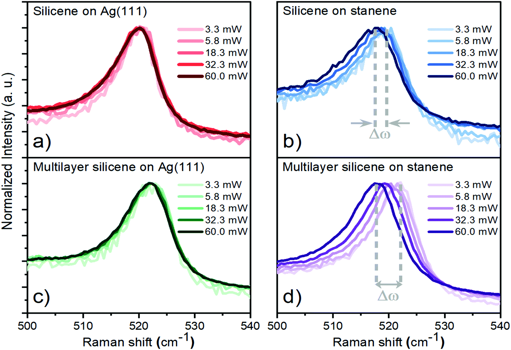 | ||
| Fig. 2 Effect of the incident laser power increase on the Raman spectra of (a) silicene, (b) silicene on stanene, (c) multilayer silicene and (d) multilayer silicene on stanene. All configurations are supported by an Ag(111) substrate. | ||
 | ||
Fig. 3 First order silicene-related Raman peak (a) position and (b) full width at half maximum versus incident laser power, extracted from two-component fit analysis of the silicene Raman spectrum. In (a) the lines result from a linear fit made on the data distribution, while in the second one they are eye guides. (c) Reflectance of bare silver (black dash), silicene on Ag(111) (red), stanene on Ag(111) (green) and silicene on stanene-Ag(111) (blue) in the spectral range from 10![[thin space (1/6-em)]](https://www.rsc.org/images/entities/char_2009.gif) 000 to 40000 cm−1. (d) Relative change of the reflectance caused by the Xene layers on the Ag(111) substrate. In (c and d) the yellow vertical line indicates the position of the laser frequency used during Raman characterization. 000 to 40000 cm−1. (d) Relative change of the reflectance caused by the Xene layers on the Ag(111) substrate. In (c and d) the yellow vertical line indicates the position of the laser frequency used during Raman characterization. | ||
The slope χ = ∂ω/∂P extracted for each of the configurations scrutinized is reported in Table 1.
| Configuration | χ (cm−1/mW) | Error (cm−1/mW) |
|---|---|---|
| Silicene | −0.009 | 0.002 |
| Multilayer silicene | −0.012 | 0.001 |
| Silicene on stanene | −0.035 | 0.003 |
| Multilayer silicene on stanene | −0.069 | 0.003 |
The modulus of the slope increases with the number of layers and is up to 6 times greater in samples where the stanene interlayer is present for the same number of silicene layers. Deviations among the power coefficient values confirm a distinct response of silicene on Ag(111) and silicene on stanene-Ag(111) to the increase in the incident laser power. Indeed, the trends observed in Fig. 3a indicate that when silicene is in direct contact with the Ag(111) substrate the power dependence of Δω is much weaker. In order to rationalize the effect just described, we also evaluated the power dependence of the FWHM of the main peak, reported in Fig. 3b. This study may help in differentiating the mechanisms at the origin of the observed redshift. As a matter of fact, the Raman FWHM in unsupported 2D materials is more influenced by anharmonic phonon interactions than by thermal expansion effects.19,20 While the incident power dependence of the FWHM is weak for all configurations, it increases for silicene on stanene-Ag(111) and shows dependence on silicene thickness. Specifically, the increase in bandwidth as a function of laser power is maximum for the single layer of silicene on stanene-Ag(111). On the other hand, the case of silicene on Ag(111) is similar to that of the multilayer heterostructure. This can be interpreted as if the increase of the thickness of silicene reduces the impact of the interface in the thermal dissipation. The shift in the Raman spectrum can be caused by the phonon–phonon anharmonic interaction, the deformation of the lattice due to the thermal energy contribution, and the effect of the mechanical strain induced by a thermal expansion coefficient mismatch between different layers.11 Therefore, considering the nearly power-independent FWHM, the variation of Δω shown in Fig. 3a can be explained in terms of mechanical strain induced by a different thermal expansion coefficient mismatch at the silicene–stanene interface compared with that of silicene–silver one.14 In particular, the latter contribution calls for a deeper understanding of the interaction between silicene and the supporting substrate. We point out that the peak located at the lowest Raman shift in the decomposition of the spectrum of silicene was excluded from the discussion due to its broad spectral width. Indeed, regarding our method of analysis, with an initial FWHM of the order of tens of cm−1, this component showed a completely negligible sensitivity to the laser-induced heating effect.
A better insight into the role of the stanene interlayer in mediating silicene–silver interactions was achieved through a comparative study of the reflectance of heterostructure building blocks. For this purpose, we set a control group consisting of bare and capped Ag(111), Al2O3 capped silicene on Ag(111) and Al2O3 capped stanene on Ag(111). This set of samples allowed us to experimentally observe the optical response of a monolayer of silicene emphasizing the effect of the Si–Ag and Si–Sn interfaces, while simultaneously overshadowing the effects due to increasing the number of silicene layers. Fig. 3c shows near-normal incidence reflectance measurements carried out in the wavenumber range of 10000–40000 cm−1 (1.25–5 eV), for bare Ag(111), silicene on Ag(111), stanene on Ag(111), and silicene on stanene-Ag(111) (see the Experimental section). Both theoretical and experimental reports have shown how the spectral range under investigation is of exceptional interest for evaluating the optical response of silicene and stanene. It is precisely between IR and UV regions that the characteristic absorptions of their band structures are placed.3,21 All the curves in Fig. 3c are dominated by the substrate response although distinctive elements can be attributed to silicene, stanene, or a combination of both as will be discussed below. The main recognizable spectral feature is related to the plasma edge near 30000 cm−1 (3.8 eV) which is, for silver, the result of a combination between the free-carrier (intraband) response and the onset of interband electronic transitions.22 To exclude the effects due to the optical properties of the Ag substrate and highlight the response attributable to the Xenes, we calculated the change of the measured reflectance between 10000 and 30000 cm−1 (1.25–3.8 eV) as:
 000 cm−1 (3.35 eV). It is worth noting that the latter spectral features can be a marker of the strong Si/Ag electronic interaction, as predicted within the density functional theory framework. Cinquanta and co-workers5 have shown that electronic transitions involving mixed Si → Ag and Ag → Si states are responsible for almost all the absorption between 24000 and 32000 cm−1 (3–4 eV). Conversely, the presence of stanene on Ag(111) (green line) strongly compensates for the silver plasma edge. The decrease of reflectance before its minimum value is less sharp and less deep than that observed for bare Ag(111) and it also results in a weak shift towards higher wavenumbers. Hence, single layer silicene and stanene yield different and opposite effects on the optical response of the system when they are deposited separately on the Ag(111) surface. The former results in a shift of the reflectance minimum from 31050 cm−1 (3.85 eV) to 30450 cm−1 (3.77 eV), whereas the latter to 32430 cm−1 (4.02 eV). It is intriguing to observe the overall result of the combined silicene and stanene layers when they are piled up in a heterostructure fashion. As pointed out above, the reflectance of the silicene–stanene heterostructure (blue curve) shows a gradual decrease, and its minimum is still shifted to a higher wavenumber as with the stanene layer. The plasma edge compensation is less steep than for a single layer of silicene or stanene. More importantly, the spectral marker at 27000 cm−1 is not present, thus confirming the role of the stanene layer in preventing the silicene/Ag electronic hybridization. As a final remark, we stress that although the tuning of the plasmonic response by changing the local dielectric environment of the metal is well known, in the present case a shift of the silver plasma edge is obtained by combining different atomically thin layers, for which the definition of the dielectric constant has been recently questioned in favor of the local polarizability of the electronic distribution.23 This scenario discloses promising opportunities to tune the plasmonic response of Ag-based nanostructures24 by stacking Xenes of different nature on top.
Conclusions
We investigated for the first time the optical response of silicene in the new context of Xene-based heterostructures. Although we carried out an indirect evaluation of the thermal response through Raman spectroscopy, our results pave the way for the validation of the thermal properties of silicene. In particular, embedding silicene (or generally, other Xenes) in the heterostructures proves to be a viable layout to target thermoelectric applications as theoretically proposed.25,26 We also establish a connection between the opto-thermal Raman responses and the optical reflectances from differently configured silicene and silicene–stanene heterostructures on silver in terms of increased optical absorption in the visible spectral range. Surprisingly, although experimental determination of the effects due to each Xene is challenging, we showed that the optical reflectance is conditioned by the details of the Xene–silver interfaces, thus providing a quick tool for ex situ identification of the heterostructure constituents. Finally, the Xene-induced shifts of the silver plasma edge open up the possibility of engineering the metal's plasmonic response by piling up Xenes of different nature on top of the Ag(111) substrate.Experimental
Xene growth
Silicene and stanene layers were grown using a Scienta Omicron LAB10 MBE system that is equipped with the low energy electron diffraction (LEED) and Auger electron spectroscopy (AES) probes for in situ characterization. As mentioned elsewhere in detail, a typical sample production scheme follows three steps: preparation, growth, and encapsulation. Several cycles of sputtering and consecutive high temperature annealing (∼550 °C) were performed on commercial Ag(111) substrates before Xene growth. For heterostructures, first a Sn layer was deposited on the prepared substrate, then the Si layer is deposited on top of tin. The multilayered silicene samples were obtained by increasing the deposition time and monitoring the thickness by means of a calibrated quartz microbalance. Before unloading, the samples were encapsulated with a non-reactive and amorphous Al2O3 capping layer to prevent degradation under ambient conditions and allow ex situ characterization.Raman spectroscopy
Raman measurements were performed using a Jobin–Yvon T6400 spectrometer in backscattering configuration with 532 nm continuous-wave excitation and a 50 × (0.75 numerical aperture) objective. To obtain the variation of Raman response versus the incident laser power we introduced a neutral density filter in the optical path and irradiated the sample surface with a series of laser power from 1.8 to 60.0 mW at room temperature. We measured the output laser power before the objective to take into account the laser energy loss in the optical path and the attenuation due to the filter. All the spectra were acquired with an exposure time of 20 seconds, considering 3 accumulations.NIR-UV spectroscopy
Additional characterization of the samples was performed using a JASCO 760v spectrometer, covering the NIR-UV spectral region from 10000 to 40000 cm−1 at room temperature. The reflectance at near-normal incidence with respect to the surface (capping layer side) was measured by taking as reference an aluminum mirror. The possibility of neglecting the encapsulating layer from the optical analysis was confirmed by comparing the reflectances of bare and capped Ag (see Fig. S5, ESI†). It is worth stressing that the high reflectivity of the silver substrate made the measurements extremely sensitive to inhomogeneities and tilts of the reflective surface. Several spectral acquisitions have therefore been necessary to control the experimental errors.
Author contributions
All the authors have given approval to the final version of the manuscript. E. Bonaventura: formal analysis, investigation, writing – original draft, and writing – review and editing. C. Martella: conceptualization, supervision, investigation, validation, writing – original draft, and writing – review and editing. D. S. Dhungana: investigation, writing – review and editing. C. Grazianetti: conceptualization, supervision, validation, writing – original draft, and writing – review and editing. S. Macis: investigation, writing – review and editing. S. Lupi: investigation, supervision, and writing – review and editing. E. Bonera: investigation, supervision, and writing – review and editing. A. Molle: conceptualization, formal analysis, supervision, investigation, validation, writing – review and editing, and funding acquisition.Conflicts of interest
There are no conflicts to declare.Acknowledgements
EU funding support from the H2020 research and innovation programme under the ERC-COG 2017 Grant no. 772261 “XFab.” is acknowledged. EB thanks the University of Milano Bicocca for funding (Bando Infrastrutture di Ricerca 2021).Notes and references
- A. Molle, J. Goldberger, M. Houssa, Y. Xu, S.-C. Zhang and D. Akinwande, Nat. Mater., 2017, 16, 163–169 CrossRef CAS PubMed.
- N. R. Glavin, R. Rao, V. Varshney, E. Bianco, A. Apte, A. Roy, E. Ringe and P. M. Ajayan, Adv. Mater., 2020, 32, 1904302 CrossRef CAS PubMed.
- L. Matthes, O. Pulci and F. Bechstedt, New J. Phys., 2014, 16, 105007 CrossRef.
- A. Molle, G. Faraone, A. Lamperti, D. Chiappe, E. Cinquanta, C. Martella, E. Bonera, E. Scalise and C. Grazianetti, Faraday Discuss., 2021, 227, 171–183 RSC.
- E. Cinquanta, G. Fratesi, S. Dal Conte, C. Grazianetti, F. Scotognella, S. Stagira, C. Vozzi, G. Onida and A. Molle, Phys. Rev. B: Condens. Matter Mater. Phys., 2015, 92, 165427 CrossRef.
- C. Hogan, O. Pulci, P. Gori, F. Bechstedt, D. S. Martin, E. E. Barritt, A. Curcella, G. Prevot and Y. Borensztein, Phys. Rev. B: Condens. Matter Mater. Phys., 2018, 97, 195407 CrossRef CAS.
- D. S. Dhungana, C. Grazianetti, C. Martella, S. Achilli, G. Fratesi and A. Molle, Adv. Funct. Mater., 2021, 31, 2102797 CrossRef CAS.
- Y. Liu, B. N. Shivananju, Y. Wang, Y. Zhang, W. Yu, S. Xiao, T. Sun, W. Ma, H. Mu, S. Lin, H. Zhang, Y. Lu, C. W. Qiu, S. Li and Q. Bao, ACS Appl. Mater. Interfaces, 2017, 9, 36137–36145 CrossRef CAS PubMed.
- E. Cinquanta, E. Scalise, D. Chiappe, C. Grazianetti, B. van den Broek, M. Houssa, M. Fanciulli and A. Molle, J. Phys. Chem. C, 2013, 117, 16719–16724 CrossRef CAS.
- C. Grazianetti, E. Cinquanta, L. Tao, P. De Padova, C. Quaresima, C. Ottaviani, D. Akinwande and A. Molle, ACS Nano, 2017, 11, 3376–3382 CrossRef CAS PubMed.
- D. Tristant, A. Cupo, X. Ling and V. Meunier, ACS Nano, 2019, 13, 10456–10468 CrossRef CAS PubMed.
- I. Calizo, S. Ghosh, W. Bao, F. Miao, C. Ning Lau and A. A. Balandin, Solid State Commun., 2009, 149, 1132–1135 CrossRef CAS.
- T. Wang, R. Wang, P. Yuan, S. Xu, J. Liu and X. Wang, Adv. Mater. Interfaces, 2017, 4, 1700233 CrossRef.
- G. Faraone, R. Sipala, M. Mariani, C. Martella, C. Grazianetti, A. Molle and E. Bonera, J. Phys. Chem. C, 2021, 125, 8711 CrossRef PubMed.
- E. Bonera and A. Molle, Nanomaterials, 2022, 12, 1410 CrossRef CAS PubMed.
- L. Zhang, Z. Lu, Y. Song, L. Zhao, B. Bhatia, K. R. Bagnall and E. N. Wang, Nano Lett., 2019, 19, 4745–4751 CrossRef CAS PubMed.
- Q. Feng, D. Wei, Y. Su, Z. Zhou, F. Wang and C. Tian, Small, 2021, 17, 2006146 CrossRef CAS PubMed.
- D. Solonenko, O. D. Gordan, G. Le Lay, H. Sahin, S. Cahangirov, D. R. T. Zahn and P. Vogt, 2D Mater., 2016, 4, 015008 CrossRef.
- A. T. Apostolov, I. N. Apostolova and J. M. Wesselinowa, J. Phys.: Condens. Matter, 2012, 24, 235401 CrossRef CAS PubMed.
- E. A. Kolesov, M. S. Tivanov, O. V. Korolik, O. O. Kapitanova, H. D. Cho, T. W. Kang and G. N. Panin, Carbon, 2019, 141, 190–197 CrossRef CAS.
- S. Saxena, R. P. Chaudhary and S. Shukla, Sci. Rep., 2016, 6, 31073 CrossRef CAS PubMed.
- P. B. Johnson and R. W. Christy, Phys. Rev. B: Solid State, 1972, 6, 4370–4379 CrossRef CAS.
- T. Tian, D. Scullion, D. Hughes, L. H. Li, C.-J. Shih, J. Coleman, M. Chhowalla and E. J. G. Santos, Nano Lett., 2019, 20, 841–851 CrossRef PubMed.
- Z. M. Abd El-Fattah, V. Mkhitaryan, J. Brede, L. Fernández, C. Li, Q. Guo, A. Ghosh, A. R. Echarri, D. Naveh, F. Xia, J. E. Ortega and F. J. García De Abajo, ACS Nano, 2019, 13, 7771–7779 CrossRef CAS PubMed.
- M. Noshin, A. I. Khan and S. Subrina, Nanotechnology, 2018, 29, 185706 CrossRef PubMed.
- B. Zhu, Q. Chen, S. Jiang, M. Holt, W. Zhu, D. Akinwande and L. Tao, InfoMat, 2021, 3, 271–292 CrossRef CAS.
Footnote |
| † Electronic supplementary information (ESI) available. See DOI: https://doi.org/10.1039/d2nh00219a |
| This journal is © The Royal Society of Chemistry 2022 |