
Novel charm of 2D materials engineering in memristor: when electronics encounter layered morphology
Saima
Batool
 ab,
Muhammad
Idrees
c,
Shi-Rui
Zhang
d,
Su-Ting
Han
e and
Ye
Zhou
*a
ab,
Muhammad
Idrees
c,
Shi-Rui
Zhang
d,
Su-Ting
Han
e and
Ye
Zhou
*a
aInstitute for Advanced Study, Shenzhen University, Shenzhen, 518060, P. R. China. E-mail: yezhou@szu.edu.cn
bKey Laboratory of Optoelectronic Devices and Systems of Ministry of Education and Guangdong Province, Institute of Microscale Optoelectronics, College of Physics and Optoelectronic Engineering, Shenzhen University, Shenzhen, 518060, P. R. China
cAdditive Manufacturing Institute, College of Mechatronics and Control Engineering, Shenzhen University, Shenzhen 518060, P. R. China
dDepartment of Electronic Materials Engineering, Research School of Physics, The Australian National University, Canberra, Australian Capital Territory 2601, Australia
eCollege of Electronics Science & Technology, Shenzhen University, Shenzhen, 518060, P. R. China
First published on 15th March 2022
Abstract
The family of two-dimensional (2D) materials composed of atomically thin layers connected via van der Waals interactions has attracted much curiosity due to a variety of intriguing physical, optical, and electrical characteristics. The significance of analyzing statistics on electrical devices and circuits based on 2D materials is seldom underestimated. Certain requirements must be met to deliver scientific knowledge that is beneficial in the field of 2D electronics: synthesis and fabrication must occur at the wafer level, variations in morphology and lattice alterations must be visible and statistically verified, and device dimensions must be appropriate. The authors discussed the most recent significant concerns of 2D materials in the provided prose and attempted to highlight the prerequisites for synthesis, yield, and mechanism behind device-to-device variability, reliability, and durability benchmarking under memristors characteristics; they also indexed some useful approaches that have already been reported to be advantageous in large-scale production. Commercial applications, on the other hand, will necessitate further effort.
 Ye Zhou | Prof. Ye Zhou is a Fellow of the Royal Society of Chemistry (FRSC) and group leader at the Institute for Advanced Study, Shenzhen University. His research interests include flexible and printed electronics, organic/inorganic semiconductors, surface and interface physics, and nano-scale devices for technological applications, such as logic circuits, data storage, photonics and sensors. |
1. Introduction
High carrier mobility, an adequate bandgap, strong light–matter interaction with a big light absorption coefficient, extremely large exciton binding energy, significant spin splitting, and polarised light emission are intriguing features of the two-dimensional (2D) materials. Using the remarkable properties of 2D layered morphology in addition to metal-oxide-based semiconductor technologies to develop enhanced solid-state electronic devices is a novel idea that could help Moore's law be extended.1,2 For future applications, researchers in the area of 2D nano- and microelectronics must meet the following criteria. All synthesis and device fabrication process must be on the wafer level, the morphology, thickness fluctuations, and lattice distortions in 2D materials should be accurately defined, and actual statistics must be provided.3 Moreover, the device size should be compact enough to meet the implementation criteria. Yield, variability (cycle to cycle and/or device-to-device), reliability, and stability must all be covered, as well as explanations of the important failure configurations of every particular device should be given.Memristors can perform neuromorphic computing to mimic the functions of the human brain. The human brain is a highly efficient and perfect information processing system, including around 1011 neurons and 1015 synapses.4 Memristors can mimic biological brain networks in operation.5 Even the most sophisticated organizations face significant challenges in nanostructured device production of 2D materials on a wide scale while implementing sustainable methods and achieving remarkable performance.6–9 North America is the most stable market for memristors. The annual global market development growth rate of memristors will be approximately 80% in 2024 and USD 13.5 billion in 2027. It all comes down to the huge investment in R&D by local market enterprises, many of which are headquartered in the United States.10
In 1971, Leon Chua realized from symmetry arguments that there should be a fourth fundamental element, which he called a memristor that could be predicted as the fourth important element in the world and resistor, capacitor, and inductor, which he named memristor (short for memory resistor).11 Later hypothetical demonstrations of the presence of tremendous energies in a memristor have been directed to their implementation in an electrical device.12 Following that, Williams and his colleagues (2008) at Hewlett-Packard Laboratories initially asserted that the performance of a memristive could be empirically achieved in a real device using the Pt/TiO2/Pt structure and presented the solid-state memristor.13 The synaptic connection determines signal transmission efficiency in biological systems from one neuron to another. It can be modified through purposeful stimuli or learning process. Neuroplasticity leads to variations in synaptic weight (pre-synaptic and post-synaptic cells), and synaptic plasticity also includes the following functions (i) short-term plasticity (STP) which has been proven to be linked to cognitive functions connected with spatiotemporal information, and (ii) long term plasticity (LTP) which on the other hand is the brain system for memory and learning. (iii) Moreover, STDP is the Hebbian theory's learning rule, which includes asymmetric and symmetric STDP demonstrating Hebbian and anti-Hebbian learning. Lu and his colleagues presented a hybrid nanostructured (metal oxide semiconductor memristor) device in 2010, a neuromorphic computing synapse. Yan and his colleagues (2019) used memristors to mimic several synaptic functions, e.g., (i) LTD, (ii) LTP, (iii) PPF, (iv) and STDP.14,15 In certain ways, memristors are making progress in the field of brain neurobionics.
There are many advanced non-volatile memories like resistive random-access memory (RRAM),3,19–21 phase-change memory (PCM),22–24 and magnetic random-access memory (MRAM).25,26 These huge and permanent data storage memories showed exceptional rewards.27–29 Among the various reference devices above, we discuss some special characteristics of memristors. Memristors can switch along with various resistance states. During resistive switching, the speeds can be on the sub nanoscale dimension with high endurance, which leads to low energy consumption.28,30 The memristor's resistive switching performance is determined by its previous resistive switching states. This property can be used in neuromorphic synaptic system applications for artificial intelligence. Furthermore, the activity of biological synapses to allow the programming of time contingent signals among neural networks is crucial for the validation of spiking neural networks intended for consistent processes.31 The synapses can be realized utilizing several designs, including the complementary metal-oxide-semiconductor transistor32 and memristors.33 Of these, memristors are considered the most promising applicants in neuromorphic engineering due to their inherent competence to recall the historical information previously sent in the form of electrical signals.
2D resources have a layered morphology, and the robust covalent bond atomic level connects the thin layers. Moreover, weak van der Waals forces are present among layers. These forces offer a perfect chance for intercalation,34 which can induce potential application in diverse technologies, as their atomic thickness might permit scaled devices.35,36 By taking appealing advantage of the above-mentioned significant characteristics of 2D materials for the progressive manufacture of solid-state electronic devices, it is a pretty good tactic that would offer us a key solution to continue Moore's law.1,37 Woong Huh and his co-workers38 have reviewed and described a variety of two-dimensional materials with various memristive resistive switching mechanisms. In the field of new materials which have been used are graphene, molybdenum disulfide (MoS2), tungsten disulfide (WS2), tantalum disulfide (TaS2), h-BN, etc. According to their properties, we classified them into three categories, metallic segment (graphene), semiconducting segment (MoTe2, WSe2, MoS2, and WS2), and insulating phase (h-BN), as shown in Fig. 1a.39,40 Architecturally, three-atom-thick layered morphological structures involving WS2, WSe2, MoS2, MoTe2, and TaS2 in these transition metal atom-like Mo, W, and Ta atoms packed between usually two chalcogen atoms of S, Se, and Te. In the interim, layered structures of one atom have hexagonal lattice plans of B–N and C–C bonds, correspondingly graphene and h-BN.41–44 2D materials can deform via in-plane elongating or bending out-of-plane. Consequently, we can consider the example of graphene being bowled into carbon nanotubes that have characteristics of 2D materials in-plane and bending moduli with well-defined stretching and bending.45,46 In the meantime, van der Waals heterostructures established by three significant materials, graphene, chalcogenides, and boron nitride, display unusual optoelectronic characteristics.47 The high-quality layered boron nitride displays the 5.97 eV bandgap, which can be used as an insulator. Fig. 1b illustrates the overall band synchronization of 3 main types of heterojunctions. Flexible devices rely primarily on Young's modulus and the splitting strain constraint of two-dimensional semiconductors. Their various architectures heavily influence 2D semiconductors' Young's modulus as well as fracture strain constrain. Single-layer graphene with planar structures produced by mechanical exfoliation is recognized as that of the best material with the greatest possible Young's modulus (Fig. 1c) and the maximum breaking strain limit due to the strong sp2 hybridization C–C covalent bonds. In recent years, wafer-scale mass production of microelectronic devices based on 2D materials has achieved significant results which overcome key challenges in materials synthesis and device fabrication.50 Transition-metal dichalcogenides (TMDs) have gained substantial curiosity as auspicious applicants for developing electronic, photonics51 and valleytronics device applications.51,52 Owing to the layered morphology, it has enormously high anisotropic electrical and ionic transport features.53–56 Additionally, these materials display polymorphs of different structural phases, which propose unique physical characteristics and are acknowledged as the hot topic of interest as a substantial evolving platform to introduce low-power and high-performance memristor devices. On the other hand, TMD-based RS layers have also been studied for memristors. Among them, Sangwan and his colleagues57 examined the defect kinetics of MoS2. Recently, Yan and his colleagues58 testified that Ti3C2Tx 2D transition metal carbide memristors were used as an RS layer for mimicking biological synapses. Simultaneously, the group promoted single-layer WS2 sheets for application in the two-terminal microelectronic device, which consumes a low power at the femtosecond level. Li and colleagues6 mainly discussed two major intrinsic memristive mechanisms: polarization switching and resistive switching. Current memristor devices can efficiently mimic biological synapses and empower the assembly of neuromorphic systems as a promising non-volatile memory storage device. Low power density and high-temperature stability significantly improve the performance of memristors. Rehman and his colleagues59 presented the device structures, conduction mechanisms, resistive switching properties, and fabrication technologies of 2D-material-based RRAMs.59 In this article, we review the performance of the 2D material in terms of various memristor engineering techniques, their physical resistive switching mechanisms, and variability. The recent challenges that 2D material-based devices are facing are discussed, and reliable strategies are presented. These materials cover a complete range of physical properties from electrochemically conductive (graphene) to semiconducting (dichalcogenides) and then highly insulator materials (hexagonal h-BN). The resistive switching mechanism should be considered on a comprehensive spatiotemporal series. It needs a thoroughly cooperative implementation of in situ techniques side by side with device demonstrations. Commonly used in situ techniques are presented in Fig. 1d, for instance, scanning tunnelling microscopy, transmission electron microscopy, optical microscopy, scanning transmission X-ray microscopy, conductive atomic force microscopy, electron beam-induced current imaging, and cyclic voltammetry.18
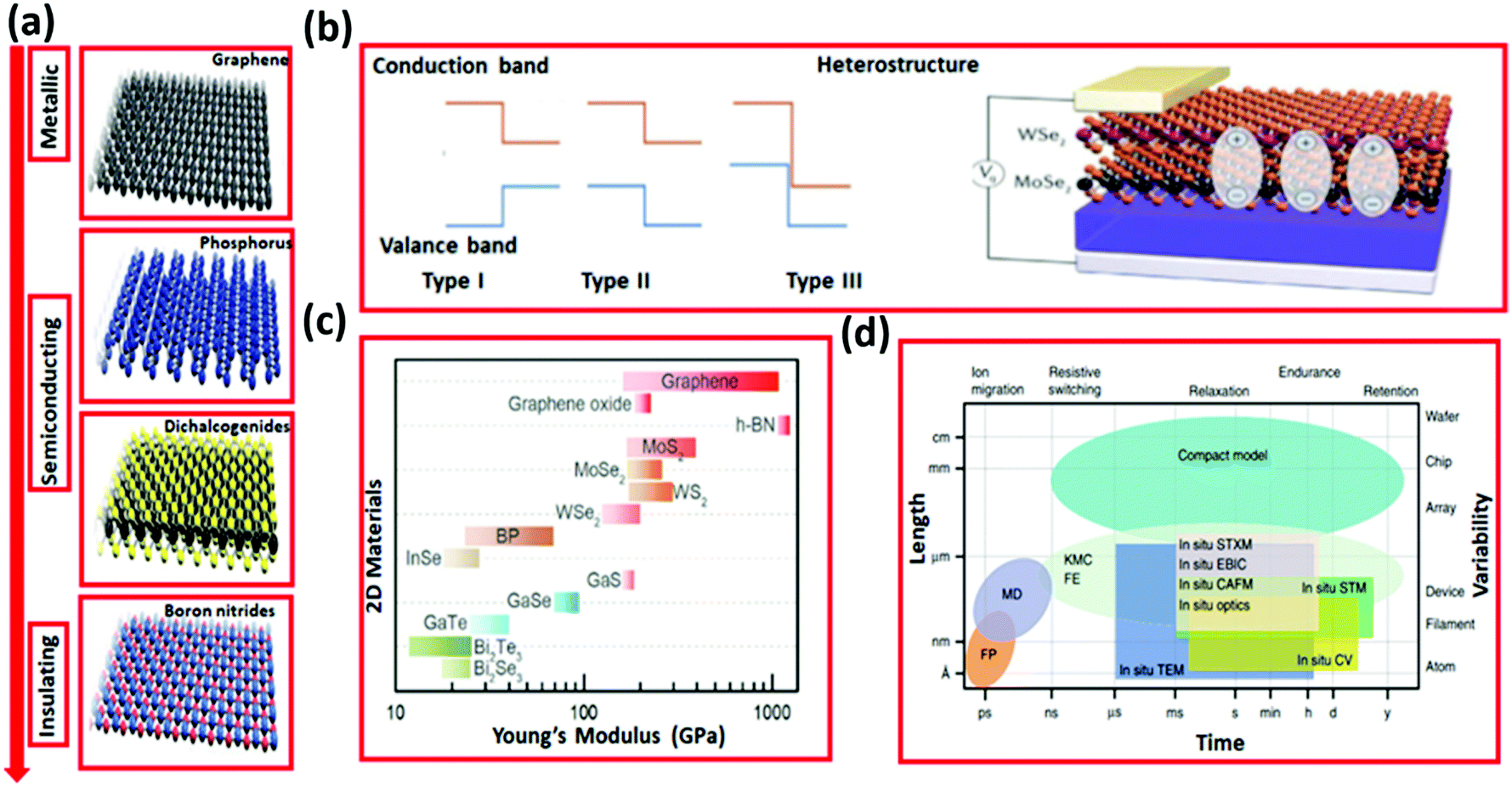 | ||
| Fig. 1 (a) 2D materials family. (b) Three different types of heterojunctions of 2D materials have different energy band arrangements. (c) Heterostructure of various material layers.16 Reproduced from ref. 16 with permission from IOPScience, copyright [2017]. (c) Young's modulus,17 reproduced from ref. 17 with permission from Wiley, copyright [2017]. (d) Spatiotemporal resolution of several in situ systems and device demonstrating methods.18 Reproduced from ref. 13 with permission from Springer Nature, copyright [2017]. | ||
In this review, we looked at memristor devices made of 2D materials in detail, which appeared among the most intriguing electronic devices in recent years. We have discussed the properties, synthesis approaches and neuromorphic functionalities observed in 2D material-based synapses and also their artificial neural applications in depth. Because of the exceptional properties, such as high carrier mobility, an adequate bandgap, and a large light absorption coefficient, these materials have been regarded as promising applicants for use in artificial synaptic devices to encourage energy-efficient neuromorphic computing. Statistical analyses on digital devices and circuits are often undervalued. The authors have addressed the most pressing integration problems which these devices encounter e.g., stressing the importance of appropriate synthesis approach, yield, variability between devices, consistency, and stability performance analysis, and laying out feasible approaches in research papers that are helpful to the industry. Nonetheless, neuromorphic applications based on 2D synaptic devices are still in their early stage. A schematic diagram of the main emphases points of this review is presented in Fig. 2.
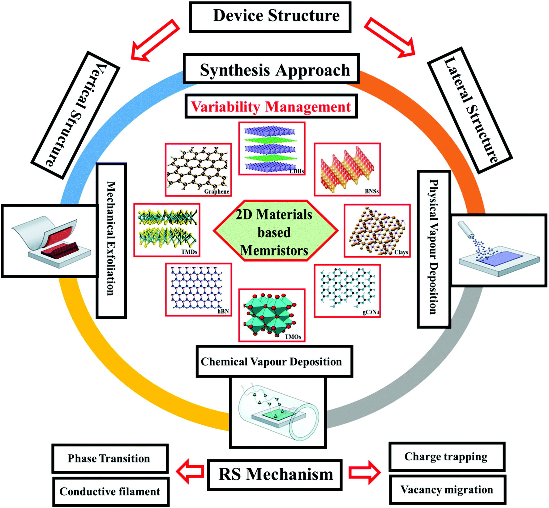 | ||
| Fig. 2 The main points of this review are depicted in a diagram, together with the various types of 2D materials, their synthesis techniques, different structures, RS mechanisms, and application in 2 terminal memristor devices.48,49 Reproduced from ref. 48 with permission from Springer Nature copyright [2017]. Reproduced from ref. 49 with permission from Elsevier, copyright [2019]. | ||
2. Synthesis strategies for 2D materials
The surface-to-volume proportion of the two-dimensional materials is high, and the bandgap is appropriate (Fig. 3a). For practical applications in semiconductor technology and optoelectronic devices, the ability to synthesize 2D materials reliably is required. There are various synthesis approaches for 2D material-based functional, active layers. They are commonly classified into the following categories: (i) top-down and (ii) bottom-up strategies (Fig. 3b). The first top-down technique includes exfoliation (Fig. 3c) (mechanical, chemical, solution-based, and liquid-phase exfoliation). The bottom-up technique includes following the synthesis process of 2D materials, chemical vapor deposition (CVD), physical vapor deposition (PVD) (Fig. 3d), pulsed laser deposition (PLD), and wet chemical methods. Two-dimensional materials are commonly made using three techniques: mechanical cleavage, physical vapor deposition (PVD), and chemical vapor deposition (CVD), as shown in Fig. 4. Micromechanical cleavage, also known as the Scotch tape approach, is being used to exfoliate single- and few-layer sheets. This approach produces crystalline samples appropriate for micrometer-scale electrical and optical devices. Researchers have selectively extracted, shaped, and stacked sheets with regulated thickness and orientation because of recent breakthroughs in exfoliation processes.77 Physical vapor deposition (PVD) is a technique for depositing a material on a substrate using a heated atomic source. In most cases, PVD requires an ultrahigh vacuum (UHV) and the very best purity atomic source materials.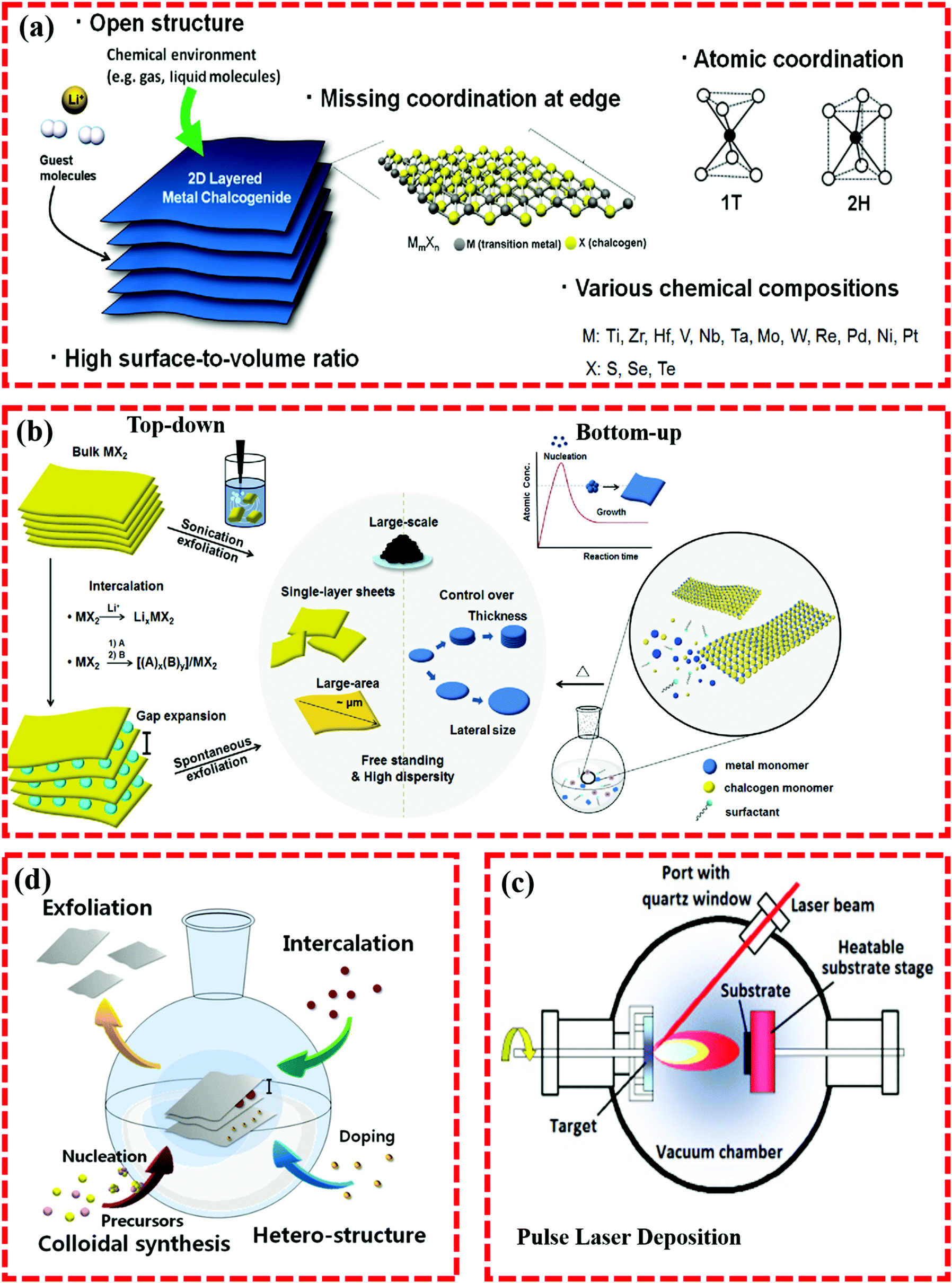 | ||
| Fig. 3 (a) 2D material properties. Within each layer of TMC nanostructures, metal and chalcogen atomic nuclei are tightly linked. (b) Top-down and bottom-up techniques to solution-based production of two-dimensional layered materials nanosheets.60 Reproduced from ref. 60 with permission from Royal Society of Chemistry, copyright [2018]. (c) Intercalation exfoliation and (d) pulse laser deposition.61 Reproduced from ref. 61 with permission from Elsevier, copyright [2019]. | ||
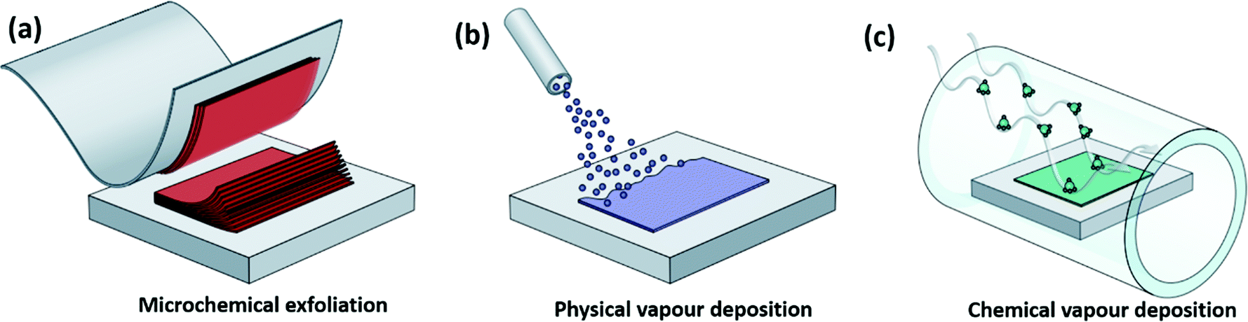 | ||
| Fig. 4 Basic 2D material synthesis techniques. Microchemical exfoliation (a), physical vapor deposition (b), and chemical vapor deposition (c).48 Reproduced from ref. 48 with permission from Springer Nature, copyright [2017]. | ||
Surface-sensitive methods can be used to study samples created under UHV conditions in situ, preserving the material's pristine state.78 CVD is a technique for growing 2D materials that involves the breakdown or reaction between gases, liquid materials, or solid species in a precise environment.79 The most effective substrates for CVD are usually those that are nucleophilic. The synthesis could be done at a variety of pressures, from barometric pressure to ultrahigh. The growth process differs depending on the substrate: at the same time as those with the poor precursor, solubility could catalyze the self-limiting production of single-crystal thin layers although others incorporate huge quantities of the precursors separate into the single-layer upon cooling. Solid-state precursors are injected further into the growing medium to achieve surface breakdown or separation. When the substrate is suitably heated to commence sublimation or diffusion operations, a surface enriched with the precursor's component develops. This layer then condenses as a 2D phase. Memristor device fabrication via a 2D material-based active layer for brain-inspired neuromorphic applications has attracted much attention.80,81 Considerable attention has been devoted to enlightening the synthesis of the active layer material in fundamental memristive devices.82,83 The stochasticity of the physical resistance switching mechanism in the devices is a key problem. This uncertainty initiates due to device-to-device variations between several devices and the cycle-to-cycle dissimilarities in single devices among various cycles.84,85
2.1. Top-down approach
The production of ultrathin nanosheets in top-down nanofabrication is accomplished by a physical or/and chemical technique. The top-down physical approach exfoliates layered van der Waals solids into single or/and few-layer materials using the mechanical strength of ultrasonic vibrational forces. On the other hand, the top-down chemical technique primarily focuses on chemical reactions triggered by electrostatic interaction, heating, as well as other means. To understand 2D materials synthesis techniques in a more convenient way a flow sheet diagram has been drawn in Fig. 5.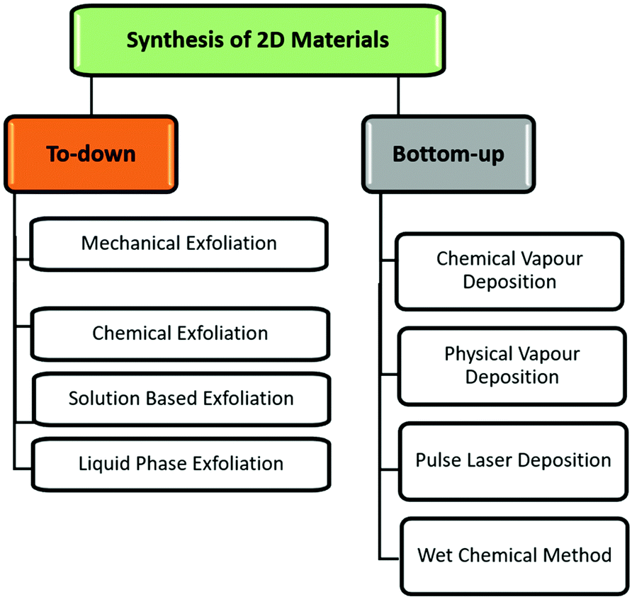 | ||
| Fig. 5 Flow sheet diagram lists the 2D material synthesis techniques. | ||
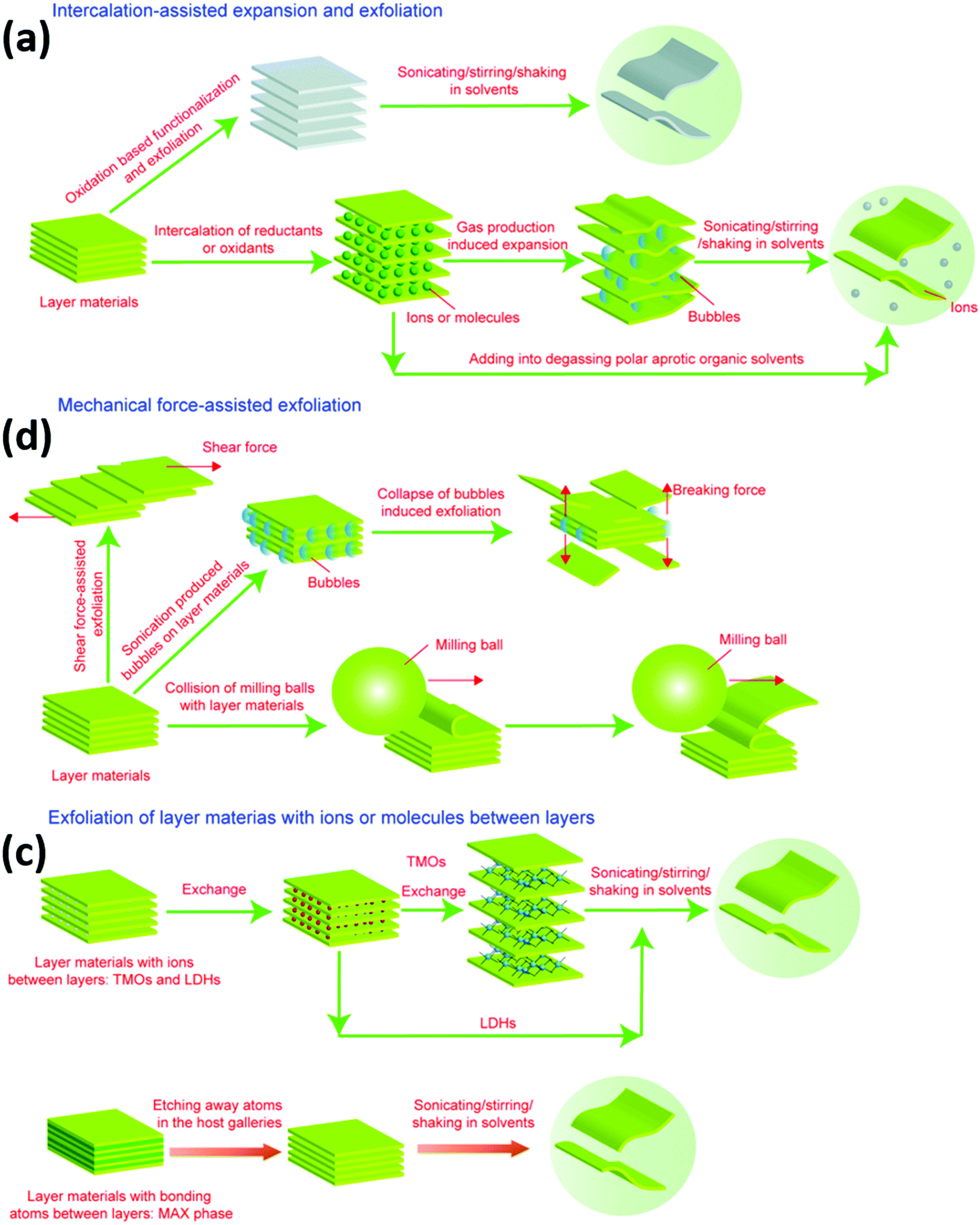 | ||
| Fig. 6 Various methods to prepare 2D material-based nanosheets via exfoliation. (a) Intercalation assisted expansion and exfoliation significantly used for graphene. (b) Exfoliation aided by mechanical force, and (c) ion/molecule exfoliation of 2D layered species.86 Reproduced from ref. 86 with permission from the Royal Society of Chemistry, copyright [2018]. | ||
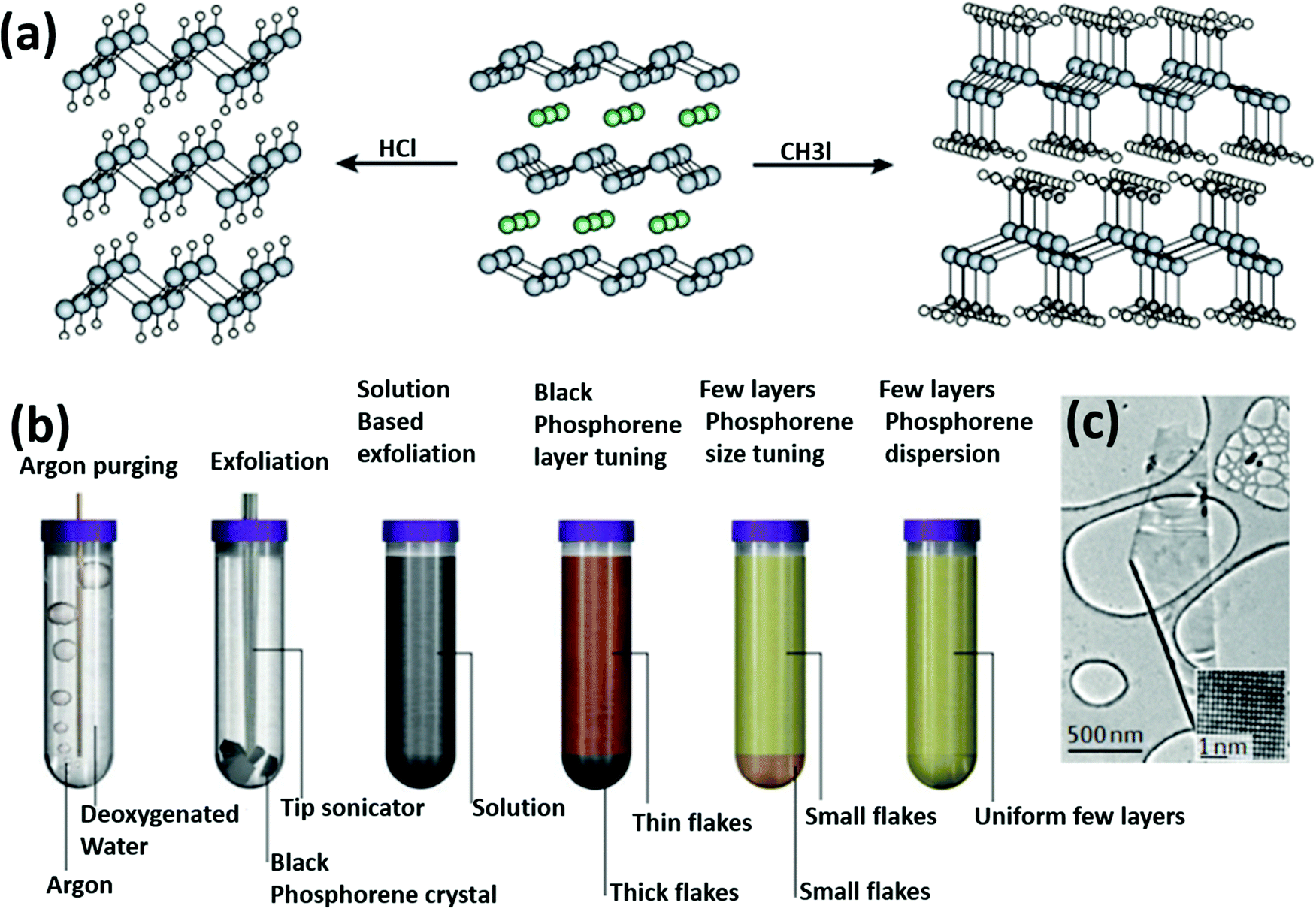
Solution Based Exfoliation (LPE), chemically processed ‘wet’ exfoliation methods offer a scalable way to separate single-crystal thin sheets with precise thickness control. On the other hand, synthetic elemental 2D materials frequently need particular preparation processes due to their instabilities in the air. Varieties of materials that do not have bulk counterparts, germanene, for example, could be recovered from bulk crystals if the structure is correct, for instance, CaGe2, which is made up of covalent bonding layers placed among layers of metal cations.97 When CaGe2 is treated with HCl (Fig. 7a), hydrogenated germanene is formed, which is stable under ambient settings. CaGe2 is treated with CH3I to produce methylated germanane Fig. 7a, which results in more stable layers.98 This functionalization improves the layers' stability and their light-emitting characteristics in the case of methylated layers. However, even though organic solvents can be used to exfoliate black phosphorus, approaches involving deoxygenated water have recently been as seen in transmission electron microscopy, and has recently been shown to produce high-quality sheets while maintaining the properties and composition of immaculate black phosphorus (Fig. 7b). Transmission electron microscopy (TEM) images presented in Fig. 7c demonstrate atomic-scale and large-scale brilliant field images of black phosphorus flakes.98,99
2.2. Bottom-up approach
For the synthesis of ultrathin and good-quality nanocomposites, we used a bottom-up approach. The materials production on the nanoscale is made possible via bottom-up processes, by using atomic or/and molecular resources. Then 2D materials could be produced with efficiency and effectiveness. The cost of large-scale production by using this approach is generally more expensive than the top-down approach.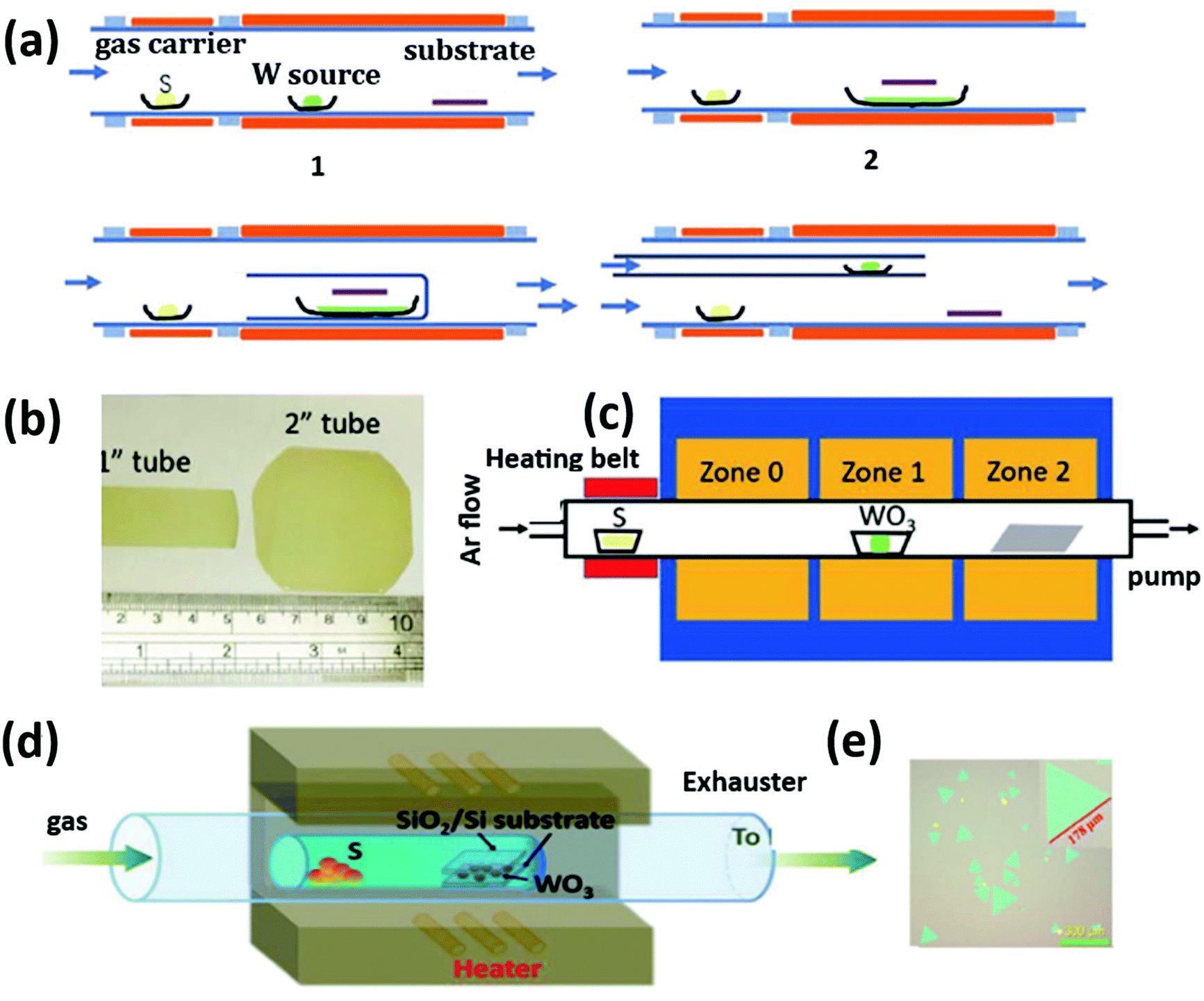 | ||
| Fig. 8 (a) A four configuration arrangement for synthesizing WS2via a CVD technique and (b) single layers of WS2 on the wafer level. (c) The multi-zone tube furnace.121 Reproduced from ref. 121 with permission from Springer, copyright [2018]. (d) WS2 monolayer synthesis. (e) WS2 optical image.122 Reproduced from ref. 122 with permission from Wiley, copyright [2016]. | ||
CVD is thought to be a useful method to grow layered materials on the surface of a metal substance. Several issues influence the resulting materials, e.g., type of precursor, the solubility percentage of the carbonaceous material of the metal component, interlayer lattice spacing fringes, crystal purity, a ratio of strain, and temperature of the whole assembly.101,102 After fine-tuning the environment of the CVD technique, we can skillfully adjust the thickness of the layers' crystal size and its purity.103 Somani and colleagues have used the thermal CVD technique and successfully designed planer structured thin graphene.104 The substrate was cost-effective (camphor on nickel) to synthesize a few graphene layers.
3. 2D materials
Two-dimensional materials make up a novel family of nanostructured materials with promising features that can be used as emerging materials for extremely thin semiconductor devices in the future.105 Meanwhile, after discovering graphene,21,106,107 various 2D materials, for instance TMDs, h-BN, and as well as black phosphorus (BP), have all been extensively investigated.108–110 The reference collection of nanostructured 2D materials, ranging from metal to insulators, provides us with a variety of options for designing diverse devices. Nowadays, 2D materials are famous for their exclusive properties, such as low dimensional assemblies and special physical and chemical characteristics.3.1. Characteristics of 2D materials
High carrier mobility, an adequate bandgap, strong light–matter interaction with a big light absorption coefficient, an extremely large exciting binding energy, significant spin splitting, and polarized light emission are all desirable features of TMDs. All of these intriguing characteristics make the 2D materials an excellent candidate for use in memristors, optical modulators, light-emitting devices, and a variety of other applications.The interlayer spacings in van der Waals materials are covalently bonded via chemical connections. Furthermore, the mobility is extremely great as it is up to 120![[thin space (1/6-em)]](https://www.rsc.org/images/entities/char_2009.gif) 000 cm2 V−1 s−1111,112 and the mobility is also high up to 1000 cm2 V−1 s−1112 for thte 10 nm thin BP film. The above factors can influence the switching speed of 2D structured memristors and regulate the on/off ratio, power consumption during RS, and operating voltage.112–114 We can synthesize 2D materials on any substrate, regardless of lattice disparity, using simple synthesis approaches such as solution-based methods, a mechanical exfoliating method which is very well-known, liquid-phase exfoliation, and also chemical vapor deposition. Furthermore, we may change the physical properties of 2D materials using various methods, such as defect induction, ion intercalation (Li-ion), and doping.115–117 Because of their atomic thickness, neuromorphic synaptic applications can benefit from them. As a result, synaptic devices made of a 2D material may respond to various stimuli, including strain field, electric field, and Joule heating. Mechanical faults, including such intrinsic defects and grain structure, have a significant impact on the intrinsic characteristics of underlying atomic layers in 2D materials.118–120 We could introduce point defects and grain boundaries using various techniques, including electron beam irradiation, changing growth conditions, and post-plasma treatment.123–125 As a result, we may change the electrochemical and photonic characteristics using the above approaches.123
000 cm2 V−1 s−1111,112 and the mobility is also high up to 1000 cm2 V−1 s−1112 for thte 10 nm thin BP film. The above factors can influence the switching speed of 2D structured memristors and regulate the on/off ratio, power consumption during RS, and operating voltage.112–114 We can synthesize 2D materials on any substrate, regardless of lattice disparity, using simple synthesis approaches such as solution-based methods, a mechanical exfoliating method which is very well-known, liquid-phase exfoliation, and also chemical vapor deposition. Furthermore, we may change the physical properties of 2D materials using various methods, such as defect induction, ion intercalation (Li-ion), and doping.115–117 Because of their atomic thickness, neuromorphic synaptic applications can benefit from them. As a result, synaptic devices made of a 2D material may respond to various stimuli, including strain field, electric field, and Joule heating. Mechanical faults, including such intrinsic defects and grain structure, have a significant impact on the intrinsic characteristics of underlying atomic layers in 2D materials.118–120 We could introduce point defects and grain boundaries using various techniques, including electron beam irradiation, changing growth conditions, and post-plasma treatment.123–125 As a result, we may change the electrochemical and photonic characteristics using the above approaches.123
Sulfur vacancies, for example, are found in layered MoS2 and act as electron contributors, allowing the identification of contributor locations on the inner side of the bandgap.126,127 These openings present potential networks for ion transport, which might assist the development of memristors and synapses. In 2D metal/h-BN/metal memristors, the boron vacancies result from the flow of boron ions in the direction of the anode, yielding a track that metal ions may fill.128,129 Hypocritical heating could insert the oxygen atoms inside MoS2 at room temperature, and layered MoS2−xOx was achieved.130 The S vacancies are molded due to the thermophoresis effect. These S positions act as pouches for the movable O ions. Finally, the oxygen ions fill and leave the new S vacancies, and this phenomenon chiefly helps to modify the resistance.130 These defects are also responsible for creating and distorting conductive filaments in several 2D-based memristors via oxidation, migration, and reduction progressions. The relocation of ions typically happens in the out of plane route with help from structural defects. For example, the defect-free single-layered MoS2 sheets need 35.01 eV of energy to transport Ag+ ions.
On the other hand, single-layered MoS2 with defects needs 1.81 eV of energy.124,131 Defects in graphene layers have similar effects, and metal ion traveling is just possible due to defects. Due to defects, the place/dimensions of conductive filaments might be precisely controlled.132,133 The 2D materials interact significantly with environmental stimuli because of their thin atomic layers and decreased screening efficiency. The polymorph property is a significant feature of TMDs.134 Commonly, TMDs have five categories of phases together with 2H, 3R 1T, 1T′, and Td stages.117 MoTe2 presented the various phase change between its monolayers of 2H and 1T′ following ionic liquid gating. On the other hand, MoS2 and MoSe2 practice the 2H phase (trigonal prismatic) to distort the 1T phase (octahedral transition) via alkali intercalation.135–139 The polymorph transition leads to the application of 2D materials as non-volatile memristor and synapse devices.3,140,141 When we consider the character of the crystalline phase of 2D materials, several crystalline phases have already been exposed e.g., α, β, γ, κ and δ phases.142,143 A single-crystal few-layered material has three phases (α, β, and γ phases) altogether steady at ambient temperature. For instance, β-In2Se3 has low resistivity with an insufficient sequence of magnitude. Still, it is also lower than other phases (α and γ), and this phase transition is irreversible. Most importantly, during SET, the β phase is at a low resistance state. During RESET, the γ phase is at a higher resistance state.29 Photoresponsivity for 2D metal chalcogenides can be from the infrared to ultraviolet range.29,146 The monolayer of TMDs such as MoS2, MoSe2, WS2, and WSe2 can grasp sunlight optical density up to 15% inside the visible light spectrum.147 Furthermore, the 2D material based on the van der Waals heterostructure can result in functional devices for enabling research in artificial intelligence.
Fig. 9a demonstrates a graphic diagram of the Pd/WS2/Pt memristor device with TEM micrographs of the WS2, which specify that the WS2 contained a layered physical morphology (Fig. 9b). The WS2 has 0.645 nm d spacing and (002) crystal orientation (Fig. 9c). The multiple dots (red and blue) presented a beautiful hexagon that specified compact hexagonal morphology, a good presentation of a 2H-WS2 unit cell.62Fig. 9d presented the schematic design of the MoS2-UCNPs film with a device structure, and Fig. 9e presents the side view through SEM. AFM images of the active layer fabricated via a spin coating technique are shown in Fig. 9f.144 Wang and his colleagues designed a robust graphene/MoS2−xOx/graphene memristor (Fig. 9g). The multilayer graphene was ∼8 nm thick, and the MoS2 has been automatically used exfoliated, and positioned at the SiO2/Si wafer substrate. The optical image of a representative GMG memristor device showed a stacked vdW heterostructure (Fig. 9h). The high angle annular dark-field (HAADF) TEM image displays layered morphology (Fig. 9i).
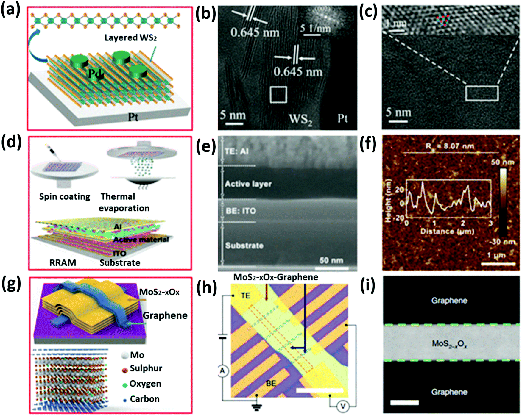 | ||
| Fig. 9 (a) Schematic diagram of the Pd/WS2/Pt memristor device, (b) TEM micrographs, and (c) HRTEM structure showing 0.654 nm surface spacing which conforms to the 002-crystal alignment.62 Reproduced from ref. 62 with permission from Wiley, copyright [2019]. (d) The schematic drawing of the MoS2-UCNPs fabrication, and the (e) SEM, and (f) AFM of the surface structure of the active layer.144 Reproduced from ref. 144 with permission from Wiley, copyright [2018]. (g and h) The schematic drawing, optical microscope image, and dimension arrangement with four-probe sizes of a GMG device and (i) the cross-section HAADF image of the MoS2−xOx upholds the layered crystal.145 Reproduced from ref. 145 with permission from Springer Nature, copyright [2018]. | ||
4. Structure and resistive switching mechanism in 2D material-based memristors
The previously reported famous two-dimensional materials and their proposed structures and resistive switching mechanism routes are summarized in Fig. 10 and 11. Various 2D materials were used as an active layer to fabricate artificial synaptic devices, the initial stage in creating a highly energy-efficient neural network model (Fig. 10a).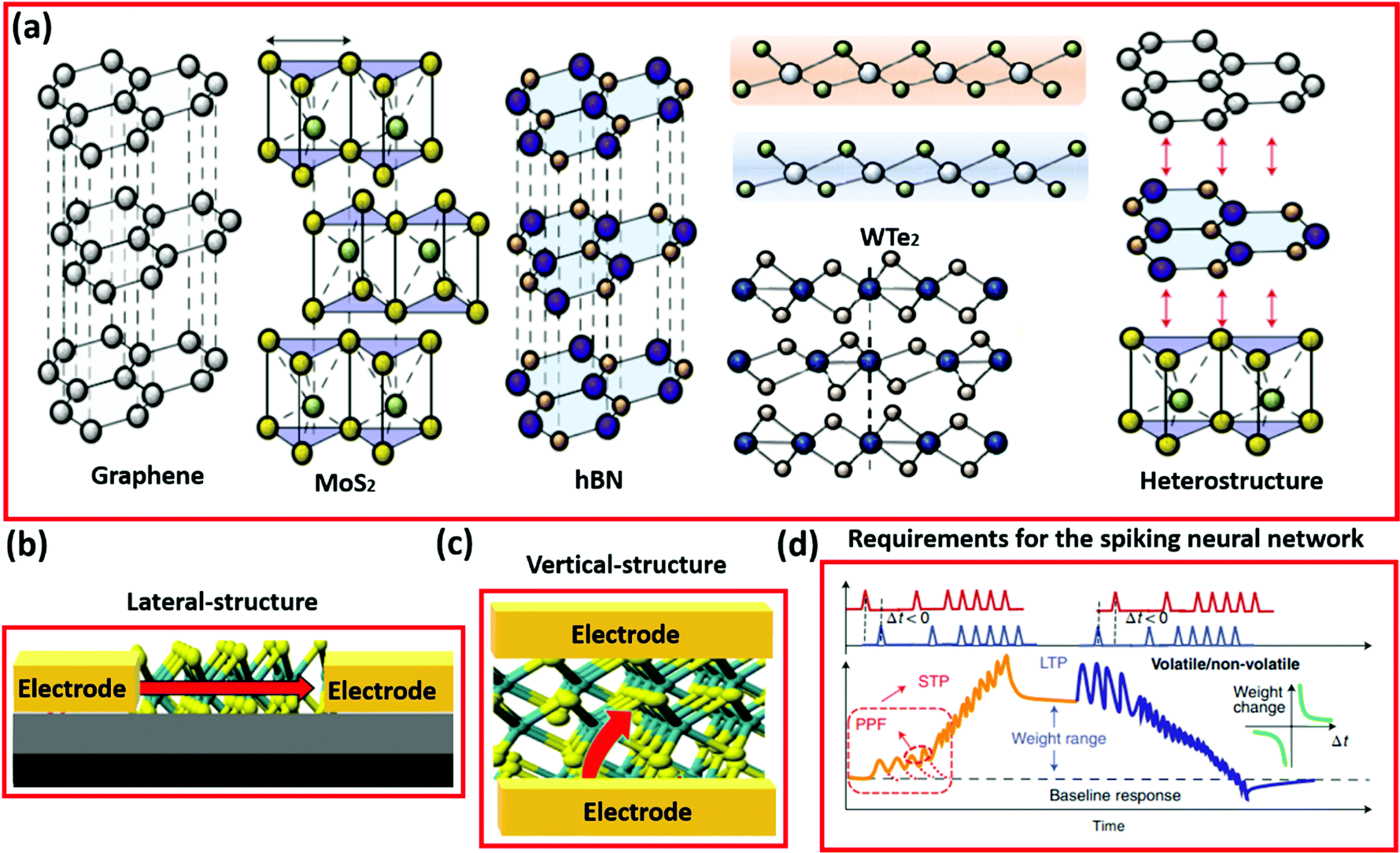 | ||
| Fig. 10 Review of the 2D material-based memristor devices with diverse materials149 and structural differences (lateral, vertical). Reproduced from ref. 149 with permission from Springer Nature, copyright [2020]. | ||
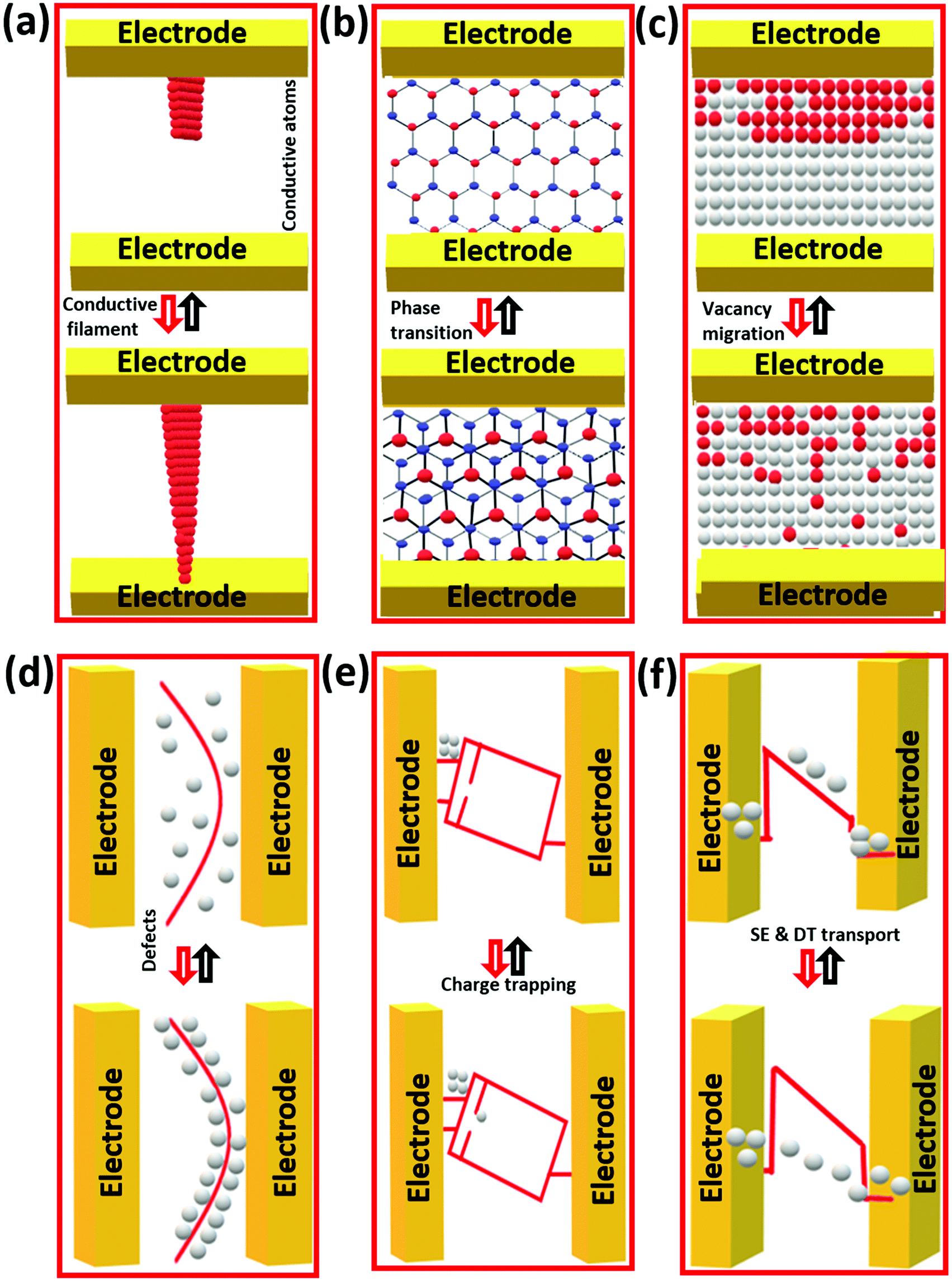 | ||
| Fig. 11 Mechanisms of resistive switching in the 2D material-based memristor devices. (a) conductive filament formation, (b) phase transition, (c) vacancy migration, (d) defects formation, (e) charge trapping and (f) Schottky emission (SE) and direct tunneling (DT). | ||
The structural geometry of 2D material-based memristor devices would be categorized into two groups entitled lateral and vertical devices (Fig. 10b and c). The working mechanism of each device depends upon the structure and active material. Zhang et al.148 discussed the fundamental mechanisms of RS behaviors in different types of 2D materials compared with solid-state memristors and also the fabrication of the device. Firstly, the electrodes of the lateral-memristor horizontally arranged on the dielectric surface are presented in Fig. 10a. The charge moves from the in orientation, and analog-like resistance changes occur as a result of defect mobility towards the grain interface or structural phase change within the 2D materials.150 The atomically thin layer is exposed in lateral devices, so it is quite easy to carry out in situ measurements. The mechanism behind resistive switching can be confirmed via in situ characterization.55,57,151 The flow of charges in memristor devices is out-of-plane in vertical-structure devices (Fig. 10c). The 2D material-based active layer is inserted along with the upper and lower electrodes.145,151–153
The resistive switching mechanisms in vertical-structure memristors148 include filament formation154 phase transition,155 vacancy migration156,157 (Fig. 11(a–c)), defects formation, and charge trapping158,159 as presented in Fig. 11(d and e). The Schottky emission (SE) and direct tunneling (DT) are also significantly mentioned in Fig. 11f.160–163 Depending on the suggested structures and materials, these devices use a variety of mechanisms. Furthermore, in situ characterizations are extremely straightforward to examine the morphology of the active layers made of 2D materials such as MoS2 and WS2 due to the nanostructured atomic layer morphology. As a result, the comparator resistive switching mechanism and various synaptic functions can be the authority to ensure those presented in Fig. 10d (including LTP, LTD, and STDP).
Table 1 classifies memristive switching mechanisms based on the active layer materials, fabrication approach, RS mechanism, electrode materials, switching voltage, ON/OFF ratio, endurance, and retention time. In particular, lateral and vertical operate at low power and have various features and functionality that assist in complex learning. Bulk materials fabricated by memristors have a high rate of reliability, stability, endurance, and retention as compared to layered materials, which can be improved by high-quality 2D materials and changing their morphology via heterostructure fabrication.
| Active layer material | Fabrication method | RS mechanism | Electrode's materials | Switching voltage | On/off ratio | Endurance | Retention time | Ref. |
|---|---|---|---|---|---|---|---|---|
| WS2 | Solution | Vacancies | Pd/Pt | 0.6 | — | 75 | 1.8 × 10⁴ | 62 |
| WSe2 | Mechanical ex-foliation | Vacancies | Ag/Graphene | 0.2–0.5 | 102 | — | — | 63 |
| ZrO2/WS2 | Large-area RF sputtering process | Filament Formation | Ag/Pt | 0.1–1.4 | 103 | 109 | — | 64 |
| WO-x/WSe2 | Vacancy Migration | Ag/Graphene | 0.2 | 107 | 103 | 103 | 63 | |
| MoS2 | LPE | ECM, CFs | Ag/Au | 3.5 | 1.6 × 10² | — | — | 65 |
| MoS2 | CVD | SE-DT | Au/Au | 1.0 | 102 | 1.5 × 10² | 106 | 66 |
| Monolayer MoS2 | CVD | Grain boundary | Au/Au | 3.5 | 103 | — | >120 | 67 |
| MoS2 nanofibers | Solution | SCLC | Rgo/rGO | — | 102 | 50 | — | 68 |
| MoOx/MoS2 | LPE | Charge trapping | Ag/Ag | 0.1–0.2 | 106 | 104 | 104 | 69 |
| MoS2 double-layer | MO CVD | ECM | Cu/Au | 0.1–0.2 | — | — | — | 70 |
| MoSe2 | Solution | Charge trapping | Au/ITO | 3.8 | 103 | — | 103 | 71 |
| MoTe2 | Mechanical exfoliation | Lattice distortion/phase transition | Ti/Ni Ti/Au | 2.3 | 102 | — | 103 | 72 |
| h-BN | CVD | Grain Boundary | Ti/Cu | 0.4 | 106 | — | 10 h | 73 |
| h-BN | CVD | ECM | ITO/Ag | 0.7 | 102 | 550 | 103 | 74 |
| h-BN-PVOH | Solution | SCLC | ITO/Ag | 0.78 | 102 | >1000 | — | 75 |
| TaS2 | Chemical vapor transport method | Phase transition | Ti/Ti | 3.0 | 103 | — | — | 76 |
Resistive switching mechanism in low dimensional systems
Several evolving memories, including magnetic memory, phase change memory, ferroelectric tunnel junctions, and resistive switching memory, have been studied in recent decades.164 Within these developing devices, memristors have several characteristics including non-volatility, small size, random data access, and are easy to fabricate with very simple structural morphology. Due to the above mentioned properties, various materials are being investigated for memristive properties. There are numerous materials which can exhibit memristive attributes. Binary oxides,165 2D materials, perovskites, bioinspired materials, polymers, halide perovskites, and low dimensional materials (nano-composites) are examples of these.166 Each kind of material seems to have economic benefits in its working principles and/or attributes, that also helps in terms of a better resistive switching device and artificial synapses performance. There are two main types of memristor working mechanisms (i) filamentary resistive switching, and (ii) interface type switching.167 As per the electrode and dielectric materials, bipolar filament resistive switching of memristor is classified as electrochemical metallization (ECM) and valence change memory (VCM).168 ECM is common in various oxides, organic materials and perovskites with electrodes of electrochemically active metals such as Ag and Cu.In most cases, the VCM mechanism is established in an active material layer and inert metal electrodes. The resistive switching layer is typically composed of a transition metal oxide, such as TiOx, HfOx, TaOx and AlOx, as well as perovskites such as BiFeO3 and SrTiO3.176,177 Here, the conductive filament is made up of ionic vacancies. To create oxygen vacancies, the electrode should act as an oxygen reservoir. A physical or chemical phenomenon at the dielectric and electrode interface causes interface type switching.178
The polymer-based active layer in the memristor device changes the conductance via various resistive switching mechanisms by modifying their intrinsic properties e.g., charge transferring, phase change, redox reactions and conformation changes. Halide perovskites have impressive on/off ratios, high switching speeds, low operation voltages, and synaptic behaviours, yet their air stabilisation needs improvement before they can be used in practical memristors and artificial synapses.
Low-dimensional materials like nanoparticles can be used in memristors. Evenly distributed Ag NPs promote Ag filament emergence while inhibiting random filament formation and rupture.179,180 Wang et al. published a paper in 2016 about TaN/Al2O3/ZnO/ITO devices with dispersed Ag NPs. In addition, MoS2 could produce ion vacancies using an oxidation process, resulting in synaptic behaviours with changes in device conductance. It has been noted that GBs in MoS2 can be easily modulated to regulate the change in resistance.
Neuromorphic functionalities observed in 2D memristive devices
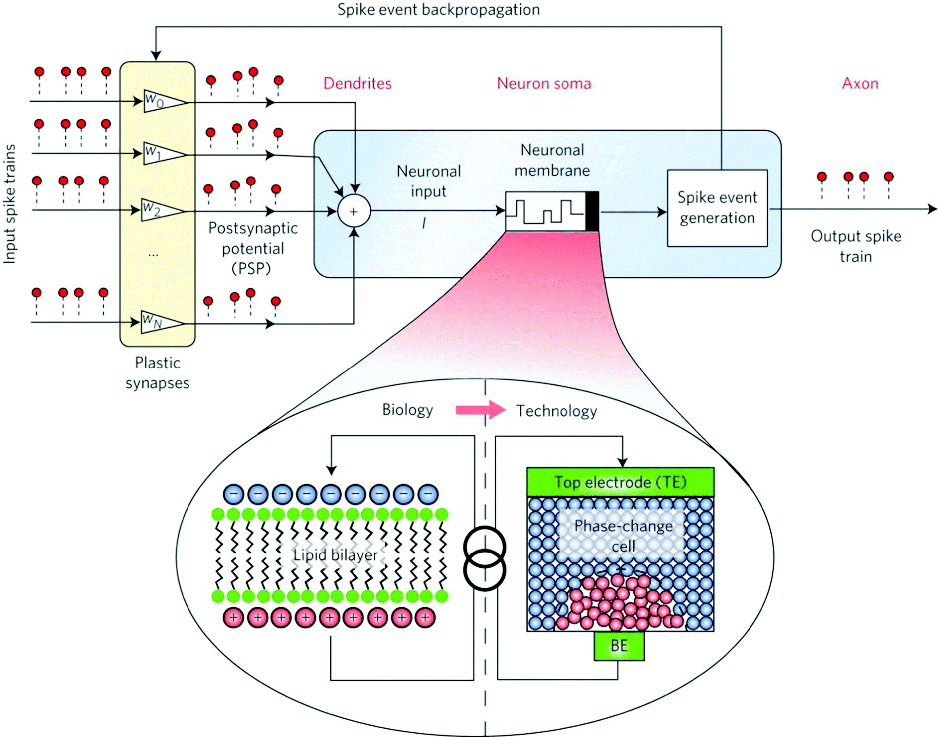
The human brain is a highly efficient and perfect information processing system, including around 1011 neurons and 1015 synapses.4 Nerve cells and synapses seem to be the brain's basic memory and cognitive units. They are also the ones that have received the most attention in neuromorphic computing systems. The synaptic connection determines the signal transmission efficiency in biological systems from one neuron to another. It is very well through purposeful stimuli or learning. Therefore, an artificial intelligence system based on neuromorphic computation offers a promising way to solve the von Neumann bottleneck.182,183 Neurons consist of somatic cells, dendrites, and axons. Generally, the amplitude of the action potential produced by a neuron is about 100 mV and the duration is 1–10 ms.184 According to the type of synapses, neural signals can be converted into chemical or electrical forms.185 Neurotransmitters are able to diffuse freely in the synaptic cleft and then integrate into receptors in the post-neuron. Two-terminal synaptic devices were studied by Strukov et al.13 based on the memristor introduced by Chua.186 In the devices, two types of configuration are often adopted: horizontal and vertical. Following that, there has been remarkable advancement in 2D material-based memristor neuromorphic devices. The ability of different 2D material candidates to mimic essential synaptic functions such as short-term plasticity (STP), long-term plasticity (LTP), short-term depression (STD), long-term depression (LTD), paired-pulse facilitation (PPF), and spike-time-dependent plasticity (STDP) learning has been studied. These functions are important for the construction of SNNs. STP, STD, LTP, and LTD are types of neuroplasticity related to short-term and long-term memory that indicate temporal or long-term enhancement/decay of synaptic connections. PPF is an example of short-term plasticity. In recent years, the memristor, a combination of memory and resistor, has emerged as one of the most essential electronic components for brain-inspired neuromorphic computing. This device can manage resistance with various states by remembering the history of past electrical stimuli, allowing it to simulate a biological synapse in the human brain's neural network. Among many candidates for memristive materials, such as metal oxides, organic materials, and low-dimensional nanomaterials, 2D layered materials have received a lot of attention owing to their excellent physical properties, electrical processability, and low-power switching capability. As a result, a great number of experimental demonstrations on 2D material-based memristors have been recorded, demonstrating their specific memristive properties and novel synaptic capabilities in comparison to classic bulk-material-based systems. This paper provides an overview of the most recent breakthroughs in the architectures, processes, and memristive properties of 2D material-based memristors. To achieve these features with low power consumption and multilevel resistance control with high reliability, a breakthrough in the discovery of new materials and the design of novel device architectures is required.5. Applications for neuromorphic computing
Artificial intelligence began as a field to replicate intelligence in a machine.188 The human brain is a highly efficient and perfect information processing system. One of the key techniques for efficiently managing data-intensive applications is brain-inspired neuromorphic computing. It is a cost-effective approach of incorporating analogue memristors into artificial neural networks or combining memristors with artificial neurons to build hardware neural networks.141 Despite the fact that such memristor-based systems give novel computer architectures, huge quantities of supplementary analogue and logic circuits are still required for the construction of artificial perceptual intelligence systems.189 Luckily, the merging of synaptic devices and biometric sensors opens up new possibilities for constructing functional neuromorphic sensory stimuli, also known as near sensor technology or edge computing.190 Current improved diagnostic strategies have demonstrated several more relevant and fascinating pieces of information about cognition inside mammals’ nervous systems, which must be precisely taken into account in solid-state devices in terms of developing quite plausible and effective human-like machines and human–machine integrations. These artificial devices could also assist scientists and therapists in mimicking and grasping various brain illnesses and problems. It would also lead to the formation of artificial sensory audio, visual, and motion systems, to investigate the progression of diseases and disorders, as well as the effects of medications, and artificially intelligent robotics which might ultimately simplify the complex surgical procedures.Yan et al.62 designed a Pd/WS2/Pt device, and the device showed the vacancy migration mechanism as presented in Fig. 11c.
The device performed admirably and consumed very little power (in the order of femtojoules). The results of trap-assisted tunnelling conduction were in accord with the fitting of the I–V curve (Fig. 12a), which determines that the defect-trap energies below the conduction band and the tunnelling distance at the HRS (LRS) are 0.62 eV (0.37 eV) and 0.94 nm (0.29 nm), respectively. Furthermore, with the 1 A program current in the ON state, it had an extremely fast ON/OFF switching times ratio (13/14 ns) as presented in Fig. 12b and c. The Pd/WS2/Pt device showed the VS and VW vacancies, and also the electron hopping effect. Fig. 12d compares the Pd/WS2/Pt device to other 2D material-based devices; obviously, this device consumes the least amount of current and power. Additionally, it effectively mimicked the significant synaptic functions including such inhibitory and excitatory under the influence of positive and negative stimulus trains. Moreover, memory and learning above the influence of PPF, STDP functions and also follow the STP transition to LTP. Significantly, it is predicted that sulfur and tungsten vacancies and electron hopping between vacancies determines the resistance switching performance. Miao and his colleagues145 fabricated a graphene/MoS2−xOx/graphene-based memristor device (Fig. 12e) that displays reproducible bipolar resistive switching with an endurance higher than or equal to 107 stable cycles with a high specific heat and a working temperature of approximately 340 °C. The in situ high-resolution transmission electron microscope (HRTEM) results at extreme temperatures indicated that the 2D material-based active layer is responsible for the devices' high thermal stability. Furthermore, in situ micrograph (STEM) investigations on a functional device revealed a heat transfer route and a resistive switching based on oxygen ion relocation. The pristine graphene/MoS2−xOx/graphene layer is shown in Fig. 12g. The on/off state of the layered atomic structure of the electrode has been discovered to be very well maintained even during long resistive switching endurance. The stability in the structure plays a significant role in establishing the device's consistency (Fig. 12h and i). Thomas Tuma et al.181 reported on a nanoscale memristive device-based biological neuron with an integrate-and-fire functionality, which could lead to significant advancements in the development of integrated circuits (Fig. 13).
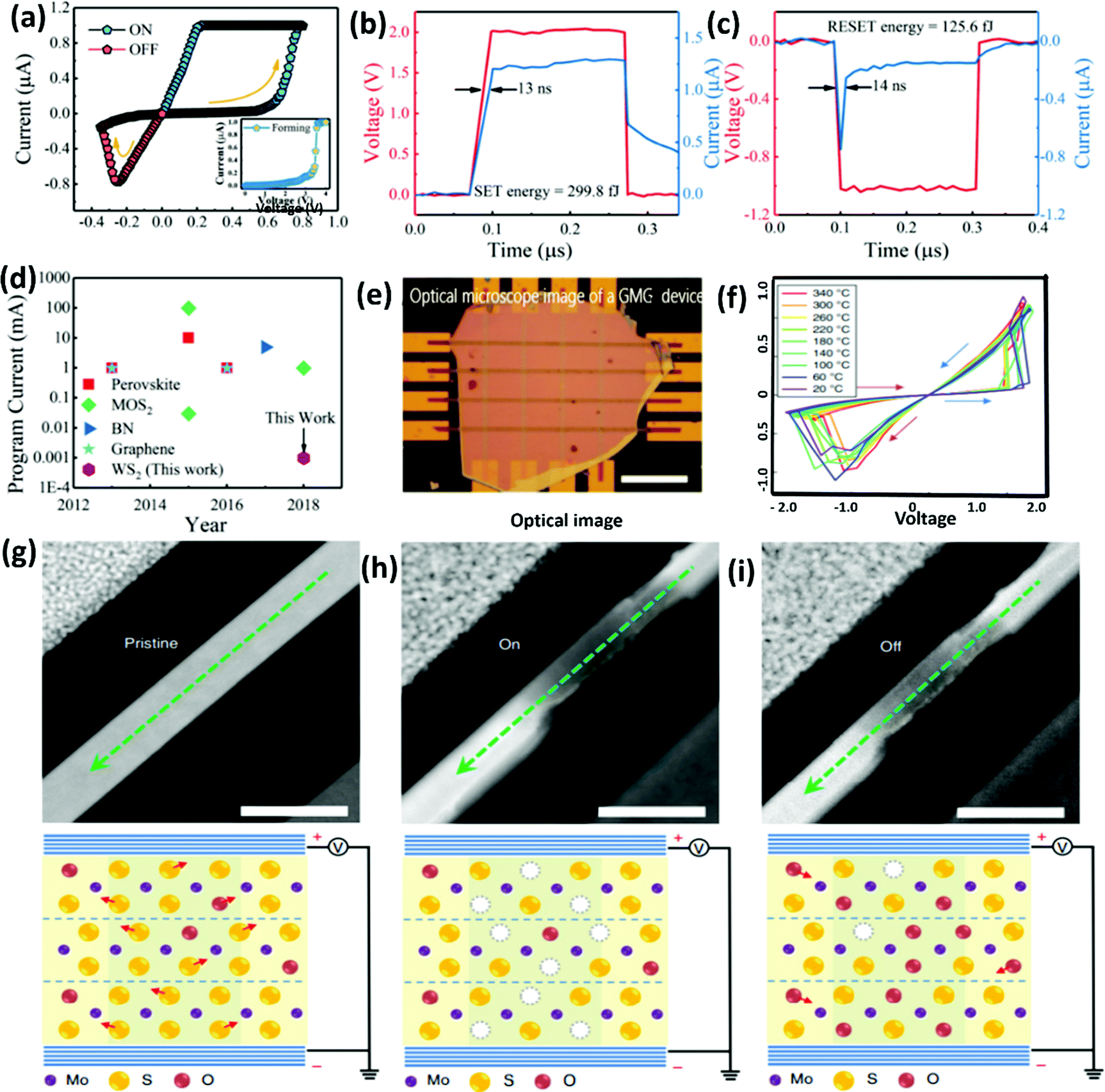 | ||
| Fig. 12 (a) Characteristic I–V arch of the Pd/WS2/Pt device. (b and c) ON/OFF states used the 13/14 ns voltage pulse,62 which was produced from ref. 62 with permission from Wiley, copyright [2018]. (d) comparison of the Pd/WS2/Pt device to other 2D material-based devices.130,169–175 (e) Graphene/MoS2−xOx/graphene optical image.145 (f) Typical I–V curve of the graphene/MoS2−xOx/graphene device. Schematic drawings of the RS mechanisms (g) pristine state, (h) ON state, and (i) OFF state. Reproduced from ref. 145 with permission from Wiley, copyright [2018]. | ||
 | ||
| Fig. 13 Artificial neuron based on a phase-change device, with an array of plastic synapses at its input.181 Reproduced from ref. 181 with permission from Springer Nature, copyright [2016]. | ||
Kumar and colleagues64 developed a ZnO/vertically aligned WS2 layer memristor (Ag/ZnO/WS2/Al) architecture (Fig. 14a) that addresses the majority of the significant difficulties in artificial synapses design to adjust the conformal development of ZnO across the WS2 layers, and cross-sectional SEM imaging was used as presented in Fig. 14b. The device demonstrates very low variability values by showing not only cycle-to-cycle stability but also device-to-device stability in performance. Temperature-dependent I–V measurements (Fig. 14c and d) and depth-dependent XPS metrics are demonstrated by the oxygen vacancies that are distributed randomly across the device. Fig. 14e depicts a typical configuration of an Ar+ sputtering and XPS measurement setup. Ar+ sputtering with a 5 keV energy was used, resulting in losing the device's layers. The XPS measurement spot diameter was set at 100 m. According to the spatial X-ray photoelectron spectroscopy (XPS), vertically oriented WS2 layers provide an excellent porous medium for the formation of defective ZnO (Fig. 14f). The generation/redistribution of oxygen vacancies was confined by a vertically aligned 2D layered design (Fig. 14g-h), ensuring high cycle-to-cycle consistency for 104 successive cycles and very low device-to-device variability. The device also meets significant requirements for neuromorphic computing, such as digital signal hysteresis loop opening (I–V characteristics), extended recognition durability, a very high current (on/off) ratio, as well as a wide range of electrical conductivity associated with various states. The Ag/ZnO/WS2/Al memristor can measure all essential properties of an artificial synapse e.g., short-to-long-term plasticity, spiking time-dependent plasticity, and also spike-timing-dependent plasticity. For read and write various dynamic functions were replicated using a memristive synapse array. This research will pave a way for developing very robust large-area neuromorphic devices with practical applications.
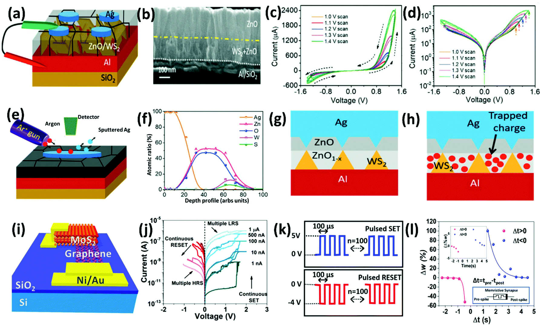 | ||
| Fig. 14 (a) The Ag/ZnO/WS2/Al memristor.64 (b) The SEM image of a memristor device demonstrated the existence of multilayers of ZnO2/WS2 and (c) I–V characteristics at various scanning rates in normal and (d) semilogarithmic scales. (e) Schematic representation of the Ar+ sputtering setup. (f) XPS measurements present the stoichiometric ZnO and WS2 layers with appropriate charge deceiving locations. (g) Without the charge trapping device structure, and (h) with the clear charge trapping location. Reproduced from ref. 64 with permission from Wiley, copyright [2019]. (i) Presents the single MoS2/graphene device, and (j) the results validate that the MoS2/graphene device demonstrates a stable change in conductance. (k) 15 pulse pulsing schematic trains, 100 identical positive/negative pulses. (l) The synaptic weight change due to pre-spike and post-spike signal timing differences.187 Reproduced from ref. 187 with permission from AIP, copyright [2019]. | ||
Krishnaprasad and his colleagues187 fabricated monolayer MoS2 based synapses via chemical vapor deposition and a graphene electrode was deposited via photolithography as presented in Fig. 14i. The non-volatile devices showed a range of conductance levels which was a function like synapses. The SET process may be achieved at varying current compliance (1 nA to 1 A) as presented in Fig. 14j. These findings show that the MoS2/graphene device exhibits a steady shift in conductance between low and high resistive switching states which is required for outdistancing synaptic potentiation and depression (Fig. 14k). They also show key synaptic features such as short-term potentiation and long-term potentiation (LTP) in the same device, and the pulse mechanism is set up in a way in which the pre-spike and post-spike transmitters just intersect once in a while for spike-timing-dependent plasticity (STDP) in Fig. 14l.
Zhu and colleagues191 fabricated Au/Ti/G/h-BN/G/Au devices (5 m × 5 m) which presented various constant resistive states at several current limits (CL) (Fig. 15a and c), which were very reliable in response to the performance. The CL was raised to control the transformation to more conductive levels while the reset voltage was used to control the transformation to less conductive levels. For high CC = 5 mA (Fig. 15c) the reset voltage was around 1 V, and for low CC = 0.5 mA it was around 3.5 V (Fig. 15a). The set voltage remained fairly constant at around 3.5 V. When utilizing CC = 1 mA (Fig. 15b) the metastable state displayed several resistive switching states (H-RS, S-LRS, and L-RS) which is presented in Fig. 15d. This operation has not been detected in graphene-free devices 5 m × 5 m (Au/Ti/h-BN/Au) or analogous devices (Au/Ti/G/h-BN/G/Au) with bigger sizes (100 m × 100 m). These findings suggest that 2D material-based memristors must be scaled up to detect an authentic device performance (e.g., tristate operation). Because graphene could indeed restrict the ionic interaction between both the metallic electrode and the h-BN resistive switching, an additional S-LRS can be formed. Variations in thermal conductivity and switching voltage have indeed been statistically examined. It has been established that all resistive states may be consistently discriminated against. This discovery is a significant step forward in creating variable memristors based on 2D layered materials and contributes to a deeper understanding of the out-of-plane RS process.
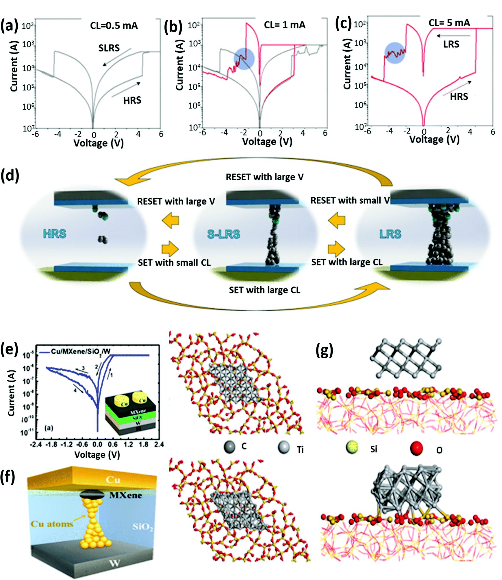 | ||
| Fig. 15 (a) In an Au/Ti/G/h-BN/G/Au device, I–V curves show two-state RS between the HRS and SLRS using CL 0.5 mA, (b) using CL 1 mA, and (c) using CL 5 mA. (d) The mechanism behind filament formation at various stages.191 Reproduced from ref. 191 with permission from the American Chemical Society, copyright [2019]. (e) Representative I–V features of the Cu/MXene/SiO2/W memristor. (f) The CFs in Cu/MXene/SiO2/W memristors are much more likely to grow in lock-step with a position of MXene, lowering the variations in the CFs. (g) DFT calculations showed unrelaxed and relaxed geometries, and the supercell of the hybrid structure of MXene (Ti3C2)/SiO2.192 Reproduced from ref. 192 with permission from AIP, copyright [2019]. | ||
Lian and his colleagues192 fabricated MXene based devices (Cu/MXene/SiO2/W) (Fig. 15e). Incorporating the desired features of silicon with that of an MXene (Ti3C2) material, a memristor-based on an MXene/SiO2 structure is fabricated. Under the same circumstances, the authors compared the performance of both devices and the Cu/Ti3C2/SiO2/W memristive devices outperform typical Cu/SiO2/W devices in switching performance. The material characterizations and DFT first-principles calculation results of the MXene/SiO2 structure presented the geometry of their structure in Fig. 15g after MXene coupling with SiO2. The findings show that conductive filaments (CFs) are much more able to constitute at the sites of MXene nanostructured materials, reducing CF variation and improving the performance of the device in Cu/MXene/SiO2/W memristors (Fig. 15f). In the meantime, the MXene/SiO2 device significantly reduces Cu ion mobility across the RS area. It increases the SiO2-based memristor performance while keeping the operating voltages low.
Arnald et al.193 used hysteresis programming in the MoS2 based device to simulate biological synapses via a solid-state device. They proved that by varying the frequency, amplitude, and polarity of gate voltage pulses, they were able to properly capture the quantal, stochastic, excitatory or inhibitory nature of neurotransmitter release in chemical synapses. They also described a potential method for replicating and engineering long-term potentiation in the human brain, which serves as the foundation for learning and memory. As shown in Fig. 16, these are structures in which the plasma membrane of the signal-carrying neuron as a presynaptic neuron is in close proximity to the plasma membrane of the target neuron as a postsynaptic neuron.
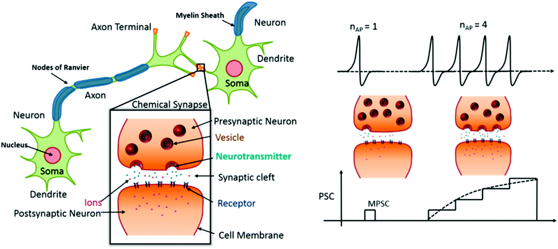 | ||
| Fig. 16 Biological synapse illustrations: the inflated assessment of a synapse with the description that the postsynaptic current expands in accordance with the presynaptic potential number.193 Reproduced with permission193 copyright 2017, American Chemical Society. | ||
The memtransistor is a multi-terminal experimental electrical component that could be used to build artificial neural networks. It's a hybrid of a memristor and a transistor. Sangwan et al.150 prepared multi-terminal memtransistors from polycrystalline monolayer MoS2. In comparison to the original brain learning behavior of long-term potentiation/depression, six-terminal MoS2 memtransistors include gate-tunable heterosynaptic capability, which two-terminal memristors do not have. Long-term potentiation and depression in MoS2 memtransistors imitated excitatory and inhibitory synapses in organisms. Farronato et al.196 presented a memtransistor device based on multilayer MoS2 with an ultrashort channel length. The device had transistor characteristics with a high resistance ratio between LRS and HRS and a memristive switching characteristic at source–drain voltages around 0.8 V. Finally, the potential of the memtransistor device was exhibited with a chain-type memory array design displaying select/unselect properties during the program and read operations. These findings pave the way for high-density, 3D memtransistor arrays based on 2D semiconductors.
Chen et al.194 developed a memory concept by designing a MoS2 quantum dot-based device, and the transmission electron microscope (TEM and STEM) images are presented in Fig. 17a and b. The device displayed nonvolatile bipolar resistive switching (on/off ratio of 104). MoS2 QD-based artificial synapse can function as a bandpass filter for low-frequency implementations. Moreover, in their MoS2 QD synapse, they illustrated short term plasticity. The charge trapping and de-trapping in quantum dots, rather than the conventional filament-based conduction in memristors, is used to achieve synaptic behaviour. The synaptic weight varied with the action potential sequence. As the number of pulses increases, Fig. 17c shows a clear increasing depression. They measured important functions of the artificial synapse including PPF and PPD (Fig. 17c). They discovered that the MoS2 QD-based synapse can function as a bandpass filter for low-frequency applications as presented in Fig. 17(d–g). MoS2 QDs have potential applications in prospective storage devices and neuromorphic technology due to their ease of fabrication and excellent memory characteristics.
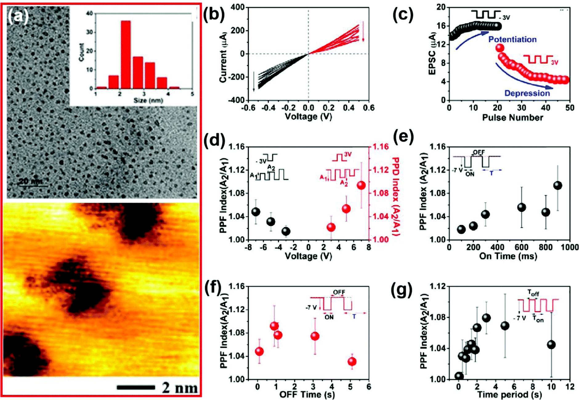 | ||
| Fig. 17 MoS2 quantum dot-based device TEM and STEM representations presented in (a) I–V characteristics, (b) Excitatory Post-Synaptic Current (EPSC), and (c) PPD and PPF variation for the amplitude of the voltage pulse. (d) Dependence of pulse time variations in PPF. (e) Dependence of time variations in PPF. (f) Dependence of time/frequency in PPF.194 Reproduced from ref. 194 with permission from Springer Nature, copyright [2020]. | ||
Conventional memristors based on bulk materials (for example, transition metal oxides) rely on top-down lithographic patterning that has limited control and tunability over neuromorphic functionality due to the strong dependence of the device response on the atomic-scale structure of defects. In contrast, emerging low dimensional nanomaterials present unprecedented control over stoichiometry, defect engineering and interfacial chemistry, which underlie synaptic behaviour. Low-dimensional nanomaterials also possess quantum phase transitions, new state variables, electrostatic tunability and atomic-level control for reconfigurable switches and neuromorphic functions. Within this class of materials, 2D nanomaterials provide an open architecture for multiple electrodes, in situ probing, and spatiotemporal responses, while zero-dimensional (0D) and one-dimensional (1D) nanomaterials enable highly sensitive covalent functionalization and redox chemistry for multi-bit states. Promising results are also emerging from hybrid systems that integrate nanomaterials of different dimensionalities. Due to their mechanical flexibility, low-dimensional nanomaterials are also facilitating the development of wearable neuromorphic applications such as afferent nerves and smart prosthetics. Here, we review recent progress in the emerging field of neuromorphic nanoelectronic materials with a focus on how the properties of 0D, 1D and 2D nanomaterials and their van der Waals heterostructures enable unique neuromorphic responses compared to inorganic and organic materials. Some important properties of 0D, 1D and 2D materials have been presented in Table 2.
| Materials | Morphology | Characteristics | Synthesis approaches | Improvements | Shortcomings |
|---|---|---|---|---|---|
| 0D | Nanoparticle | Charge trapping | Spin-coating | Easy fabrication of large-area devices | Aggregation |
| Size controllable | Light responsible | Blending | High surface to volume ratio | Temperature susceptible | |
| Self-assembled QD-based film | Light responsible flexibility | Langmuir–Blodgett electro deposition | Better solubility | Spatial uniform challenge | |
| Transparency | Better amenability to hybridize with other nanomaterials | ||||
| Piezoelectricity | Easy to be doped and functionalized | ||||
| 1D | Nanowire | Directivity | Spin-coating | Easy to form a network | Difficult to fabricate |
| Nano-rod | Light responsible flexibility | Spraying | High carrier transport | High cost | |
| Nano-fiber | Transparency | Molding | Directivity | Low surface to volume ratio | |
| Complex network | Piezoelectricity | Electro-spinning | Tuning electronic properties through p–n junction | ||
| 2D | Nano-sheet | High carrier transport | Mechanical exfoliation | Low roughness | Difficult to fabricate |
| Uniform crystallinity | Chemical exfoliation | High temperature tolerance | Specific modifications required | ||
| Ultrathin | Solution based exfoliation | High carrier transport | |||
| Light responsible | Chemical vapour deposition | ||||
| Flexibility | Physical vapour deposition | ||||
| Transparency |
6. Variability, reliability, and stability
The significance of statistical analysis on electrical devices and circuits is frequently underestimated, especially for two-dimensional materials. Previous studies have highlighted the most significant integration difficulties for such devices and emphasized the precondition to evaluate variability.197 Device-to-device variability can be defined as a deviation from the principal parameters and statistics of the devices (such as switching voltages, high and low resistance states in memristors, carrier ion mobility, leakage current, threshold voltage, and swing for FET).Several elements directly impact the yield and device-to-device variability of these devices. Device-to-device variability in 2D materials is connected with the insertion of various sorts and quantities of defects throughout the device fabrication process, material synthesis, materials transfer procedure, aging, modeling stages, and the deposit of additional coupling of diverse materials.198 Material defects have a varied effect on the variability of current flow via 2D materials in memristors. In such vertical devices, RS is a random process that still happens at the potentially weak position of an active device component when subjected to an electric current. The most common intrinsic defects in 2D material-based devices are vacancies, cracks, wrinkles, strain or stressed bonding, impurities, and, most important, variations in the thickness of a 2D material. While the most frequently identified defects are related to shifting interactions with the atmosphere in changeable bonding and interaction to adjoining components.201,202 When the defect is minor, it can influence the device's properties, increasing the (device-to-device) variability yet keeping it under an appropriate working range. Pan and colleagues created an h-BN-based memristor employing a variety of electrode materials. They concluded that inserting metal cations into the 2D materials (h-BN) layers aided the RS and that B vacancies may improve. They devised the following ways to tailor the attributes of the devices and address the issue of device-to-device variability: (i) manipulating thickness, (ii) modifying the density of grain boundaries using a doped substrate approach and (iii) interfacial electrodes, which are composed of graphene are inserted. Therefore, the storage cells exhibited free restive switching, with a low set and reset voltage ratio (0.4 and 0.8 V, respectively) and a very high ON/OFF current ratio of up to six times greater with more than ten hours of capacity retention and also negligible (device-to-device) variability.172
Villena and colleagues203 measured the variability of a metal/h-BN/metal memristor produced on various substrates (e.g., Pt, Cu, and Fe) by studying their electrical properties and resistive switching. They have utilized the CVD synthesis approach and formed 5-layer h-BN and >10-layer h-BN materials. This work focused on the problem of RS variability of device performance.204 Au/Ti/h-BN/Pt devices have been tested with identical Pt grain. These two devices had an extremely low level of variability. On the other hand, the electrical response of these two devices was different when constructed from different Pt grains. This fluctuation in electrical response was caused by differences in h-BN layers thickness on one Pt grain to the next, as shown. Whenever a comparable experiment was carried out on Cu grain-based (Au/Ti/h-BN/Cu) devices, the measured parameters revealed significantly reduced variability in six Au/Ti/h-BN/Cu devices, with low variability for (both set and reset) processes. The variability of iron-based (Au/Ag/h-BN/Fe) memristors has also been examined by applying a blend of experimental and simulation methods. Several RS cycles were performed on an Au/Ag/h-BN/Fe device (Fig. 18a). Fig. 18b demonstrates the probability distribution and cumulative probability of V SET and V RESET. When the Au/Ag/h-BN/Fe memristor data is compared to Au/Ti/h-BN/Cu memristor data, it can be shown that Au/Ag/h-BN/Fe devices have a somewhat larger variability. The calculations match well with the experimentally observed I–V sweepings in both RS (high and low), as illustrated in Fig. 18d and e. This consistency between experimental and simulation-based results shows that the h-BN stack has many conductive filaments. According to the calculations, quantum conduction (as predicted by QPC theory) is insignificant in this scenario, effective for high electrically conductive filaments. This finding supports the concept of the penetration of metallic ions from electrodes into h-BN to create the conductive filaments by confirming the Ohmic conduction of the conductive filaments. Inside the reduced voltage domain (about 0.6 V of L-RS), Fig. 14f shows Au/Ag/h-BN/Fe memristors (150 I–V curves).
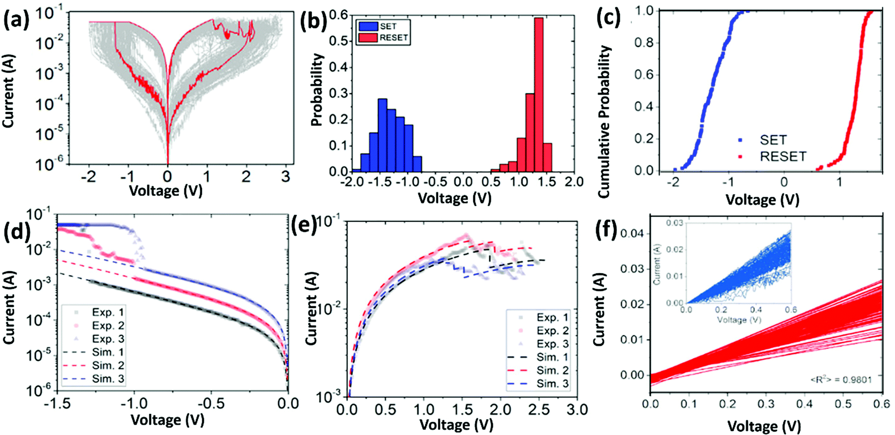 | ||
| Fig. 18 (a) The red curve presented as the first cycle about 150 sweeps of the Au/Ag/h-BN/Fe device, the set/reset voltages statistical analysis presented in (b and c). (d and e) I–V sweeps under HRS and LRS. (f) The I–V curves in the 0 V–0.6 V voltage range in the Au/Ag/h-BN/Fe device for linear regression fitting.195 Reproduced from ref. 195 with permission from Elsevier, copyright [2019]. | ||
Chen and colleagues199 fabricated an Au/h-BN/Au memristor device through the chemical vapor deposition process and realized its application as an artificial neural network aimed at image recognition. The bipolar RS characteristics were dominated in the fabricated devices as presented in Fig. 19, demonstrating 98% yield, 1.53% cyclic variability, and 5.74% device variability. The stochastic filamentary RS of one device is credited to the cycle-to-cycle variability. 1500 cycle to cycle statistical analyses for 48 memristor devices is shown in Fig. 19a. The set and reset voltage variability through the coefficient of variation (CV) was counted Fig. 19b. The lack of homogeneity in the device causes device-to-device variability, e.g., area, creases, and width variations of the active layer during assembling.205,206 The lowest variability of cycles during set and reset was 2.02%, and the maximum was 9.61%. On the other hand, the variability value among devices (device to device) increased from 6.06% to 29.07% for 48 memristor devices. For CC = 1 μA, the V-SET and RESET values decreased to 1.53% and 6.21%, respectively, for cycle-to-cycle variability. Increasing the distribution of VSET and reset VREST for 16 samples at 1 mA CC (Fig. 19c). Guo and colleagues200 claimed the fabrication and testing of 80 Ag/SnOx/SnSe memristor devices using an extremely consistent fabrication approach, with 100% yield, small set variability, and reset voltages shown in Fig. 19d.
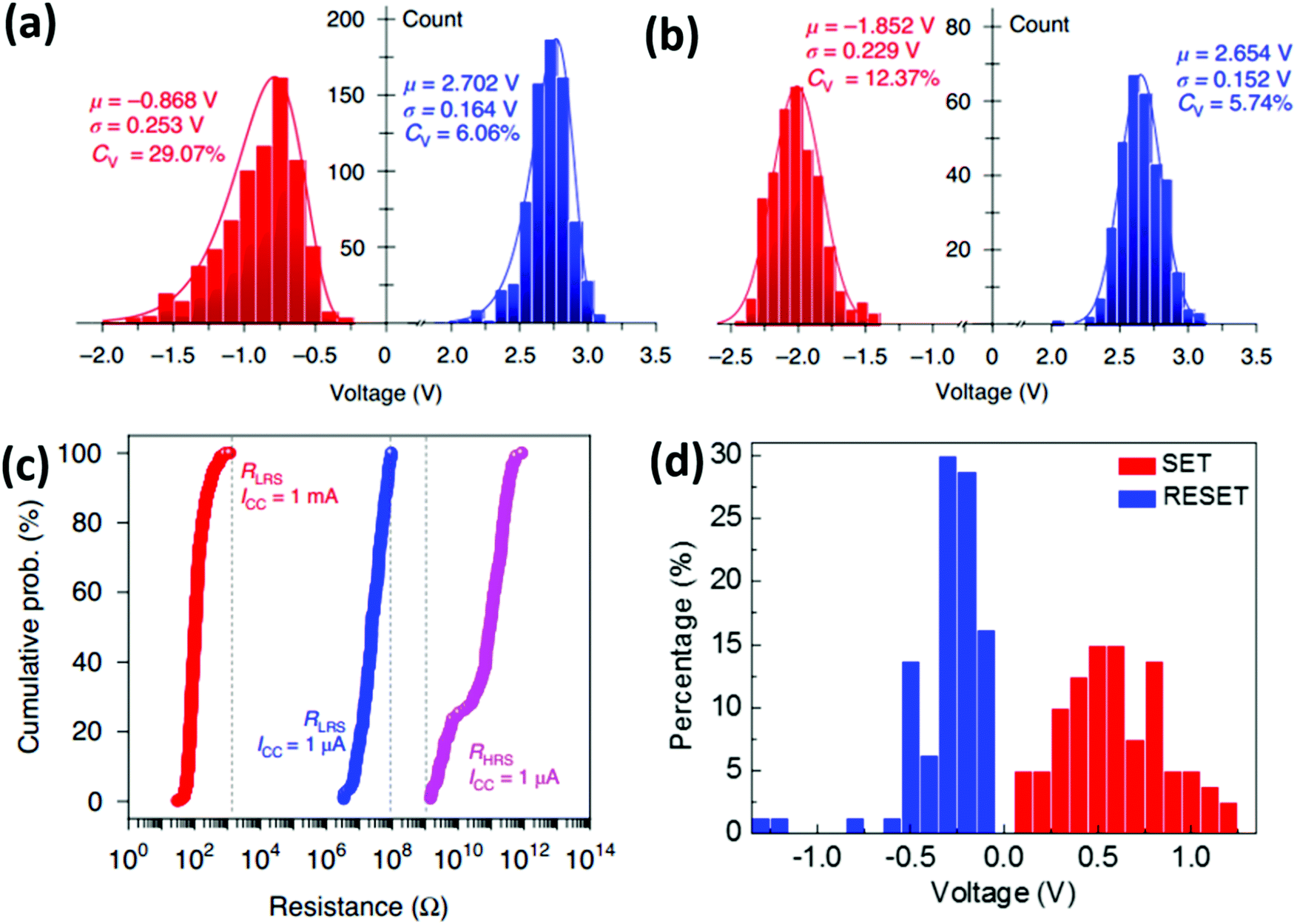 | ||
| Fig. 19 (a) Au/h-BN/Au memristive Cumulative distribution plot for 48 memristors (1500 cycles). (b) Increasing dispersal of device VSET and reset VREST for 48 samples at 1 mA. (c) Increasing distribution of VSET and reset VREST for 16 samples at 1 mA CC.199 Reproduced from ref. 199 with permission from Springer Nature, copyright [2020]. (d) Ag/SnOx/SnSe memristor statistical operation voltage of 80 as-fabricated devices.200 Reproduced from ref. 200 with permission from Elsevier, copyright [2020]. | ||
7. Challenges, possible approaches, and attitudes for 2D materials
Primarily, large-scale engineering of 2D material-based nanostructured memristor devices using low-cost approaches while achieving excellent results would be a significant challenge for the most mature businesses. Nonetheless, synthesis on a wafer scale with precise thickness is significant. With various CVD techniques, substantial surface area monolayer 2D material (such as WS2 and MoS2) films may be easily produced. However, the quality of these CVD-produced 2D material sheets is insufficient for industrial use. It is desirable to have wafer-scale single-layer 2D materials combined from huge single domain flakes with an aligned orientation. As a result, a thorough understanding of 2D materials growth behaviors is critical, especially if a severe layer-by-layer growth strategy with a high single-crystal domain size is to be developed. Immediately, a comprehensive assessment of critical structural characteristics and wafer-scale manufacturing techniques will be conducted.Second, in an open environment, the reaction between a 2D material and a substrate material generates redox reactions and the formation of new materials, affecting the original characteristics of the materials. Consistency, variability, and stability are the most common issues. Memristors are non-volatile memory storage devices, and memristor devices employed as electric synapses must show altered gigabytes. What is the correct parameter for evaluating the high yield, consistency, variability, and stability of memristor devices that may not be evident. In general, there are a few easy rules to follow: (i) instead of a single device, statistical evidence concerning several important limits and statistics of performance (figure of merit) define the consistency among a number of the devices.; (ii) statistical data about numerous significant limits and figures of merit defining the consistency of the devices. To minimize scientific swings that go unreported in hypothetical papers, the importance of statistical studies must be addressed in a thorough way on 2D material-based devices. (iii) The effective contact between metal electrodes and material films has not been fully established, despite the need for dependable electrical contact in all device applications. To date, various contact methods for decreasing the contact resistance between metal electrodes and 2D material-based channels have been investigated. Device contact that is dependable and Ohmic contact are difficult to create. It is critical to provide a versatile and universal electrical contact design. Furthermore, despite the high light–matter interaction of 2D materials, light absorption is unavoidably poor due to their atomic thickness, limiting their photodetection effectiveness. Plasmonic and photonic structures can increase the device's light absorption and, therefore, its photodetection performance, leading to functional optoelectronic memristors and synapses.
8. Summary and outlook
The characteristics of the 2D material, its production, and applications in various types of memristors for neuromorphic applications are described in this review article. The performance of the memristor is primarily concerned when a specific active layer made of 2D materials is utilized. The switching voltage, ON/OFF current ratio during RS, cycle to cycle, and device to device variability, retention time, power consumption, and other properties of memristors should be considered carefully. It is concluded that we need to boost this to meet the authentic storage requirements significantly. As a result, to satisfy current requirements, we must concentrate our efforts on the synthetic approach for 2D materials and large-area integration. During the literate review, we have gone through several synthesis strategies for 2D material-based active layers. Various synthesis techniques for 2D material-based functionals and active layers include mechanical exfoliation, liquid-phase exfoliation, and CVD. The CVD can be used to make high-quality and single-sheet films, and this is an area of study that will be pursued in the future.Second, understanding the operating process of the memristor's switching mechanism is critical to the research field. The structural characteristics of 2D materials have been addressed. According to the physical shape of the device, 2D materials offer an effective resistive switching mechanism (lateral or vertical). Typical switching processes are defect migration, phase transition, vacancy migration, filament creation, charge trapping, atomic vacancy, and trapping and de-trapping of electronic species. When a conductive filament develops inside a memristor device, it may be identified with atomic resolution under various switching conditions using an in situ probing approach and electron energy-loss spectroscopy with high 3-D resolution. A three-dimensional description of a conductive filament provides comprehensive information on its shape. The creation and extinction of conductive filaments should ideally be done at the atomic level. Aberration-corrected high-resolution TEM would be useful to detect the produced grain boundary structure. TEM can also be used to characterize atomic vacancy defects.
Third, a pioneering research topic is the 2D material-based memristor device, which is designed to store and supply data in the form of visual and electric signals. Several hybrid heterostructures have been developed to increase the number of data storage levels and improve the device's functionality. As a result, light can be introduced to switch the memristor device to determine the effectiveness of light sensitivity on performance. The optical and electrical characteristics of 2D materials can be affected by both infrared and ultraviolet light.148
In summary, we concluded our understanding in this review that even for the most advanced companies fabricating 2D material-based nanosized devices at the wafer-level by utilizing scalable methods for accomplishing outstanding performance is a considerable challenge. When we compared device fabrication with the exfoliation approach, all of the mentioned performance metrics for device fabrication via synthetic approaches are still severely hampered. While research on mechanically exfoliated layered materials may be useful as a comparison to evaluate material performance, statistical analyses into the implementations of two-dimensional layered materials-based microelectronic devices are urgently needed. It is important to keep in mind that the variables and metrics of each device's merit are decided by its practical applications in the industry. For instance, the FET device used during logic gates must operate and encounter reliability criteria different from those used to control the power flow along with a memristor device. Correspondingly, memristors for use as non-volatile memory and memristors as electronic synaptic devices perform differently. In other words, while the literature contains extensive guidance on how to evaluate the synthesis, yield, fabrication, variability, and stability, we need to adopt the following basic criteria: (i) an appropriate synthesis approach, (ii) careful fabrication and characterization should be on multiple devices, (iii) offering statistical data including all metrics and figures of merit that impact the device's reliability, and (iv) moreover, instead of relying exclusively on intuition focused schematics, analyze and evaluate failures depending on nanometric accuracy and experimental measurements. To allow a technological change, the significance of statistics on two-dimensional devices must be emphasized on a larger scale, even though crucial technical challenges risk being neglected in scholarly papers.
Conflicts of interest
There are no conflicts to declare.Acknowledgements
This work was supported by the National Natural Science Foundation of China (Grant No. 61974093), the Science and Technology Innovation Commission of Shenzhen (Grant No. RCYX20200714114524157, JCYJ20180507182042530 and JCYJ20180507182000722), and the NTUT-SZU Joint Research Program.Notes and references
- L. M. Yang, S. K. Su, H. P. Wong and L. J. Li, Nature, 2019, 567, 169–170 CrossRef PubMed.
- D. Akinwande, C. Huyghebaert, C. H. Wang, M. I. Serna, S. Goossens, L. J. Li, H. S. Wong and F. H. Koppens, Nature, 2019, 573, 507–518 CrossRef CAS PubMed.
- Q. Zhao, Z. Xie, Y.-P. Peng, K. Wang, H. Wang, X. Li, H. Wang, J. Chen, H. Zhang and X. Yan, Mater. Horiz., 2020, 7, 1495–1518 RSC.
- K. Wang, J. Chen and X. Yan, Nano Energy, 2021, 79, 105453 CrossRef CAS.
- G. Ding, Y. Wang, G. Zhang, K. Zhou, K. Zeng, Z. Li, Y. Zhou, C. Zhang, X. Chen and S. T. Han, Adv. Funct. Mater., 2019, 29, 1806637 CrossRef.
- H. Li, L. Tao and J.-B. Xu, J. Appl. Phys., 2021, 129, 050902 CrossRef CAS.
- Z. Wang, S. Joshi, S. Savelev, W. Song, R. Midya, Y. Li, M. Rao, P. Yan, S. Asapu and Y. J. Zhuo, Nat. Mater., 2018, 1, 137–145 Search PubMed.
- R. Wang, J.-Q. Yang, J.-Y. Mao, Z.-P. Wang, S. Wu, M. Zhou, T. Chen, Y. Zhou and S.-T. Han, Adv. Intell. Syst., 2020, 2, 2000055 CrossRef.
- Z. Wang, S. Joshi, S. E. Savelev, H. Jiang, R. Midya, P. Lin, M. Hu, N. Ge, J. P. Strachan and Z. J. Li, Nat. Mater., 2017, 16, 101–108 CrossRef CAS PubMed.
- A. I. Vlasov, I. V. Gudoshnikov, V. P. Zhalnin, A. T. Kadyr and V. A. Shakhnov, Entrepreneurship Sustainability Issues, 2020, 8, 98 CrossRef.
- K. Sun, J. Chen and X. J. A. F. M. Yan, Adv. Funct. Mater., 2020, 8, 2006773 Search PubMed.
- L. Liu, C. Bing, B. Gao, F. Zhang, Y. Chen, X. Liu, W. Yi, R. Han and J. Kang, Appl. Phys. A, 2011, 102, 991–996 CrossRef CAS.
- D. B. Strukov, G. S. Snider, D. R. Stewart and W. J. Duncan, Nature, 2009, 459, 1154 CrossRef CAS.
- X. Yan, Y. Pei, H. Chen, J. Zhao, Z. Zhou, H. Wang, L. Zhang, J. Wang, X. Li and C. J. Qin, Adv. Funct. Mater., 2019, 31, 18052841–18052849 Search PubMed.
- Y. Zhan, Y. Chen, Q. Zhang, J. Zhuang, M. Tian, H. Chen, L. Zhang, H. Zhang, J. He and W. Wang, Nat. Chem. Biol., 2012, 8, 897–904 CrossRef CAS PubMed.
- U. Wurstbauer, B. Miller and E. Parzinger, J. Phys. D: Appl. Phys., 2017, 17, 173001 CrossRef.
- J. Du, H. Yu, B. Liu, M. Hong, Q. Liao, Z. Zhang and Y. J. Zhang, Small Methods, 2021, 5, 2000919 CrossRef CAS PubMed.
- W. Sun, B. Gao, M. Chi, Q. Xia, J. J. Yang, H. Qian and H. J. Wu, Nat. Commun., 2019, 10, 1–13 CrossRef PubMed.
- Y. Yang, G. Yuan, Z. Yan and W. Xubing, Adv. Mater., 2017, 26, 1700425 CrossRef PubMed.
- J. Lindner, D. Burgler and S. J. Springer, Magnat. Nanostruct. Nanostruct., 2013, 44, 1–35 Search PubMed.
- K. S. Novoselov, A. K. Geim, S. V. Morozov, D. Jiang, M. I. Katsnelson, I. Grigorieva, S. Dubonos and A. J. Firsov, Nature, 2005, 438, 197–200 CrossRef CAS PubMed.
- H. Hamann, M. O. Boyle, Y. Martin, M. Rooks and M. Wickramasinghe, Nat. Mater., 2006, 5, 383–387 CrossRef CAS PubMed.
- S. B. Furber, D. R. Lester, L. A. Plana, J. D. Garside, E. Painkras, S. Temple and A. D. Brown, IEEE Trans. Comput., 2012, 62, 2454–2467 Search PubMed.
- E. M. Vinod, K. Ramesh, R. Ganesan and K. S. Sangunni, Appl. Phys. Lett., 2014, 104, 383 CrossRef.
- J. H. Chang, H. H. Chen and C. R. J. Chang, J. Phys. D: Appl. Phys., 2012, 46, 035002 CrossRef.
- C. A. Downing, A. R. Pearce, R. J. Churchill and M. E. Portnoi, Phys. Rev. B, 2015, 92, 165401 CrossRef.
- H. M. Vo, S. N. Truong, S. Shin and K. S. Min, J. IKEEE, 2014, 18, 228–233 CrossRef.
- T. W. H. Oates and S. J. Noda, Appl. Phys. Lett., 2009, 94, 053106 CrossRef.
- M. J. Hollander, Y. Liu, W.-J. Lu, L.-J. Li, Y.-P. Sun, J. A. Robinson and S. J. Datta, ACS Nano Lett., 2015, 15, 1861–1866 CrossRef CAS PubMed.
- A. C. Torrezan, J. P. Strachan, G. Medeiros-Ribeiro and R. S. J. N. Williams, Nanotechnology, 2011, 22, 485203 CrossRef PubMed.
- Y. Zhao, L. Chai, X. Yan, W. Huang, T. Fan, O. A. Al-Hartomy, A. Al-Ghamdi, S. Wageh, A. G. Al-Sehemi, Z. Xie and H. Zhang, Mater. Chem. Front., 2022 10.1039/D1QM01342D.
- J. Mcmanus, T. Ito, V. Ferreira, T. Baumgartner, J. Mey, T. Weber, J. Crusius, C. Tems, W. Berelson and R. J. Thunell, Science, 2014, 345, 665–668 CrossRef PubMed.
- M. J. Lee, B. L. Chang, D. Lee, S. R. Lee, C. Man, H. H. Ji, Y. B. Kim, C. J. Kim, D. H. Seo and S. J. Seo, Nat. Mater., 2011, 10, 625–630 CrossRef CAS PubMed.
- R. Chen, T. Zhao, W. Wu, F. Wu, L. Li, J. Qian, R. Xu, H. Wu, H. M. Albishri and A. Al-Bogami, Nano Lett., 2014, 14, 5899–5904 CrossRef CAS PubMed.
- A. D. Franklin, Science, 2015, 349, 2750 CrossRef PubMed.
- T. Skotnicki, J. A. Hutchby, T.-J. King, H.-S. Wong and F. Boeuf, IEEE Circ. Devices Mag., 2005, 21, 16–26 CrossRef.
- D. Akinwande, C. Huyghebaert, C.-H. Wang, M. I. Serna, S. Goossens, L.-J. Li, H.-S. P. Wong and F. H. Koppens, Nature, 2019, 573, 507–518 CrossRef CAS PubMed.
- W. Huh, D. Lee and C. H. Lee, Adv. Mater., 2020, 51, 2002092 CrossRef PubMed.
- M. Chhowalla, H. S. Shin, G. Eda, L.-J. Li, K. P. Loh and H. Zhang, Nat. Chem., 2013, 5, 263–275 CrossRef PubMed.
- N. Smith, S. Kevan and F. Disalvo, J. Phys. C: Solid State Phys., 1985, 18, 3175 CrossRef CAS.
- K. S. Novoselov, A. K. Geim, S. V. Morozov, D. Jiang, Y. Zhang, S. V. Dubonos, I. V. Grigorieva and A. A. Firsov, Science, 2004, 306, 666–669 CrossRef CAS PubMed.
- K. S. Novoselov, A. K. Geim, S. V. Morozov, D. Jiang, M. I. Katsnelson, I. Grigorieva, S. Dubonos and A. A. Firsov, Nature, 2005, 438, 197–200 CrossRef CAS PubMed.
- K. S. Novoselov, D. Jiang, F. Schedin, T. Booth, V. Khotkevich, S. Morozov and A. K. Geim, Proc. Natl. Acad. Sci. U. S. A., 2005, 102, 10451–10453 CrossRef CAS PubMed.
- C. R. Dean, A. F. Young, I. Meric, C. Lee, L. Wang, S. Sorgenfrei, K. Watanabe, T. Taniguchi, P. Kim and K. L. Shepard, Nat. Nanotechnol., 2010, 5, 722–726 CrossRef CAS PubMed.
- Q. Lu and R. Huang, Int. J. Appl. Mech., 2009, 1, 443–467 CrossRef.
- Q. Lu, M. Arroyo and R. Huang, J. Phys. D: Appl. Phys., 2009, 42, 102002 CrossRef.
- T. J. Ko, H. Li, S. A. Mofid, C. Yoo, E. O. ue, S. S. Han, M. S. Shawkat, A. Krishnaprasad, M. M. Islam and D. Dev, Science, 2020, 11, 101676 Search PubMed.
- A. J. Mannix, B. Kiraly, M. C. Hersam and N. P. Guisinger, Nat. Rev. Chem., 2017, 1, 1–14 CrossRef.
- T. Hu, X. Mei, Y. Wang, X. Weng and M. J. S. B. Wei, Sci. Bull., 2019, 64, 1707–1727 CrossRef CAS.
- M. Lanza, Q. Smets, C. Huyghebaert and L. J. Li, Nat. Commun., 2020, 11, 1–5 CrossRef PubMed.
- M.-J. Lee, C. B. Lee, D. Lee, S. R. Lee, M. Chang, J. H. Hur, Y.-B. Kim, C.-J. Kim, D. H. Seo and S. Seo, Nat. Mater., 2011, 10, 625–630 CrossRef CAS PubMed.
- K. F. Mak and J. Shan, Nat. Photonics, 2016, 10, 216–226 CrossRef CAS.
- J. Hong, K. Li, C. Jin, X. Zhang, Z. Zhang and J. Yuan, Phys. Rev. B, 2016, 93, 075440 CrossRef.
- C. Gong, Y. Zhang, W. Chen, J. Chu, T. Lei, J. Pu, L. Dai, C. Wu, Y. Cheng and T. Zhai, Adv. Sci., 2017, 4, 1700231 CrossRef PubMed.
- X. Zhu, D. Li, X. Liang and W. D. Lu, Nat. Mater., 2019, 18, 141–148 CrossRef CAS PubMed.
- N. L. Rodenhouse, W. H. Lowe, R. L. Gebauer, K. P. McFarland and M. S. Bank, Sci. Total Environ., 2019, 665, 1125–1134 CrossRef CAS PubMed.
- V. K. Sangwan, H.-S. Lee, H. Bergeron, I. Balla, M. E. Beck, K.-S. Chen and M. C. Hersam, Nature, 2018, 554, 500–504 CrossRef CAS PubMed.
- X. Yan, K. Wang, J. Zhao, Z. Zhou, H. Wang, J. Wang, L. Zhang, X. Li, Z. Xiao and Q. Zhao, Small, 2019, 15, 1900107 CrossRef PubMed.
- M. M. Rehman, J. Z. Gul, H. M. M. U. Rehman, W. Y. Kim and N. J. S. Ahmed, Sci. Technol. Adv. Mater., 2020, 21, 147–186 CrossRef CAS PubMed.
- J. H. Han, M. Kwak, Y. Kim and J. J. C. R. Cheon, Chem. Rev., 2018, 118, 6151–6188 CrossRef CAS PubMed.
- M. Bellardita, A. Di Paola, S. Yurdakal and L. Palmisano, Heterogen. Photocatal., 2019, 1, 25–56 Search PubMed.
- X. Yan, Q. Zhao, A. P. Chen, J. Zhao, Z. Zhou, J. Wang, H. Wang, L. Zhang, X. Li and Z. J. Xiao, Small, 2019, 15, 1901423 CrossRef PubMed.
- W. Huh, S. Jang, J. Y. Lee, D. Lee, D. Lee, J. M. Lee, H. G. Park, J. C. Kim, H. Y. Jeong and G. J. A. M. Wang, Adv. Mater., 2018, 30, 1801447 CrossRef PubMed.
- M. Kumar, D. K. Ban, S. M. Kim, J. Kim and C. P. Wong, Adv. Electron. Mater., 2019, 5, 1900467 CrossRef CAS.
- J. J. Liu, Z. Zeng, X. Cao, G. Lu, L. H. Wang, Q. L. Fan, W. Huang and H. Zhang, Small, 2012, 8, 3517–3522 CrossRef CAS PubMed.
- R. Ge, X. Wu, M. Kim, J. Shi, S. Sonde, L. Tao, Y. Zhang, J. C. Lee and D. Akinwande, ACS Nano Lett., 2018, 18, 434–441 CrossRef CAS PubMed.
- M. D. Pickett, J. Borghetti, J. J. Yang, G. Medeiros-Ribeiro and R. S. Williams, Adv. Mater., 2011, 23, 1730–1733 CrossRef CAS PubMed.
- X. Zhang, H. Xie, Z. Liu, C. Tan, Z. Luo, H. Li, J. Lin, L. Sun, W. Chen and Z. J. Xu, Angew. Chem., Int. Ed., 2015, 54, 3653–3657 CrossRef CAS PubMed.
- Q. A. Vu, Y. S. Shin, Y. R. Kim, V. L. Nguyen, W. T. Kang, H. Kim, D. H. Luong, I. M. Lee, K. Lee and D.-S. Ko, Nat. Commun., 2016, 7, 1–8 Search PubMed.
- R. Xu, H. Jang, M.-H. Lee, D. Amanov, Y. Cho, H. Kim, S. Park, H.-J. Shin and D. J. Ham, ACS Nano Lett., 2019, 19, 2411–2417 CrossRef CAS PubMed.
- X. Zhang, Z. Lai, Z. Liu, C. Tan, Y. Huang, B. Li, M. Zhao, L. Xie, W. Huang and H. J. Zhang, Angew. Chem., Int. Ed., 2015, 54, 5425–5428 CrossRef CAS PubMed.
- F. Zhang, H. Zhang, S. Krylyuk, C. A. Milligan, Y. Zhu, D. Y. Zemlyanov, L. A. Bendersky, B. P. Burton, A. V. Davydov and J. Appenzeller, Nat. Mater., 2019, 18, 55–61 CrossRef CAS PubMed.
- L. Valentini, M. Cardinali, E. Fortunati and J. Kenny, Appl. Phys. Lett., 2014, 105, 153111 CrossRef.
- C. R. Dean, A. F. Young, I. Meric, C. Lee, L. Wang, S. Sorgenfrei, K. Watanabe, T. Taniguchi, P. Kim and K. L. Shepard, Nat. Nanotechnol., 2010, 5, 722–726 CrossRef CAS PubMed.
- M. Kim, R. Ge, X. Wu, X. Lan, J. Tice, J. C. Lee and D. J. Akinwande, Nat. Commun., 2018, 9, 1–7 CrossRef PubMed.
- M. Yoshida, R. Suzuki, Y. Zhang, M. Nakano and Y. Iwasa, Sci. Adv., 2015, 1, 1500606 CrossRef PubMed.
- Y. Liu, N. O. Weiss, X. Duan, H.-C. Cheng, Y. Huang and X. J. Duan, Nat. Rev., 2016, 1, 1–17 Search PubMed.
- A. J. Rockett, Mater. Sci. Semicond., 2008, 1, 505–572 Search PubMed.
- J.-H. Lee, E. K. Lee, W.-J. Joo, Y. Jang, B.-S. Kim, J. Y. Lim, S.-H. Choi, S. J. Ahn, J. R. Ahn and M.-H. J. S. Park, Science, 2014, 344, 286–289 CrossRef CAS PubMed.
- J. J. Yang, M. D. Pickett, X. Li, D. A. Ohlberg, D. R. Stewart and R. S. Williams, Nat. Nanotechnol., 2008, 3, 429–433 CrossRef CAS PubMed.
- S. Bhattacharjee, R. Wigchering, H. G. Manning, J. J. Boland and P. K. J. Hurley, Sci. Rep., 2020, 10, 1–8 CrossRef PubMed.
- R. J. Van, M. M. Masis and E. Miranda, Quantum Point Contact Conduct., 2016, 22, 197–224 Search PubMed.
- M. Zidan, H. Omran, R. Naous, A. Sultan, H. Fahmy, W. Lu and K. Salama, Sci. Rep., 2016, 1, 1–9 Search PubMed.
- F. Alibart, L. Gao, B. D. Hoskins and D. B. Strukov, Nanaotechnology, 2012, 23, 075201 CrossRef PubMed.
- S. Choi, P. Sheridan and W. D. Lu, Sci. Rep., 2015, 5, 1–10 Search PubMed.
- X. Cai, Y. Luo, B. Liu and H.-M. J. C. S. R. Cheng, Chem. Soc. Rev., 2018, 47, 6224–6266 RSC.
- Y. Wang, Y. Zhao, X. Ding and L. Qiao, J. Energy Chem., 2021, 60, 451–479 CrossRef.
- F. Wang, Z. Wang, T. A. Shifa, Y. Wen, F. Wang, X. Zhan, Q. Wang, K. Xu, Y. Huang and L. J. Yin, Adv. Funct. Mater., 2017, 19, 1603254 CrossRef.
- F. Schedin, A. K. Geim, S. V. Morozov, E. Hill, P. Blake, M. Katsnelson and K. S. Novoselov, Nat. Mater., 2007, 6, 652–655 CrossRef CAS PubMed.
- M. Yi and Z. Shen, J. Mater. Chem. A, 2015, 3, 11700–11715 RSC.
- H. Li, J. Wu, Z. Yin and H. J. Zhang, Acc. Chem. Res., 2014, 47, 1067–1075 CrossRef CAS PubMed.
- G. S. Shmavonyan, G. Sevoyan and V. J. Aroutiounian, Armenian J. Phys., 2013, 6, 1–6 CAS.
- Y. Peng, Z. Wang and K. J. L. Zou, Langmuir, 2015, 31, 7782–7791 CrossRef CAS PubMed.
- Y. Zhang, J. P. Small, W. Pontius and P. Kim, Appl. Phys. Lett., 2005, 86, 073104 CrossRef.
- Y. Hernandez, V. Nicolosi, M. Lotya, F. M. Blighe, Z. Sun, S. De, I. McGovern, B. Holland, M. Byrne and Y. K. Gun'Ko, Nat. Nanotechnol., 2008, 3, 563–568 CrossRef CAS PubMed.
- J. N. Coleman, M. Lotya, A. O’Neill, S. D. Bergin, P. J. King, U. Khan, K. Young, A. Gaucher, S. De and R. J. Smith, Science, 2011, 331, 568–571 CrossRef CAS PubMed.
- S. Jiang, M. Q. Arguilla, N. D. Cultrara and J. E. Goldberger, Acc. Chem. Res., 2015, 48, 144–151 CrossRef CAS PubMed.
- S. Jiang, S. Butler, E. Bianco, O. D. Restrepo, W. Windl and J. E. Goldberger, Nat. Commun., 2014, 5, 1–6 Search PubMed.
- X. Ling, H. Wang, S. Huang, F. Xia and M. S. Dresselhaus, Proc. Natl. Acad. Sci. U. S. A., 2015, 112, 4523–4530 CrossRef CAS PubMed.
- X. Li, W. Cai, J. An, S. Kim, J. Nah, D. Yang, R. Piner, A. Velamakanni, I. Jung and E. J. Tutuc, Science, 2009, 324, 1312–1314 CrossRef CAS PubMed.
- O. Penkov, H.-J. Kim, H.-J. Kim and D.-E. Kim, Int. J. Precis. Eng. Manuf., 2014, 15, 577–585 CrossRef.
- V. Singh, D. Joung, L. Zhai, S. Das, S. I. Khondaker and S. J. Seal, Prog. Mater. Sci., 2011, 56, 1178–1271 CrossRef CAS.
- Y. Zhang, L. Zhang and C. J. Zhou, Acc. Chem. Res., 2013, 46, 2329–2339 CrossRef CAS PubMed.
- P. R. Somani, S. P. Somani and M. J. Umeno, Chem. Phys. Lett., 2006, 430, 56–59 CrossRef CAS.
- K. S. Novoselov, A. Mishchenko, A. Carvalho and A. Neto, Science, 2016, 353, 9439 CrossRef PubMed.
- K. S. Novoselov, A. K. Geim, S. V. Morozov, D. Jiang, Y. Zhang, S. V. Dubonos, I. V. Grigorieva and A. Firsov, Science, 2004, 306, 666–669 CrossRef CAS PubMed.
- A. K. Geim and K. S. Novoselov, Nature, 2010, 1, 11–19 Search PubMed.
- Y. Zhang, T.-T. Tang, C. Girit, Z. Hao, M. C. Martin, A. Zettl, M. F. Crommie, Y. R. Shen and F. Wang, Nature, 2009, 459, 820–823 CrossRef CAS PubMed.
- K. Novoselov, A. Mishchenko, A. Carvalho and A. C. Neto, Science, 2016, 353, 6298 CrossRef PubMed.
- J.-W. Chen, S.-T. Lo, S.-C. Ho, S.-S. Wong, X.-Q. Zhang, Y.-D. Liu, Y.-Y. Chiou, Y.-X. Chen, J.-C. Yang and Y.-C. Chen, Nat. Commun., 2018, 9, 1–7 CrossRef PubMed.
- S. Haigh, A. Gholinia, R. Jalil, S. Romani, L. Britnell, D. Elias, K. Novoselov, L. Ponomarenko, A. Geim and R. J. Gorbachev, Nat. Mater., 2012, 11, 764–767 CrossRef CAS PubMed.
- F. Xia, H. Wang and Y. Jia, Nat. Commun., 2014, 5, 1–6 Search PubMed.
- J. Ye, X. Hu and G. J. C. S. B. Sun, Chin. Sci. Bull., 2019, 64, 1620–1636 CrossRef.
- K. Liu, P. Luo, W. Han, S. Yang, S. Zhou, H. Li and T. J. S. B. Zhai, Sci. Bull., 2019, 64, 1426–1435 CrossRef.
- J. Pei, X. Gai, J. Yang, X. Wang, Z. Yu, D.-Y. Choi, B. Luther-Davies and Y. J. Lu, Nat. Commun., 2016, 7, 1–8 Search PubMed.
- J. Wan, S. D. Lacey, J. Dai, W. Bao, M. S. Fuhrer and L. J. Hu, Chem. Soc. Rev., 2016, 45, 6742–6765 RSC.
- Z. Dai, L. Liu and Z. J. A. M. Zhang, Adv. Mater., 2019, 31, 1805417 CrossRef CAS PubMed.
- W. H. Pernice and H. J. Bhaskaran, Appl. Phys. Lett., 2012, 101, 171101 CrossRef.
- J. R. Brent, A. K. Ganguli, V. Kumar, D. J. Lewis, P. D. McNaughter, P. O'Brien, P. Sabherwal and A. Tedstone, RSC Adv., 2016, 6, 86955–86958 RSC.
- S. Yang, G. Lee, J. Kim, S. Yang, C.-H. Lee and J. C. Kim, J. Mater. Chem. C, 2020, 8, 8393–8398 RSC.
- C. Lan, Z. Zhou, Z. Zhou, C. Li, L. Shu, L. Shen, D. Li, R. Dong, S. P. Yip and H. Johnny, Nano Res., 2018, 11, 331–3384 CrossRef.
- C. Cong, J. Shang, X. Wu, B. Cao, N. Peimyoo, C. Qiu, L. Sun and T. Yu, Adv. Opt. Mater., 2014, 2, 131–136 CrossRef.
- A. M. Van Der Zande, P. Y. Huang, D. A. Chenet, T. C. Berkelbach, Y. You, G.-H. Lee, T. F. Heinz, D. R. Reichman, D. A. Muller and J. C. Hone, Nat. Mater., 2013, 12, 554–561 CrossRef CAS PubMed.
- H. Han, Z. Xu, K. Guo, Y. Ni, M. Ma, H. Yu, H. Wei, J. Gong, S. Zhang and W. J. Xu, Adv. Intell. Syst., 2020, 2, 1900176 CrossRef.
- V. K. Sangwan and M. C. Hersam, Nat. Nanotechnol., 2020, 15, 517–528 CrossRef CAS PubMed.
- H. Qiu, T. Xu, Z. Wang, W. Ren, H. Nan, Z. Ni, Q. Chen, S. Yuan, F. Miao and F. J. Song, Nat. Commun., 2013, 4, 1–6 Search PubMed.
- A. Sobhani, M. W. Knight, Y. Wang, B. Zheng, N. S. King, L. V. Brown, Z. Fang, P. Nordlander and N. J. Halas, Nat. Commun., 2013, 4, 1–6 Search PubMed.
- Y. Shi, X. Liang, B. Yuan, V. Chen, H. Li, F. Hui, Z. Yu, F. Yuan, E. Pop and H.-S. Wong, Nat. Electron., 2018, 1, 458–465 CrossRef.
- X. Wang, M. Hossain, Z. Wei and L. J. Xie, Nanotechnology, 2018, 30, 034003 CrossRef PubMed.
- M. Wang, S. Cai, C. Pan, C. Wang, X. Lian, Y. Zhuo, K. Xu, T. Cao, X. Pan and B. J. Wang, Nat. Electron., 2018, 1, 130–136 CrossRef CAS.
- S. Yin, C. Song, Y. Sun, L. Qiao, B. Wang, Y. Sun, K. Liu, F. Pan and X. J. Zhang, ACS Mater. Interfaces, 2019, 11, 43344–43350 CrossRef CAS PubMed.
- X. Yan, L. Zhang, H. Chen, X. Li, J. Wang, Q. Liu, C. Lu, J. Chen, H. Wu and P. J. Zhou, Adv. Funct. Mater., 2018, 28, 1803728 CrossRef.
- K. Zhu, X. Liang, B. Yuan, M. A. Villena, C. Wen, T. Wang, S. Chen, F. Hui, Y. Shi and M. J. Lanza, ACS Mater. Interfaces, 2019, 11, 37999–38005 CrossRef CAS PubMed.
- M. S. Sokolikova and C. J. Mattevi, Chem. Soc. Rev., 2020, 49, 3952–3980 RSC.
- I. Faraduan, I. Handayani, D. Diandra, H. Delima and I. J. Fathona, Mater. Res., 2021, 8, 016409 CAS.
- P. Li, W. Wu, Y. Xu, J. Liu, S. Wu, Y. Ye, C. Liang and X. C. Zeng, J. Phys. Chem. Lett., 2021, 12, 1058–1065 CrossRef CAS PubMed.
- Y. Tian, Z. Guo, Z. Liu, H. Lin, X. Li, J. Chen, S. Deng and F. J. Liu, Mater. Today NANO, 2021, 14, 100112 CrossRef CAS.
- Y. Guo, K. Xu, C. Wu, J. Zhao and Y. J. Xie, Chem. Soc. Rev., 2015, 44, 637–646 RSC.
- Q. Fang, Z. Zhang, Q. Ji, S. Zhu, Y. Gong, Y. Zhang, J. Shi, X. Zhou, L. Gu and Q. J. Wang, Nano Res., 2017, 10, 2761–2771 CrossRef CAS.
- Z. Shen, C. Zhao, Y. Qi, W. Xu, Y. Liu, I. Z. Mitrovic, L. Yang and C. J. Zhao, Nanomaterials, 2020, 10, 1437 CrossRef CAS PubMed.
- G. Cao, P. Meng, J. Chen, H. Liu, R. Bian, C. Zhu, F. Liu and Z. J. Liu, Adv. Funct. Mater., 2020, 4, 2005443 Search PubMed.
- N. Balakrishnan, E. D. Steer, E. F. Smith, Z. R. Kudrynskyi, Z. D. Kovalyuk, L. Eaves, A. Patanè and P. H. Beton, 2D Mater., 2018, 5, 035026 CrossRef.
- B. Holst, G. Alexandrowicz, N. Avidor, G. Benedek, G. Bracco, W. E. Ernst, D. Farías, A. P. Jardine, K. Lefmann and J. R. Manson, Phys. Chem. Chem. Phys., 2021, 3, 7653–7672 RSC.
- Y. Zhai, X. Yang, F. Wang, Z. Li, G. Ding, Z. Qiu, Y. Wang, Y. Zhou and S. T. Han, Adv. Mater., 2018, 30, 1803563 CrossRef PubMed.
- M. Wang, S. Cai, C. Pan, C. Wang, X. Lian, Y. Zhuo, K. Xu, T. Cao, X. Pan and B. Wang, Nat. Electron., 2018, 1, 130–136 CrossRef CAS.
- W. Xu, J. Jiang, H. Ma, Z. Zhang, J. Li, B. Zhao, R. Wu, X. Yang, H. Zhang and B. J. N. R. Li, Nano Res., 2020, 13, 2091–2097 CrossRef CAS.
- Y. Li, M. D. Cole, Y. Gao, T. Emrick, Z. Xu, Y. Liu and T. P. J. A. A. E. M. Russell, ACS Appl. Energy, 2019, 2, 1634–1641 CrossRef CAS.
- L. Zhang, T. Gong, H. Wang, Z. Guo and H. Zhang, Nanoscale, 2019, 11, 12413–12435 RSC.
- C. Liu, H. Chen, S. Wang, Q. Liu, Y.-G. Jiang, D. W. Zhang, M. Liu and P. J. N. N. Zhou, Nat. Nanotechnol., 2020, 15, 545–557 CrossRef CAS PubMed.
- V. K. Sangwan, H.-S. Lee, H. Bergeron, I. Balla, M. E. Beck, K.-S. Chen and M. C. Hersam, Nature, 2018, 554, 500–504 CrossRef CAS PubMed.
- V. K. Sangwan, D. Jariwala, I. S. Kim, K.-S. Chen, T. J. Marks, L. J. Lauhon and M. C. Hersam, Nat. Nanotechnol., 2015, 10, 403–406 CrossRef CAS PubMed.
- Y. Shi, X. Liang, B. Yuan, V. Chen, H. Li, F. Hui, Z. Yu, F. Yuan, E. Pop and H.-S. Wong, Nat. Electron., 2018, 1, 458–465 CrossRef.
- R. Xu, H. Jang, M.-H. Lee, D. Amanov, Y. Cho, H. Kim, S. Park, H.-J. Shin and D. Ham, Nano Lett., 2019, 19, 2411–2417 CrossRef CAS PubMed.
- Y. Yang, P. Gao, S. Gaba, T. Chang, X. Pan and W. Lu, Nat. Commun., 2012, 3, 732 CrossRef PubMed.
- T. Driscoll, H.-T. Kim, B.-G. Chae, M. Di Ventra and D. J. Basov, Appl. Phys. Lett., 2009, 95, 043503 CrossRef.
- B. J. Choi, A. C. Torrezan, J. P. Strachan, P. Kotula, A. Lohn, M. J. Marinella, Z. Li, R. S. Williams and J. Yang, Adv. Funct. Mater., 2016, 26, 5290–5296 CrossRef CAS.
- J. Yin, F. Zeng, Q. Wan, F. Li, Y. Sun, Y. Hu, J. Liu, G. Li and F. J. Pan, Adv. Funct. Mater., 2018, 28, 1706927 CrossRef.
- Y. Li, M. D. Cole, Y. Gao, T. Emrick, Z. Xu, Y. Liu and T. P. J. A. A. E. M. Russell, ACS Appl. Energy, 2019, 2, 1634–1641 CrossRef CAS.
- Y. Sun, C. Song, J. Yin, X. Chen, Q. Wan, F. Zeng and F. J. Pan, ACS Appl. Mater. Interfaces, 2017, 9, 34064–34070 CrossRef CAS PubMed.
- J. Zhao, Z. Zhou, Y. Zhang, J. Wang, L. Zhang, X. Li, M. Zhao, H. Wang, Y. Pei and Q. Zhao, J. Mater. Chem. C, 2019, 7, 1298–1306 RSC.
- X. Yan, C. Qin, C. Lu, J. Zhao, R. Zhao, D. Ren, Z. Zhou, H. Wang, J. Wang and L. Zhang, ACS Appl. Mater. Interfaces, 2019, 11, 48029–48038 CrossRef CAS PubMed.
- A. A. Bessonov, M. N. Kirikova, D. I. Petukhov, M. Allen, T. Ryhänen and M. J. Bailey, Nat. Mater., 2015, 14, 199–204 CrossRef CAS PubMed.
- W. Huh, S. Jang, J. Y. Lee, D. Lee, D. Lee, J. M. Lee, H. G. Park, J. C. Kim, H. Y. Jeong and G. Wang, Adv. Mater., 2018, 30, 1801447 CrossRef PubMed.
- I. Boybat, M. Le Gallo, S. Nandakumar, T. Moraitis, T. Parnell, T. Tuma, B. Rajendran, Y. Leblebici, A. Sebastian and E. Eleftheriou, Nat. Commun., 2018, 9, 1–12 CrossRef CAS PubMed.
- T. Z. Hua, R. Yang, K. Terabe, X. B. Yin, X. D. Zhang and X. Guo, Adv. Mater., 2016, 28, 377–384 CrossRef PubMed.
- N. C. Frey, D. Akinwande, D. Jariwala and V. B. Shenoy, ACS Nano, 2020, 14, 13406–13417 CrossRef CAS PubMed.
- C.-H. Huang, J.-S. Huang, C.-C. Lai, H.-W. Huang, S.-J. Lin and Y.-L. Chueh, ACS Appl. Mater. Interfaces, 2013, 5, 6017–6023 CrossRef CAS PubMed.
- R. Lacerda, J. Ender, S. Fiorentini, W. Goes, S. Selberherr and V. Sverdlov, IEEE J. Electron Devices Soc., 2019, 9, 61–67 Search PubMed.
- C. He, J. Li, X. Wu, P. Chen, J. Zhao, K. Yin, M. Cheng, W. Yang, G. Xie and D. J. Wang, Adv. Mater., 2013, 25, 5593–5598 CrossRef CAS PubMed.
- J. Lee, C. Du, K. Sun, E. Kioupakis and W. D. Lu, ACS Nano, 2016, 10, 3571–3579 CrossRef CAS PubMed.
- P. Cheng, K. Sun and Y. H. Hu, ACS Nano Lett., 2016, 16, 572–576 CrossRef CAS PubMed.
- C. Pan, Y. Ji, N. Xiao, F. Hui, K. Tang, Y. Guo, X. Xie, F. M. Puglisi, L. Larcher and E. J. A. Miranda, Adv. Funct. Mater., 2017, 27, 1604811 CrossRef.
- E. Yoo, M. Lyu, J.-H. Yun, C. Kang, Y. Choi and L. J. Wang, J. Mater. Chem. C, 2016, 4, 7824–7830 RSC.
- E. J. Yoo, M. Lyu, J. H. Yun, C. J. Kang, Y. J. Choi and L. J. A. M. Wang, Adv. Mater., 2015, 27, 6170–6175 CrossRef CAS PubMed.
- C. Gu and J. S. Lee, ACS Nano, 2016, 10, 5413–5418 CrossRef CAS PubMed.
- B. Magyari-Kope, M. Tendulkar, S.-G. Park, H. D. Lee and Y. Nishi, Nanotechnology, 2011, 22, 254029 CrossRef PubMed.
- V. K. Sangwan and M. C. Hersam, Nat. Nanotechnol., 2020, 15, 517–528 CrossRef CAS PubMed.
- S. Li, M. E. Pam, Y. Li, L. Chen, Y. C. Chien, X. Fong, D. Chi and K. W. Ang, Adv. Mater., 2021, 2103376 DOI:10.1002/adma.202103376.
- S. G. Kim, J. S. Han, H. Kim, S. Y. Kim and H. W. Jang, Adv. Mater. Technol., 2018, 3, 1800457 CrossRef.
- R. Devi Chandra and K. G. Gopchandran, ACS Appl. Electron. Mater., 2021, 3, 3846–3854 CrossRef CAS.
- T. Tuma, A. Pantazi, M. L. Gallo, A. Sebastian and E. J. Eleftheriou, Nat. Nanotechnol., 2016, 11, 693–699 CrossRef CAS PubMed.
- A. G. Andreou, R. C. Meitzler, K. Strohbehn and K. J. Boahen, Neural Netw., 1995, 8, 1323–1347 CrossRef.
- A. Calimera, E. Macii and M. J. Poncino, Funct. Neurol., 2013, 28, 191 Search PubMed.
- I. A. Fleidervish, N. Lasser-Ross, M. J. Gutnick and W. N. Ross, Nature, 2010, 13, 852–860 CAS.
- D. Kuzum, S. Yu and H. P. Wong, Nanotechnology, 2013, 24, 382001 CrossRef PubMed.
- L. O. Chua, IEEE Trans. Circ. Theory, 1971, 18, 507–519 Search PubMed.
- A. Krishnaprasad, N. Choudhary, S. Das, D. Dev and P. L. Roy, Appl. Phys. Lett., 2019, 115, 103104 CrossRef.
- R. A. J. A. i. Brooks, Artif. Intell., 1991, 47, 139–159 CrossRef.
- S. Chen, Z. Lou, D. Chen and G. J. Shen, Adv. Mater., 2018, 30, 17054000 Search PubMed.
- H. L. Park, Y. Lee, N. Kim, D. G. Seo, G. T. Go and T. W. J. A. M. Lee, Adv. Mater., 2020, 32, 1903558 CrossRef CAS PubMed.
- K. Zhu, X. Liang, B. Yuan, M. A. Villena and M. J. Lanza, ACS Appl. Mater. Interfaces, 2019, 11, 37999–38005 CrossRef CAS PubMed.
- X. Lian, X. Shen, M. Zhang, J. Xu, F. Gao, X. Wan, E. Hu, Y. Guo, J. Zhao and Y. J. Tong, Appl. Phys. Lett., 2019, 115, 063501 CrossRef.
- A. J. Arnold, A. Razavieh, J. R. Nasr, D. S. Schulman, C. M. Eichfeld and S. Das, ACS Nano, 2017, 11, 3110–3118 CrossRef CAS PubMed.
- Y. Chen, G. Gao, J. Zhao, H. Zhang, J. Yu, X. Yang, Q. Zhang, W. Zhang, S. Xu and J. J. A. F. M. Sun, Adv. Funct. Mater., 2019, 29, 1900959 CrossRef CAS.
- M. A. Villena, F. Hui, X. Liang, Y. Shi and M. Lanza, Microelectron. Reliab., 2019, 102, 113410 CrossRef CAS.
- M. M. Farronato, M. Melegari, S. Ricci, S. Hashemkhani, A. Bricalli and D. J. A. E. M. Ielmini, Adv. Electron. Mater., 2022, 2101161, DOI:10.1002/aelm.202101161.
- M. Lanza, Q. Smets, C. Huyghebaert and L.-J. Li, Nat. Commun., 2020, 11, 1–5 CrossRef PubMed.
- Z. Lin, Y. Liu, U. Halim, M. Ding, Y. Liu, Y. Wang, C. Jia, P. Chen, X. Duan and C. J. Wang, Nature, 2018, 562, 254–258 CrossRef CAS PubMed.
- S. Chen, M. R. Mahmoodi, Y. Shi, C. Mahata, B. Yuan, X. Liang, C. Wen, F. Hui, D. Akinwande and D. B. Strukov, Nat. Electron., 2020, 3, 638–645 CrossRef CAS.
- J. Guo, L. Wang, Y. Liu, Z. Zhao, E. Zhu, Z. Lin, P. Wang, C. Jia, S. Yang and S. J. Lee, Matter, 2020, 2, 965–976 CrossRef.
- Z. Zeng, Z. Yin, X. Huang, H. Li, Q. He, G. Lu, F. Boey and H. J. A. Zhang, Angew. Chem., Int. Ed., 2011, 123, 11289–11293 CrossRef.
- M. Lanza, H. S. P. Wong, E. Pop, D. Ielmini, D. Strukov, B. C. Regan, L. Larcher, M. A. Villena, J. J. Yang and L. J. Goux, Adv. Electron. Mater., 2019, 5, 1800143 CrossRef.
- M. A. Villena, F. Hui, X. Liang, Y. Shi, B. Yuan, X. Jing, K. Zhu, S. Chen and M. Lanza, Microelectron. Reliab., 2019, 102, 113410 CrossRef CAS.
- Y. Xuan, Y. Wu and P. Ye, IEEE Electron Device Lett., 2008, 29, 294–296 CAS.
- S. Gaba, P. Sheridan, J. Zhou, S. Choi and W. J. Lu, Nanoscale, 2013, 5, 5872–5878 RSC.
- M. Lanza, H. Wong, E. Pop, D. Ielmini, D. Strukov, B. Regan, L. Larcher, M. Villena, J. Yang and L. Goux, Adv. Electron. Mater., 2019, 1, 1800143 CrossRef.
| This journal is © The Royal Society of Chemistry 2022 |