
 Open Access Article
 This Open Access Article is licensed under a Creative Commons Attribution-Non Commercial 3.0 Unported Licence
GaAs nanowires on Si nanopillars: towards large scale, phase-engineered arrays†
Lucas
Güniat
 a,
Lea
Ghisalberti
a,
Li
Wang
b,
Christian
Dais
b,
Nicholas
Morgan
a,
Didem
Dede
a,
Wonjong
Kim
a,
Akshay
Balgarkashi
a,
Jean-Baptiste
Leran
a,
Renato
Minamisawa
c,
Harun
Solak
b,
Craig
Carter
d and
Anna
Fontcuberta i Morral
*ae
a,
Lea
Ghisalberti
a,
Li
Wang
b,
Christian
Dais
b,
Nicholas
Morgan
a,
Didem
Dede
a,
Wonjong
Kim
a,
Akshay
Balgarkashi
a,
Jean-Baptiste
Leran
a,
Renato
Minamisawa
c,
Harun
Solak
b,
Craig
Carter
d and
Anna
Fontcuberta i Morral
*ae
aLaboratory of Semiconductor Materials, Institute of Materials, École Polytechnique, Fédérale de Lausanne, 1015 Lausanne, Switzerland
bEULITHA, Studacherstrasse 7B, 5416 Kirchdorf, Switzerland
cFHNW University of Applied Sciences and Arts Northwestern Switzerland, School of Engineering, Switzerland
dDepartment of Materials Science, Massachusetts Institute of Technology, Cambridge, MA, 02139, USA
eInstitute of Physics, École Polytechnique Fédérale de Lausanne, 1015 Lausanne, Switzerland. E-mail: anna.fontcuberta-morral@epfl.ch
First published on 6th January 2022
Abstract
Large-scale patterning for vapor–liquid–solid growth of III–V nanowires is a challenge given the required feature size for patterning (45 to 60 nm holes). In fact, arrays are traditionally manufactured using electron-beam lithography,for which processing times increase greatly when expanding the exposure area. In order to bring nanowire arrays one step closer to the wafer-scale we take a different approach and replace patterned nanoscale holes with Si nanopillar arrays. The method is compatible with photolithography methods such as phase-shift lithography or deep ultraviolet (DUV) stepper lithography. We provide clear evidence on the advantage of using nanopillars as opposed to nanoscale holes both for the control on the growth mechanisms and for the scalability. We identify the engineering of the contact angle as the key parameter to optimize the yield. In particular, we demonstrate how nanopillar oxidation is key to stabilize the Ga catalyst droplet and engineer the contact angle. We demonstrate how the position of the triple phase line at the SiO2/Si as opposed to the SiO2/vacuum interface is central for a successful growth. We compare our experiments with simulations performed in surface evolver™ and observe a strong correlation. Large-scale arrays using phase-shift lithography result in a maximum local vertical yield of 67% and a global chip-scale yield of 40%. We believe that, through a greater control over key processing steps typically achieved in a semiconductor fab it is possible to push this yield to 90+% and open perspectives for deterministic nanowire phase engineering at the wafer-scale.
New conceptsThis study outlines for the first time that Si nanopillars are enablers in the integration of III–Vs on silicon. In particular, the success arises from contact-angle engineering at the initial stages of growth. We add on by demonstrating the versatility of this method for NWs diameter and crystal phase engineering, which is highly desirable in solar cells and optoelectronics in general. The deterministic choice on crystal phase (hexagonal wurtzite or cubic zinc blende) is a key contribution in materials science. It allows the engineering of the band structure. It also paves the way towards obtaining other semiconductors in the uncommon hexagonal phase by epitaxially growing a shell (e.g. hexagonal SiGe, Ge). We also go a step further and illustrate the technological relevance of the method by implementing it with industry-relevant lithography techniques such as displacement Talbot lithography and deep-ultraviolet stepper lithography, illustrating how this method can be implemented for very large area applications (latest generation of wafers). |
1 Introduction
The increasing need for performance in applications including self-driving cars, next-generation computers, hyper-efficient solar panels and quantum computers had pushed Si to the verge of its fundamental capacities. Promising candidates for many applications are III–V materials, as they exhibit valuable electronic/optoelectronic properties, which outperform Si in these domains. Yet the lattice mismatch, polarity mismatch and surface defects are prohibiting the integration of III–V thin films on Si. One way that researchers have tried to address these challenges is through nucleation and growth at the nanoscale, for example via nanowires (NWs). These filamentary structures also permit crystal phase engineering by controlling the formation of either wurtzite (WZ) or zinc blende (ZB) phases. They can be obtained in perfect arrays, making them promising for infrared and/or terahertz detection,1 high-mobility transistors,2,3 topological superconductors4–6 or high-yield photovoltaïcs.7–9Semiconductor NWs can be grown using a plethora of techniques, from top-down10 to bottom-up vapor-phase methods.11 In this work we will solely focus on GaAs NWs grown by the vapor–liquid–solid method (VLS) in a molecular beam epitaxy (MBE) system.12 Operating at ultra-high vacuum, MBE allows for very precise control over precursor fluxes, making it an ideal tool for fundamental studies of vapor-phase nanostructure growth on Si. MBE appears as the ideal tool for fundamental studies about vapor-phase nanostructure growths on Si.13 We use self-catalyzed VLS, meaning the droplet catalyst is composed of Ga (and As at low concentration).14–16 This differs from conventional VLS that uses Au or other metals as the liquid catalyst.17 Self-catalyzed VLS avoids metal contamination in the grown material.11
Vertical NW arrays are a promising platform, but their fabrication comes with a twist: the most common processing methods rely on electron-beam lithography (EBL), a slow technique with processing times that increase dramatically with the exposed area, even taking several days for a single wafer.18 The community is actively looking for alternatives, and methods like nano-imprint lithography19,20 have been proposed, permitting the rapid fabrication of large-scale arrays using a patterned stamp and an imprinted polymer layer. Here, we propose a different approach based on the use of advanced photolithography for substrate patterning, the same technology used to pattern Si wafers for current CMOS technology.
We trade the common use of nano-patterned holes21 for the use of SiO2/Si pillars that, by oxidation and dimension engineering, permit to potentially obtain high-yield vertical nanostructure arrays. We showed previously how VLS contact-angle engineering on Si pillars enables vertical 〈100〉-oriented GaAs growth on Si.22 In this study we first demonstrate the growth of 〈111〉-oriented, EBL-patterned SiO2/Si pillars and discuss the key growth parameters. We then transfer the concept to displacement Talbot phase-shift lithography (PSL) and grow large-scale NW arrays with a higher local yield of 67% (defined as the number of vertical structure over the total number of nucleation sites). DUV-stepper lithography (DUVSL) will also be discussed as a reliable way for patterning Si (111) wafers for III–V NW growth. Finally, we also examine the possibility of phase engineering by showing both WZ and ZB NWs grown on Si pillars.
2 Electron-beam lithography
In this section, Si substrate preparation is analogous to our previous work:22 Si pillars23 of various diameters, ranging from 65 nm to 250 nm in diameter, are patterned by EBL using the negative resist hydrogen silsesquioxane (HSQ). We etch the pillars by a top-down method using a reactive-ion etcher (RIE) with a fluorine chemistry plasma. After an oxygen plasma and a hydrofluoric acid (HF) cleaning, a dry oxidation is performed at 900 °C for a nominal planar thickness of 50 nm. Fig. 1 summarizes the next steps for oxide etching and NW growth: after the oxidation, a polymer layer is spin-coated onto the sample. This layer is either poly methyl methacrylate (PMMA) 495 K or styrene methyl acrylate (ZEP). It is worth noting that Fig. 1b. shows the ZEP 20% wetting behavior. The meniscus effect can be experimentally observed and is visible for the reader in the ESI.† A RIE step is used to partially remove the top oxide, though 5 to 10 nm are left on top to avoid damage to the Si by the RIE plasma. A following HF 1% etching allow to uncover the Si core completely.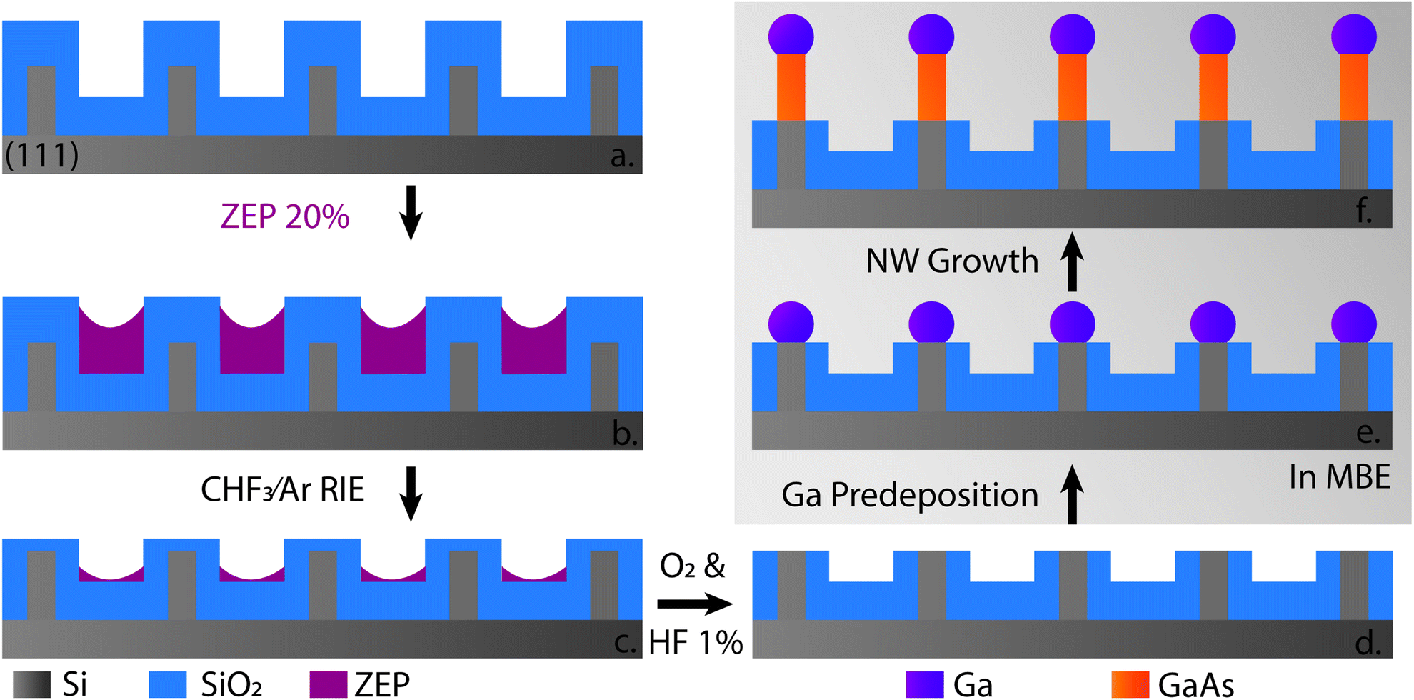 | ||
| Fig. 1 Schematic detailing the fabrication steps of SiO2/Si(111) pillars for self-catalyzed VLS GaAs NW growth. (a and b) The resist spin-coating process, (b and c) The RIE step and (c and d) the last wet etching before MBE loading. (e) Shows the very critical Ga predeposition step followed by (f) showing NW growth. | ||
The sample is then loaded in the MBE for vapor-phase growth. Fig. 1e represents the Ga predeposition step that forms the liquid catalyst droplet necessary for VLS. A constant Ga flux is sent to the substrate and Ga selectively aggregates at the Si pillar core, forming a droplet. The predeposition time, i.e. the time during which Ga flux is on, as well as the substrate temperature,24 determine the droplet volume. This step is crucial as the volume of the droplet is one of the determining parameters for the contact angle, defined as β, discussed later in this section. The liquid catalyst configuration was thoroughly characterized prior to NW growth by performing a predeposition-only growth with identical Ga fluxes and time.
Fig. 2a is a scanning electron microscopy (SEM) image at a 20° tilt angle of the NWs grown on 135 nm nominal diameter Si pillars with a 50 nm nominal oxidation. Fig. 2b shows the yield as a function of the pillar nominal diameter for the growth shown in a. named growth 1. It is worth noting that the nominal diameter differs from the real pillar diameter due to EBL dose/development (real size 20% smaller for sizes <100 nm diameter and 10% smaller for larger pillars until 300 nm diameter) and oxygen incorporation during oxidation (the SiO2 volume is 2.25 times that of Si25). For growth 1, the set manipulator temperature was 610 °C. Predeposition time was set at 15 min with a Ga beam equivalent pressure (BEP) of 2.1 × 10⁻⁷ Torr. We subsequentially open As for a V/III ratio of 11 for 30 min. Fluxes are then stopped and the substrate is cooled down to 100 °C.
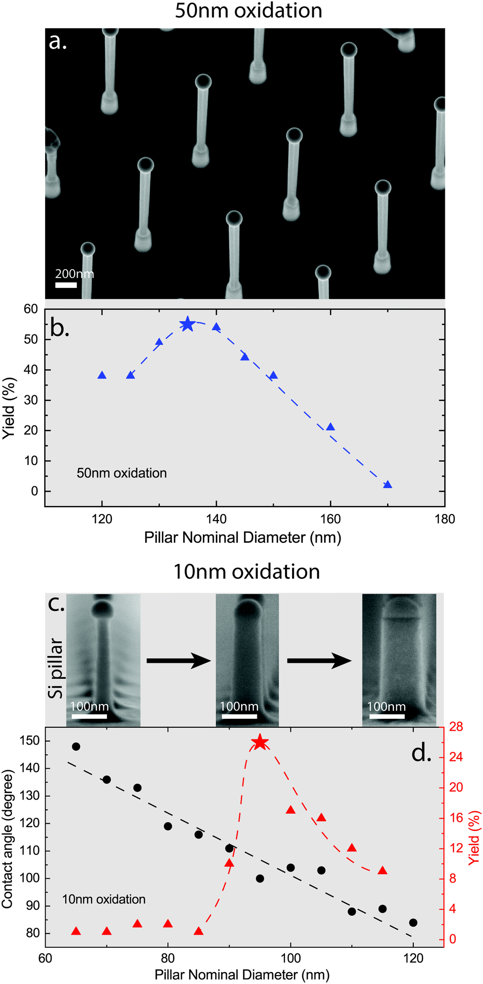 | ||
| Fig. 2 Aspects and statistics of NW growths done on EBL-patterned SiO2/Si pillars. (a) SEM image (20° tilt) showing vertical GaAs NWs grown on SiO2/Si (111) pillars. (b) Vertical yield as a function of pillar nominal diameter. (c) SEM images showing Ga droplets on top of SiO2/Si pillars of different nominal diameters. (d) Contact angle and yield as a function of pillar nominal diameter for pillars as shown in c. The optimum contact angle is identified as the one showing the best vertical yield. | ||
Fig. 2a gives us information about the growth mechanisms and growth selectivity; a Ga droplet is visible on top of each GaAs NW, confirming the VLS growth mechanism, and no parasitic growth is visible on the oxide mask, confirming the expected selectivity for NW arrays. Each vertical nanowire starts from a SiO2/Si pillar, which indicates a good selectivity. NWs possess a slight inverse tapering due to a Ga droplet volume increase during growth.24
Fig. 2b informs us about the evolution of the vertical yield with respect to pillar diameter. The average was calculated on areas of ∼2200 μm2 for each value. The curve shows a global maximum value at 55 ± 3% for a nominal diameter of 135 nm. This value then decreases steadily. We can link this behaviour with the study by Matteini et al.26 showing that vertical growth is initiated at an optimal β; as the entire substrate is exposed to the same Ga flux for the same amount of time, we assume the resulting droplet on top of every pillar has the same volume. After a certain volume threshold we also assume that the droplet is pinned at the SiO2/Si pillar sidewall. Therefore we expect very large β for smaller diameters and lower β for higher diameters. In this context, the vertical yield is maximized when the diameter of the SiO2/Si pillar permits the optimal β for vertical NW growth at the SiO2/Si interface.
The droplet contact angle β and its configuration on the SiO2/Si pillar is crucial for the growth. In order to study the Ga catalyst more in detail and verify our assumption, we measured droplets contact angles at various pillar diameters. Fig. 2c and d show measurements on pillars oxidized for a nominal thickness of 10 nm. Fig. 2c shows SEM images of SiO2/Si pillar cross-sections for the same predeposition time as growth 1. SEM images used for contact angle measurements of this figure can be found in the ESI.† The SiO2/Si pillars' nominal diameters are 65 nm, 100 nm and 135 nm. Fig. 2d shows both β (in black) and NW vertical yield (in red) as a function of the pillar nominal diameter for a second growth with the same conditions used in growth 1. The variation of β shows a linear decrease when increasing the pillar diameter. The maximum vertical yield is obtained for β = 100°. This value can be compared with the one of Matteini et al. where the optimum β value is 94°. The difference between both values can be explained by the Ga droplet constraint; Matteini et al. experimented on flat SiO2 surfaces, whereas we use SiO2/Si pillar. The measurement method also exhibits an error of ±5°.
So far, we have shown that self-catalyzed VLS growth of GaAs NWs on SiO2/Si pillars is possible at a good yield. We drew attention to the importance of reaching β = 100° for maximizing vertical NWs. As we linked the droplet volume to a given predeposition time, we can expect a variation of the maximum vertical yield in SiO2/Si pillar diameter by changing the predeposition time. In Fig. 3 we show the comparative results of three different growths having predeposition times of 10 min, 15 min and 20 min. The rest of the parameters are identical to growth 1. Fig. 3a shows schematics that illustrate the shift in Ga droplet volume for a given β. We observe a shift of the maximum yield to higher SiO2/Si pillar nominal diameters by increasing the predeposition time, which corroborates the previous assumption. The SiO2/Si pillar geometry therefore permits to choose a desired NW diameter by tuning the predeposition time, which can be attractive for applications that couple optical/acoustic/microwave modes with NWs for higher efficiencies, such as photodetectors27 or solar cells.8 Nevertheless we observe a decrease in the maximum yield for a predeposition time of 20 min. We explain this by the fact that all three growths share identical conditions (apart from the predeposition time) for the sake of the experiment, and a larger droplet is expected to require a higher As flux for an optimum NW growth.
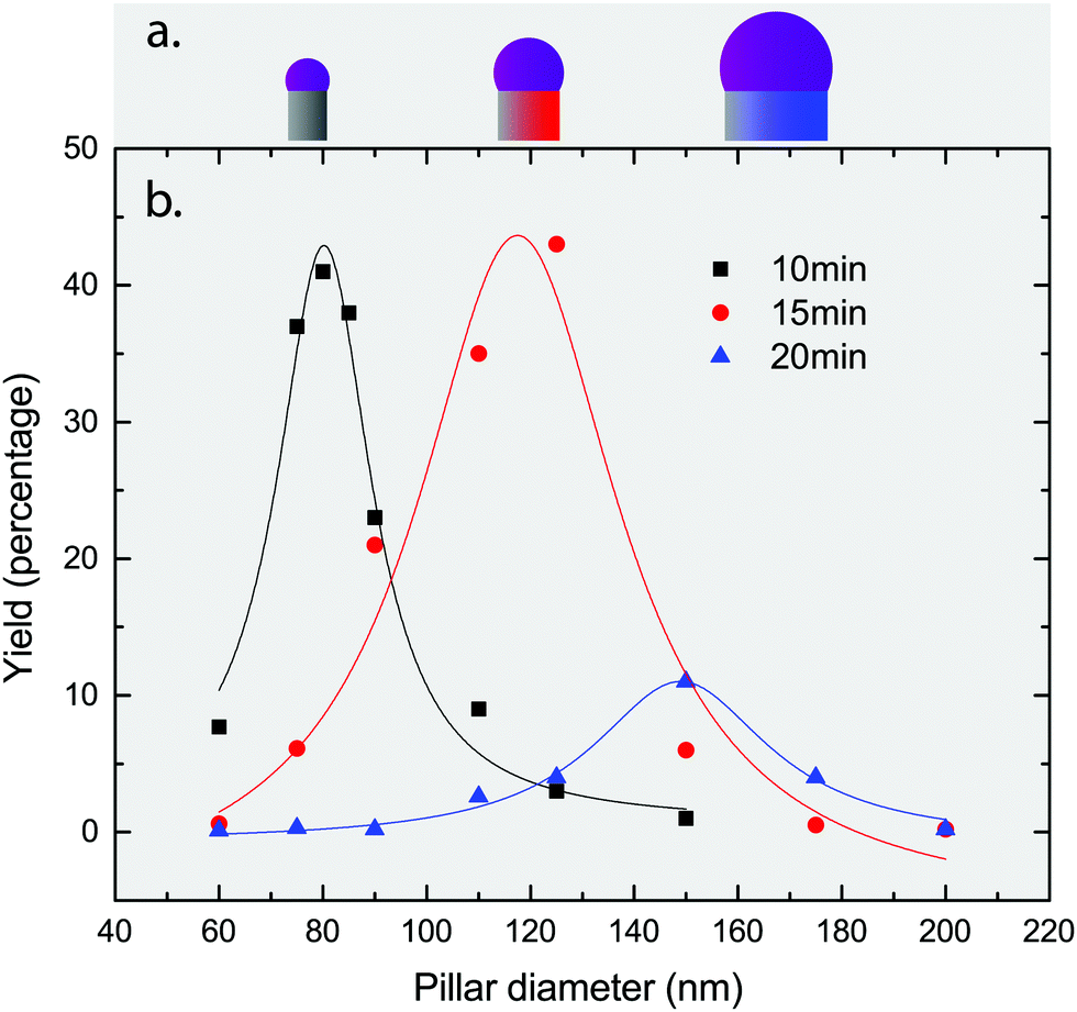 | ||
| Fig. 3 (a) Schematics showing the increase in droplet volume with SiO2/Si pillar diameter at a fixed contact angle. (b) Vertical yield as a function of SiO2/Si pillar nominal diameter for Ga predeposition times of 10 min, 15 min and 20 min. | ||
Coming back to Fig. 2b and d focusing on the yield curves for 50 nm and 10 nm oxidation: comparing the yield curves for 50 nm and 10 nm oxidation in Fig. 2b and d, respectively, we observe that, for identical growth conditions, the global maximum stands at different SiO2/Si pillar diameters. Its value also varies from 55% to 26%. We thus deduce that there is an influence of the oxide thickness on the maximum yield and optimum SiO2/Si diameter. We develop this hypothesis in Fig. 4 by showing a comparative study of three different growths identical to growth 1, but on substrates oxidized for nominal thicknesses of 10 nm, 30 nm and 50 nm. The Ga predeposition time and flux being fixed, we assume the Ga droplet volume is identical throughout the growths. We see that we have an increase in optimum SiO2/Si pillar diameter by increasing the oxide thickness. We link this with the fact that thicker nominal oxidations result in a reduction of the Si core.25 The Ga droplet volume being constant, β = 100° is reached at fixed Si core diameter, i.e. larger SiO2/Si nominal diameter for a higher nominal oxide thickness. This is illustrated in Fig. 4a where the Si core diameter at β = 100° for the three different oxidations is schematically illustrated.
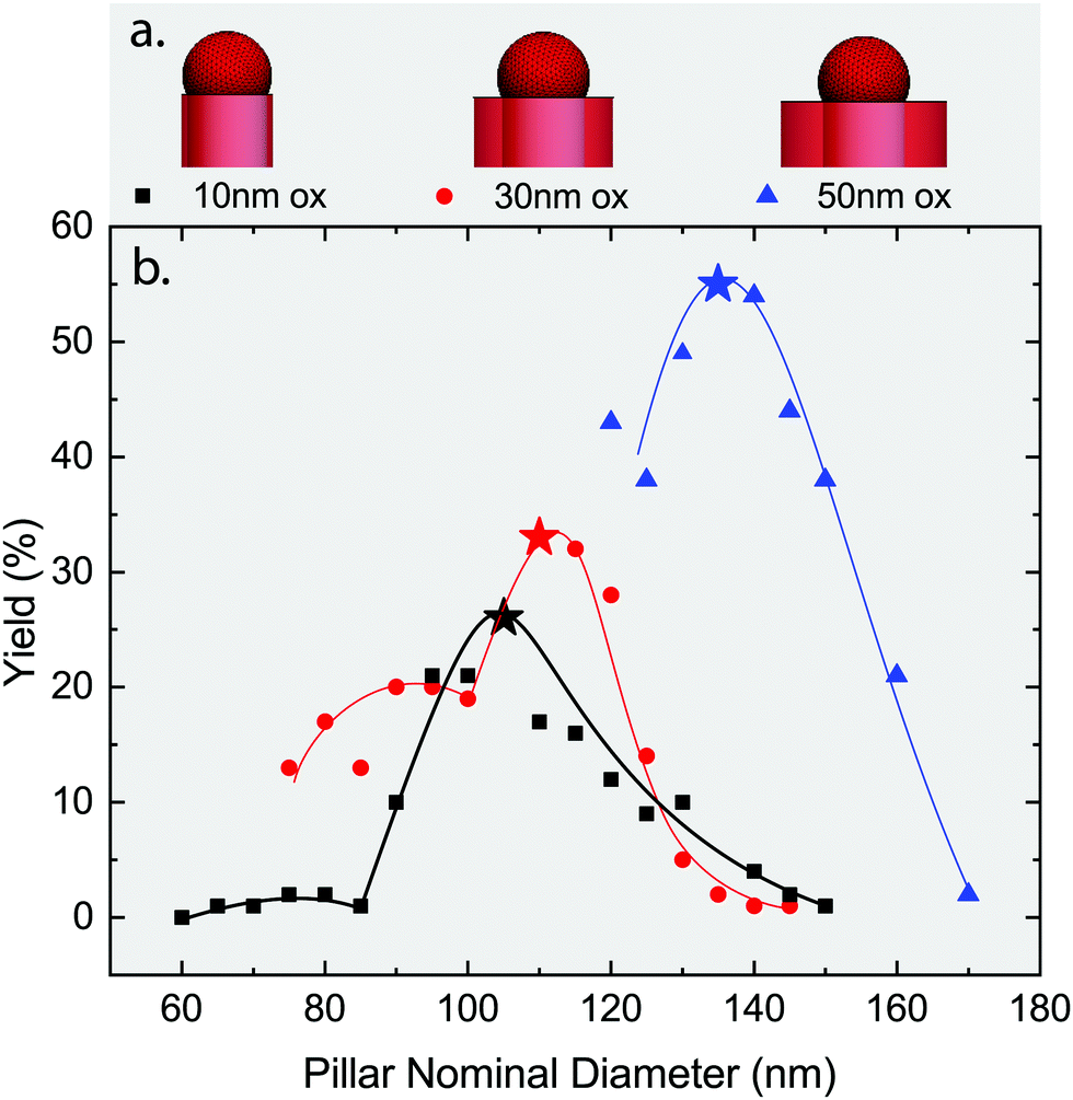 | ||
| Fig. 4 (a) Schematics showing the change in SiO2/Si pillar nominal diameter for a fixed Si core diameter and Ga dropelt volume. (b) Vertical yield as a function of the SiO2/Si pillar nominal diameter for nominal oxidations of 10 nm, 30 nm and 50 nm. | ||
We now focus on the increase of maximum yield with oxidation; Fig. 4b shows that increasing the oxide thickness around the Si core permits a higher yield. We explain this by studying the location of the triple phase line (TPL), i.e. the line that simultaneously separates liquid Ga, solid Si and vapor phases.28 We assume that the ideal droplet configuration for the vertical NW growth is β = 100° with the TPL at the SiO2/Si interface, i.e. the inner interface. During predeposition the droplet volume and β increase simultaneously on top of the Si core. After reaching the equilibrium β value for Si, i.e. 51°, the droplet pins at the SiO2/Si interface and swells until reaching the equilibrium β value for SiO2, i.e. 116°. Further swelling, firstly, moves the TPL away from the Si core by keeping β = 116°. Secondly, the droplet pins to the pillar side and continues swelling, increasing β to out-of-equilibrium values, as seen in Fig. 2d. We believe a thicker oxide permits to stabilize the TPL close to the Si core with β relatively close to 100°.
In order to visualize such droplet evolution, we performed simulations using the software Surface Evolver™, which permits one to study the shape of liquid surfaces under the effect of different energies and constraints. We computed the equilibrium shape of the liquid and verified the development of the surface energy of the system as a function of the droplet volume. In Fig. 5 we show six different curves of the apparent droplet angle as a function of the droplet volume for different dSiO2/dSi ratios, keeping dSi constant, dSiO2 being the oxide thickness and dSi the Si thickness on a pillar diameter. We observe three main evolution regimes: the initial steep increase for very small diameters corresponding to the swelling with the TPL at the SiO2/Si interface. All dSiO2/dSi ratios share the same curve in this regime, as dSi defines the critical volume for the onset of the first pinning. The second regime is a plateau at the equilibrium β = 116° value for SiO2. The length of this plateau depends on dSiO2/dSi: the thicker the oxide, the longer the plateau. We attribute this evolution to the free increase of the droplet volume with the TPL on the SiO2. Therefore this regime covers a larger range of volumes for a higher dSiO2/dSi ratio. The third regime corresponds to the second pinning at the pillar side wall where β increases again. The simulations are in agreement with experiments, showing that thicker oxides exhibits a contact angle relatively close to 100° for a larger droplet volume window.
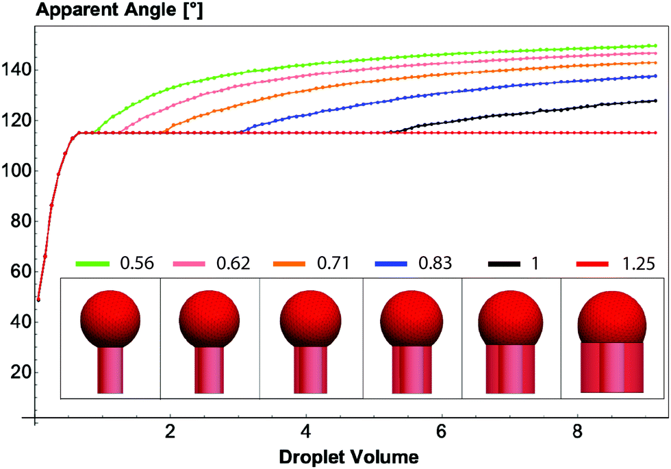 | ||
| Fig. 5 Results of simulations done on Surface Evolver™. The graph shows the droplet apparent angle, i.e. contact angle, for dSiO2/dSi ratios of 0.56, 0.62, 0.71, 0.83, 1 and 1.25. | ||
This study on EBL pillars permits us to understand the underlying mechanisms and critical parameters for maximizing the NW vertical yield; SiO2/Si pillars can be larger than 130 nm if oxidized properly and the predeposition time chosen accordingly to reach an initial β = 100°. These criteria open perspectives of large-scale implementation. In fact, pillars larger than 150 nm can be produced using industrial lithography techniques like PSL or DUVSL. The next section aims at growing large-scale GaAs NW arrays on SiO2/Si(111) pillars based on photolithographically defined patterns.
3 Photolithography
The next NW growths were performed on PSL pillars, though we present analogous arrays using DUVSL in the ESI.† PSL exposure was performed by EULITHA™ using their in-house Phable™ system, which is a displacement Tablot lithography system29,30 permitting periodic arrays of 130 nm features. The PSL technology allows for exposures lasting few seconds and can be expanded beyond 4 inches wafers. Subsequent RIE steps for anti-reflective coating and Si etching permitted to manufacture arrays shown in Fig. 6a. Fig. 6b shows the same array after dry oxidation, nominal planar thickness 70 nm at 1050 °C. The increase in volume due to oxygen incorporation is visible, as pillars exhibit a 50 nm increase in diameter after oxidation. Fig. 6c shows a cleaved SEM cross section of the pillars used for growth, with a nominal dry oxidation thickness of 160 nm at 1050 °C. This SEM image depicts the influence of geometry on oxidation; the top, side and planar thickness exhibit different values. This is explained by the oxygen incorporation rate and strain build-up inside the SiO2 for the pillar geometry.31–33 On Fig. 6c three coloured arrows indicate the local planar (blue), side wall (green) and top (red) oxide thickness.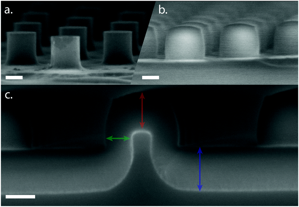 | ||
| Fig. 6 SEM images showing (a) PSL-patterned Si pillars after RIE, (b) after 70 nm nominal dry oxidation and (c) a cross-section of a SiO2/Si pillar after 160 nm dry oxidation. Scale bars are 100 nm. | ||
The array covers the entire 4-inch Si wafer. The potential for very large-scale NW arrays is clear and presented in Fig. 7. Fig. 7a shows a 2 cm × 2 cm chip used for the MBE growth fully covered by a 40% yield array. Local yield variations of ±10% happen between the center and the border due to edge effect during spin-coating.34 In fact, the spin-coating and the RIE steps depicted in Fig. 1 between a and c are critical for a proper pillar uncovering and droplet configuration. Fig. 7b illustrates this by showing an SEM image of a spin-coating comet, i.e. an irregularity in the spin-coated thickness due to an impurity, that locally exhibits a 67% yield whereas the rest of the chip did not give any growth. We believe this unveils the last key parameter in order to obtain 90+% yield arrays: the top SiO2/Si interface. If we over-etch, the droplet becomes unstable and does not grow into a NW. If we under-etch, Si is still covered by SiO2 which prevents growth completely. If the spin-coated polymer does not protect the SiO2 side-walls properly, RIE alters the shape of the pillar and impairs droplet stability. We believe that spin-coating a layer thicker than the pillar's height, planarizing it and controlling precisely the RIE are the key elements to obtain yields comparable to hole-based arrays.35,36
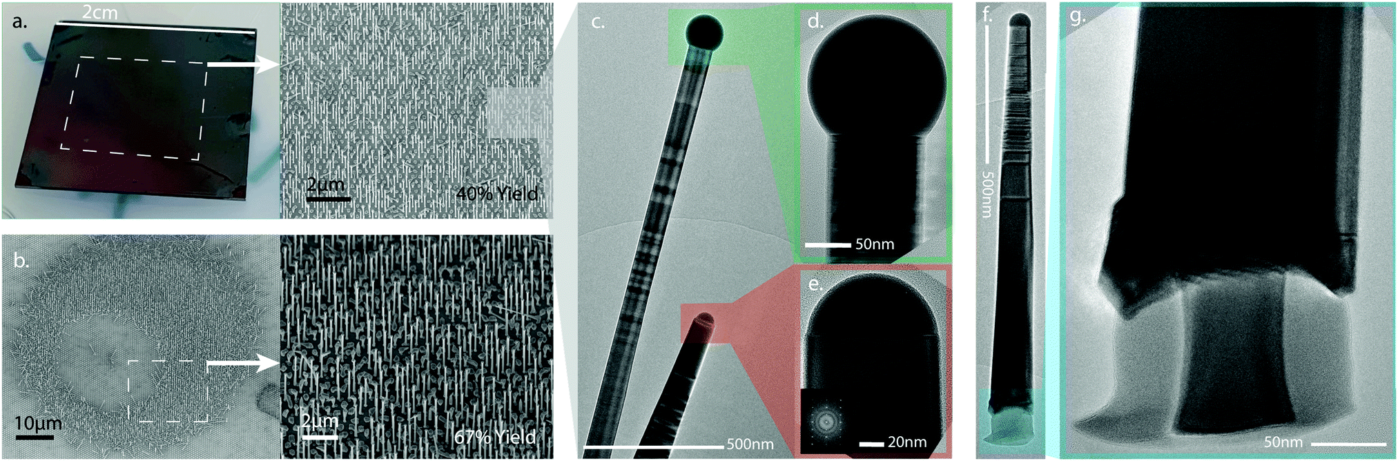 | ||
| Fig. 7 Self-catalyzed VLS growth of GaAs NWs on SiO2/Si (111) PSL pillars. (a) Large-scale array showing a 40% vertical yield. (b) Local vertical yield of 67% from a spin-coating comet. (c–e) TEM bright-field images of ZB and WZ nanowires coming from the same SiO2/Si large-scale array. The WZ FFT is visible. (f and g) WZ GaAs NW and the SiO2/Si pillar where it grew from. The pillar's Si core and SiO2 shell are visible. | ||
We now focus on the transmission electron microscopy (TEM) measurements presented in Fig. 7. Fig. 7c–g show the presence of ZB and WZ NWs simultaneously from the same growth. Whereas this was observed in the past from self-assembled growths,15 it was mainly through stochastic events and did not open perspectives for precise phase engineering. Many studies point out the correlation between droplet contact angle and NW crystal phase.28,37,38 Thanks to contact angle engineering from SiO2/Si pillar diameter and predeposition time tuning, the pillar geometry potentially permits to obtain either WZ NWs, ZB NWs or both at patterned locations in a deterministic way.
Fig. 7d shows a ZB GaAs NW with its characteristic Ga droplet configuration, i.e. >130° contact angle.37 We can also observe the presence of stacking faults that are frequently observed in 〈111〉 B NWs.39Fig. 7e shows a WZ GaAs NW with the image's fast-Fourier transform (FFT) confirming its phase.15Fig. 7f and g show the interface between a WZ NW and the SiO2/Si pillar from which it grew. The NW starts from the pillar sidewalls, which we believe is the reason for its WZ phase. In fact, as the Ga droplet un-pins from the SiO2/Si inner interface and pins to the outer SiO2 side-wall, for a given volume, the contact angle decreases drastically. This decreased contact angle appears nearly ideal for WZ NW growth, triggering pure WZ NWs. We even observed a short growth on 10 nm dry oxide SiO2/Si pillars where all the vertical NWs appear to be WZ, based on the morphology of the NW and the droplet configuration. This can be seen in the ESI.†
We have highlighted the advantage of using Si nanopillars as opposed to nanoscale holes for the successful integration of GaAs on Si. Our results highlight the importance of controlling the wetting behavior both in terms of contact angle and to position the triple phase line. In particular, we highlight the importance of the triple phase line located at the SiO2/Si interface as opposed to SiO2/vacuum or Si/vacuum. Nanopillars are an ideal platform to achieve such exquisite degree of control as well as large scalability on the silicon platform.
As these NWs appear to possess many similarities with NWs grown in nanohole arrays, for example the stacking fault density or Si/GaAs interface, we believe a more in-depth study of the impact of SiO2/Si pillars patterning on NWs crystal quality, doping and nucleation could be of interest. Methods such as In-situ TEM,40,41 cathodoluminescence and photoluminescence42–45 can shine light on these NWs nucleation mechanism and internal defect concentration.
4 Conclusion
In conclusion, we have highlighted the central importance of the Ga droplet contact angle and position of the triple phase line for reaching high vertical yield of GaAs nanowires, as well as also for crystal phase-selection. The SiO2/Si pillar geometry constitutes an ideal platform, allowing a precise and deterministic contact angle engineering and at the same time opening perspectives for reliable large-area patterning and freedom in design. This work brings NW arrays one step closer to large-scale implementation for devices.Methods/experimental
For EBL pillars: a 2 min 600 W O2 plasma in a TEPLATM GigaBatch is done on a 100 mm Si wafer for surface activation before spin coating with Dow Corning HSQ 006 and EBL exposure with a Vistec™ EBPG5000ES system. The dose used is 2740 μC cm−2 for all the pillar's diameters. The wafer is then developed using a commercial solution of MicropositR MFR CD26 for 2 minutes, and rinsed sequentially with water, acetone and propan-2-ol. A 2 min 600 W O2 plasma in a TEPLATM GigaBatch is done for further cross-linking the HSQ.For PSL pillars: after exposure at EULITHA™ using the PHABLE™ system, samples were shipped to EPFL for further processing. Sample is introduced in an SPTS APS plasma etcher where a plasma of CHF3/O2 of 20 s is done for anti-reflective coating etching.
The wafer, EBL or PSL, is then introduced in an AlcatelTM AMS200 DSE reactive ion etcher, where a customized recipe using SF6 and C4F8 is used for creating the pillars. A buffered hydrofluoric acid (7![[thin space (1/6-em)]](https://www.rsc.org/images/entities/char_2009.gif) :1) bath is then used for 2 minutes to remove any trace of resist. A thermal oxidation is then done at 1050 °C for a variable amount of time depending on the desired oxide thickness. The nominal oxide thickness mentioned throughout this study corresponds to the planar thickness obtained for a nominal oxidation time. After the oxide growth, a 50 nm Styrene Methyl Acrylate based resist (ZEP) film is spin coated and heated for 2 min at 180 °C for polymerization. Alternatively, a 170 nm thick poly methyl methacrylate (PMMA) can be used. The sample is inserted in an OxfordTM Plasmalab system 80 PLUS using a mixture of SF6 and CHF3 at 100 W plasma power for 40 seconds to uncover the pillars. 10 min of O2 plasma permits to remove the resist, and a last cleaning involving a 5 min acetone bath, a 2 min propan-2-ol bath and a 35 s HF bath at 1% concentration makes the sample ready for growth.
:1) bath is then used for 2 minutes to remove any trace of resist. A thermal oxidation is then done at 1050 °C for a variable amount of time depending on the desired oxide thickness. The nominal oxide thickness mentioned throughout this study corresponds to the planar thickness obtained for a nominal oxidation time. After the oxide growth, a 50 nm Styrene Methyl Acrylate based resist (ZEP) film is spin coated and heated for 2 min at 180 °C for polymerization. Alternatively, a 170 nm thick poly methyl methacrylate (PMMA) can be used. The sample is inserted in an OxfordTM Plasmalab system 80 PLUS using a mixture of SF6 and CHF3 at 100 W plasma power for 40 seconds to uncover the pillars. 10 min of O2 plasma permits to remove the resist, and a last cleaning involving a 5 min acetone bath, a 2 min propan-2-ol bath and a 35 s HF bath at 1% concentration makes the sample ready for growth.
The growths are conducted in a DCATM MBE chamber under a Ga BEP (beam equivalent pressure) of 0.21 × 10⁻⁶ Torr and an As BEP of 2.2 × 10⁻⁶ Torr for 45 minutes. The samples were characterized by SEM using a ZeissTM Merlin. NWs were transferred flat onto TEM copper grids and observed using an FEI Talos™ microscope for BF and HR images. The reported MBE growth temperatures are estimations of the substrate temperature. With measurements done with an infrared camera on known standard GaAs samples, we estimate a difference of 130 °C between the set PID and the real temperature.
Author contributions
Lucas G. took part in conceptualization, data curation, formal analysis, investigation, methodology, visualization, resources and writing. Lea G. took part in data curation, formal analysis, investigation, methodology and visualization. L. W., C. D. and H. S. took part in resources. N. M., D. D., J. B. L. and W. K. took part in methodology. A. B. took part in conceptualization, investigation, methodology and resources. R. M. took part in conceptualization, resources and validation. C. C. took part in conceptualization, supervision and validation. A. F. M. took part in conceptualization, funding acquisition, supervision, project administration and validation.Conflicts of interest
There are no conflicts to declare.Acknowledgements
L. G. thanks all the MBE team, but also the CMi staff at EPFL without whom none of this study could be possible. LG thanks EULITHA for the precious help in exposing the (111) Si wafers. We thank the SNF and QSIT for funding the project (projects 200021_169908 et IZLRZ2_163861).References
- K. Peng, P. Parkinson, Q. Gao, J. L. Boland, Z. Li, F. Wang, S. Mokkapati, L. Fu, M. B. Johnston, H. H. Tan and C. Jagadish, Single n + i–n + InP Nanowires For Highly Sensitive Terahertz Detection, Nanotechnology, 2017, 28(125202), 1–9 Search PubMed.
- Y. Cui, Q. Wei, P. Park, C. M. Lieber and H. Park, Nanowire Nanosensors for Highly Sensitive and Selective Detection of Biological and Chemical Species, Science, 2001, 293, 1289–1292 CrossRef CAS PubMed.
- S. Chuang, Q. Gao, R. Kapadia, A. C. Ford, J. Guo and A. Javey, Ballistic InAs Nanowire Transistors, Nano Lett., 2013, 13, 555–558 CrossRef CAS PubMed.
- V. Mourik, K. Zuo, S. M. Frolov, S. R. Plissard, E. P. A. M. Bakkers and L. P. Kouwenhoven, Signatures Of Majorana Fermions In Hybrid Superconductorsemiconductor Nanowire Devices, Science, 2012, 336, 1003–1007 CrossRef CAS PubMed.
- Z.-h. Liu and R. Li, Spin-relaxation Anisotropy In A Nanowire Quantum Dot With Strong Spin-orbit Coupling, AIP Adv., 2018, 8(075115), 1–9 Search PubMed.
- A. Manolescu, A. Sitek, J. Osca, L. Serra, V. Gudmundsson and T. D. Stanescu, Majorana States In Prismatic Core–shell Nanowires, Phys. Rev. B, 2017, 96(125435), 1–13 Search PubMed.
- D. I. Suh, S. Y. Lee, T. H. Kim, J. M. Chun, E. K. Suh, O. B. Yang and S. K. Lee, The Fabrication And Characterization Of Dye-sensitized Solar CellsWith A Branched Structure Of ZnO Nanowires, Chem. Phys. Lett., 2007, 442, 348–353 CrossRef CAS.
- P. Krogstrup, H. I. Jørgensen, E. Johnson, M. H. Madsen, C. B. Sørensen, A. F. I. Morral, M. Aagesen, J. Nygård and F. Glas, Advances In The Theory Of III–V Nanowire Growth Dynamics, J. Phys. D: Appl. Phys., 2013, 46, 313001 CrossRef.
- J. Wallentin, N. Anttu, D. Asoli, M. Huffman, I. Aberg, M. H. Magnusson, G. Siefer, P. Fuss-Kailuweit, F. Dimroth, B. Witzigmann, H. Q. Xu, L. Samuelson, K. Deppert and M. T. Borgström, InP Nanowire Array Solar Cells Achieving 13.8 percent Efficiency By Exceeding The Ray Optics Limit, Science, 2013, 339, 1057–1060 CrossRef CAS PubMed.
- S. Naureen, Top-down Fabrication Technologies for High Quality III–V Nanostructures, PhD thesis, KTH Royal Institute of Technology, 2013 Search PubMed.
- L. Güniat, P. Caroff and A. I. Fontcuberta Morral, Vapor Phase Growth of Semiconductor Nanowires: Key Developments and Open Questions, Chem. Rev., 2019, 119, 8958 CrossRef PubMed.
- A. Fontcuberta i Morral, C. Colombo, G. Abstreiter, J. Arbiol and J. R. Morante, Nucleation Mechanism Of Gallium-assisted Molecular Beam Epitaxy Growth Of Gallium Arsenide Nanowires, Appl. Phys. Lett., 2008, 92, 10–13 Search PubMed.
- J. Vukajlovic-Plestina, W. Kim, L. Ghisalberti, G. Varnavides, G. Tütüncuoglu, H. Potts, M. Friedl, L. Güniat, W. C. Carter, V. G. Dubrovskii and A. Fontcuberta i Morral, Fundamental Aspects To Localize Self-catalyzed III–V Nanowires On Silicon, Nat. Commun., 2019, 10, 869 CrossRef CAS PubMed.
- B. Bauer, A. Rudolph, M. Soda, A. Fontcuberta Morral, J. Zweck, D. Schuh and E. Reiger, Position Controlled Selfcatalyzed Growth Of GaAs Nanowires By Molecular Beam Epitaxy, Nanotechnology, 2010, 21, 435601 CrossRef PubMed.
- V. G. Dubrovskii, W. Kim, V. Piazza, L. Güniat and A. Fontcuberta i Morral, Simultaneous Selective Area Growth of Wurtzite and Zinc blende Self-Catalyzed GaAs Nanowires on Silicon, Nano Lett., 2021, 21, 3139–3145 CrossRef CAS PubMed.
- S. Plissard, G. Larrieu, X. Wallart and P. Caroff, High Yield Of Self-catalyzed GaAs Nanowire Arrays Grown On Silicon Via Gallium Droplet Positioning, Nanotechnology, 2011, 22(275602), 1–7 Search PubMed.
- P. Caroff, K. A. Dick, J. Johansson, M. E. Messing, K. Deppert and L. Samuelson, Controlled Polytypic And Twinplane Superlattices In III–V Nanowires, Nat. Nanotechnol., 2009, 4, 50–55 CrossRef CAS PubMed.
- M. Altissimo, E-beam lithography for micro-/nanofabrication, Biomicrofluidics, 2010, 4 Search PubMed.
- R. Jafari Jam, J. P. Beech, X. Zeng, J. Johansson, L. Samuelson, H. Pettersson and M. T. Borgström, Embedded sacrificial AlAs segments in GaAs nanowires for substrate reuse, Nanotechnology, 2020, 31 Search PubMed.
- A. M. Munshi, D. L. Dheeraj, V. T. Fauske, D. C. Kim, J. Huh, J. F. Reinertsen, L. Ahtapodov, K. D. Lee, B. Heidari, A. T. Van Helvoort, B. O. Fimland and H. Weman, Position-controlled Uniform GaAs Nanowires On Silicon Using Nanoimprint Lithography, Nano Lett., 2014, 14, 960–966 CrossRef CAS PubMed.
- E. Russo-Averchi, J. Vukajlovic Plestina, G. Tütüncüoglu, F. Matteini, A. Dalmau-Mallorquí, M. De La Mata, D. Rüffer, H. A. Potts, J. Arbiol, S. Conesa-Boj and A. Fontcuberta I Morral, High Yield Of GaAs Nanowire Arrays On Si Mediated By The Pinning And Contact Angle Of Ga, Nano Lett., 2015, 15, 2869–2874 CrossRef CAS PubMed.
- L. Güniat, S. Martí-Sánchez, O. Garcia, M. Boscardin, D. Vindice, N. Tappy, M. Friedl, W. Kim, M. Zamani, L. Francaviglia, A. Balgarkashi, J. B. Leran and J. Arbiol, Fontcuberta I Morral, A. III–V Integration on Si(100): Vertical Nanospades, ACS Nano, 2019, 13, 5833–5840 CrossRef PubMed.
- S. S. G. Varricchio, H. Cyrille, B. Arnaud and R. Philippe, Fabrication Of Multilayered Nanofluidic Membranes Through Silicon Templates, Nanoscale, 2015, 7, 20451–20459 RSC.
- A. Pishchagin, F. Glas, G. Patriarche, A. Cattoni and J.-C. Harmand, Dynamics of Droplet Consumption in Vapor–Liquid–Solid III–V Nanowire Growth, Crystal Growth Des., 2021, 21, 4647 CrossRef CAS.
- D. Shir, B. Z. Liu, A. M. Mohammad, K. K. Lew and S. E. Mohney, Oxidation of silicon nanowires, J. Vac. Sci. Technol., B: Microelectron. Nanometer Struct., 2006, 24, 1333 CrossRef CAS.
- F. Matteini, G. Tütüncüoglu, D. Mikulik, J. Vukajlovic-Plestina, H. Potts, J.-B. Leran, W. C. Carter and A. Fontcuberta I Morral, Impact Of The Ga DropletWetting, Morphology, And Pinholes On The Orientation Of GaAs Nanowires, Crystal Growth Des., 2016, 16, 5781–5786 CrossRef CAS.
- A. Dorodnyy, E. Alarcon-Lladó, V. Shklover, C. Hafner, A. Fontcuberta I Morral and J. Leuthold, Efficient Multiterminal Spectrum Splitting via a Nanowire Array Solar Cell, ACS Photonics, 2015, 2, 1284–1288 CrossRef CAS PubMed.
- F. Glas, J. C. Harmand and G. Patriarche, Why DoesWurtzite Form In Nanowires Of III–V Zinc Blende Semiconductors?, Phys. Rev. Lett., 2007, 99(146101), 1–4 Search PubMed.
- H. H. Solak, C. Dais, F. Clube and L. Wang, Phase shifting masks in Displacement Talbot Lithography for printing nanogrids and periodic motifs, Microelectron. Eng., 2015, 143, 74–80 CrossRef CAS.
- L. Wang, F. Clube, C. Dais, H. H. Solak and J. Gobrecht, Sub-wavelength printing in the deep ultra-violet region using Displacement Talbot Lithography, Microelectron. Eng., 2016, 161, 104–108 CrossRef CAS.
- D.-B. Kao, J. McVittie, W. Nix and K. Saraswat, Two-dimensional Thermal Oxidation Of Silicon. II. Modeling Stress Effects In Wet Oxides, IEEE Trans. Electron Devices, 1988, 35, 25–37 CrossRef.
- H. I. Liu, Oxidation Of Sub-50 nm Si Columns For Light Emission Study, J. Vac. Sci. Technol., B: Microelectron. Nanometer Struct., 1992, 10(2846), 1–5 Search PubMed.
- H. Cui, C. X. Wang and G. W. Yang, Origin Of Self-limiting Oxidation Of Si Nanowires, Nano Lett., 2008, 8, 2731–2737 CrossRef CAS PubMed.
- M. Tyona, A theoritical study on spin coating technique, Adv. Mater. Res., 2013, 2, 195–208 CrossRef.
- S. N. Piramanayagam, R. Sbiaa, E. L. Tan, A. W. C. Poh, H. K. Tan, K. O. Aung, J. Zhao and S. K. Wong, Planarization of patterned recording media, IEEE Trans. Magn., 2010, 46, 758–763 CAS.
- S. Büyükköse, B. Vratzov and W. G. van der Wiel, High-quality global hydrogen silsequioxane contact planarization or nanoimprint lithography, J. Vac. Sci. Technol., B: Nanotechnol. Microelectron.: Mater., Process., Meas., Phenom., 2011, 29, 021602 Search PubMed.
- F. Panciera, Z. Baraissov, G. Patriarche, V. G. Dubrovskii, F. Glas, L. Travers, U. Mirsaidov and J. C. Harmand, Phase Selection in Self-catalyzed GaAs Nanowires, Nano Lett., 2020, 20, 1669–1675 CrossRef CAS PubMed.
- W. Kim, V. Dubrovskii, J. Vukajlovic-Plestina, G. Tütüncüoglu, L. Francaviglia, L. Güniat, H. Potts, M. Friedl and J.-B. Leran, Fontcuberta I Morral, A. Bistability of Contact Angle and Its Role in Achieving Quantum-Thin Self-Assisted GaAs nanowires, Nano Lett., 2018, 18, 49 CrossRef CAS PubMed.
- M. Zamani, G. Tütüncüoglu, S. Martí-Sánchez, L. Francaviglia, L. Güniat, L. Ghisalberti, H. Potts, M. Friedl, E. Markov, W. Kim, J.-B. Leran, V. G. Dubrovskii, J. Arbiol and A. Fontcuberta i Morral, Optimizing The Yield Of Apolar Gaas Nanowires To Achieve Defectfree Zinc Blende Structure And Enhanced Optical Functionality, Nanoscale, 2018, 10, 17080–17091 RSC.
- D. Jacobsson, F. Panciera, J. Tersoff, M. C. Reuter, S. Lehmann, S. Hofmann, K. A. Dick and F. M. Ross, Interface dynamics and crystal phase switching in GaAs nanowires, Nature, 2016, 531, 317–322 CrossRef CAS PubMed.
- F. M. Ross, J. Tersoff and M. C. Reuter, Sawtooth Faceting In Silicon Nanowires, Phys. Rev. Lett., 2005, 95, 1–4 Search PubMed.
- W. Kim, L. Güniat, A. Fontcuberta I Morral and V. Piazza, Doping challenges and pathways to industrial scalability of III–V nanowire arrays, Appl. Phys. Rev., 2021, 8, 011304 CAS.
- D. Spirkoska, J. Arbiol, A. Gustafsson, S. Conesa-Boj, F. Glas, I. Zardo, M. Heigoldt, M. H. Gass, A. L. Bleloch, S. Estrade, M. Kaniber, J. Rossler, F. Peiro, J. R. Morante, G. Abstreiter, L. Samuelson and A. Fontcuberta I Morral, Structural And Optical Properties Of High Quality Zinc blende/wurtzite GaAs Nanowire Heterostructures, Phys. Rev. B: Condens. Matter Mater. Phys., 2009, 80, 1–9 CrossRef.
- H. L. Chen, C. Himwas, A. Scaccabarozzi, P. Rale, F. Oehler, A. Lemaître, L. Lombez, J. F. Guillemoles, M. Tchernycheva, J. C. Harmand, A. Cattoni and S. Collin, Determination of n-Type Doping Level in Single GaAs Nanowires by Cathodoluminescence, Nano Lett., 2017, 17, 6667–6675 CrossRef CAS PubMed.
- F. Martelli, M. Piccin, G. Bais, F. Jabeen, S. Ambrosini, S. Rubini and A. Franciosi, Photoluminescence Of Mncatalyzed GaAs Nanowires Grown By Molecular Beam Epitaxy, Nanotechnology, 2007, 18(125603), 1–4 Search PubMed.
Footnote |
| † Electronic supplementary information (ESI) available. See DOI: 10.1039/d1nh00553g |
| This journal is © The Royal Society of Chemistry 2022 |