
Magnetoconductance modulations due to interlayer tunneling in radial superlattices†
Yu-Jie
Zhong
ab,
Angus
Huang
acd,
Hui
Liu
e,
Xuan-Fu
Huang
a,
Horng-Tay
Jeng
 cdf,
Jhih-Shih
You
g,
Carmine
Ortix
hi and
Ching-Hao
Chang
*ab
cdf,
Jhih-Shih
You
g,
Carmine
Ortix
hi and
Ching-Hao
Chang
*ab
aDepartment of Physics, National Cheng Kung University, Tainan 70101, Taiwan. E-mail: cutygo@phys.ncku.edu.tw
bCenter for Quantum Frontiers of Research & Technology (QFort), National Cheng Kung University, Tainan 70101, Taiwan
cDepartment of Physics, National Tsing Hua University, Hsinchu 30013, Taiwan
dCenter for Quantum Technology, National Tsing Hua University, Hsinchu 30013, Taiwan
eIFW Dresden and Würzburg-Dresden Cluster of Excellence ct.qmat, Helmholtzstrasse 20, 01069 Dresden, Germany
fInstitute of Physics, Academia Sinica, Taipei 11529, Taiwan
gDepartment of Physics, National Taiwan Normal University, Taipei 11677, Taiwan
hInstitute for Theoretical Physics, Center for Extreme Matter and Emergent Phenomena, Utrecht University, Princetonplein 5, NL-3584 CC Utrecht, The Netherlands
iDipartimento di Fisica “E. R. Caianiello”, Universitá di Salerno, IT-84084 Fisciano, Italy
First published on 10th December 2021
Abstract
Radial superlattices are nanostructured materials obtained by rolling up thin solid films into spiral-like tubular structures. The formation of these “high-order” superlattices from two-dimensional crystals or ultrathin films is expected to result in a transition of transport characteristics from two-dimensional to one-dimensional. Here, we show that a transport hallmark of radial superlattices is the appearance of magnetoconductance modulations in the presence of externally applied axial magnetic fields. This phenomenon critically relies on electronic interlayer tunneling processes that activate an unconventional Aharonov–Bohm-like effect. Using a combination of density functional theory calculations and low-energy continuum models, we determine the electronic states of a paradigmatic single-material radial superlattice – a two-winding carbon nanoscroll – and indeed show momentum-dependent oscillations of the magnetic states in the axial configuration, which we demonstrate to be entirely due to hopping between the two windings of the spiral-shaped scroll.
New conceptsSuperlattices—artificial material structures with a nanoscale period—are generally characterized by nontrivial electronic states without counterparts in bulk crystals. The presence of these unique electronic states is reflected in the occurrence of novel and tunable transport properties of paramount importance both for fundamental science and for nanotechnology applications. Radial superlattices obtained by rolling up thin films represent a promising avenue to explore the potential of such artificial materials. Here, using a combination of density functional theory calculations and quantum continuum models, we show for the first time a characteristic transport property of radial superlattices: the occurrence of magnetoconductance oscillations due to externally applied axial magnetic fields. In particular, we demonstrate that the unconventional momentum-dependent oscillations of the magnetic-state energies entirely relies on interlayer tunneling processes – a tunable energy band characteristic in materials design. The work we undertook not only shows an exotic genre of electronic states and nontrivial robust transport properties in radial superlattices but also provides new insights for the design of superlattices in the laboratory. Our study thus provides a new route to engineer exotic electronic structures with rich application potential in the carbon neutral industry or to boost the processing performance of memory devices in intelligence technology. |
Since the pioneering work of Esaki and Tsu back in 1970,1 superlattices have introduced a new paradigm for the synthesis of artificial nanoscale material structures with tailored electronic properties. The synthesis of moiré superlattices of two-dimensional van der Waals materials, obtained for instance by placing single-layer graphene on aligned hexagonal boron nitride substrates,2–6 has led to the experimental observation of superlattice minibands forming the well-known Hofstadter butterfly7 and the related generation of Dirac cone replicas.8–13 Likewise, the moiré superlattice of magic-angle twisted bilayer graphene has been to shown to yield flat bands associated with emerging correlated insulating behavior and superconductivity.14,15 Rolled-up nanotechnology16–19 – a strain-induced technique able to tune planar ultrathin films into complex three-dimensional nanoarchitectures – provides yet another route to superlattices. The rolling-up mechanism can be applied to a huge variety of materials, including metals, insulators, polymers and traditional semiconductor families. Functional properties such as thermal conductivity have been shown to be geometrically tailored in silicon radial superlattices.20 Very recently, rolled-up nanotechnology has been also applied to two-dimensional van der Waals materials to create high-order van der Waals superlattices.21 Independent of the material in hand, the preparation of these material structures is expected to modulate their electronic properties via the effective change of dimensionality, thereby leading to unconventional transport behavior. For instance, a distinctive property of tubular structures with spiral-like cross sections is that they break the rotational symmetry in the embedding three-dimensional space. As a result, their longitudinal magnetoresistance can exhibit a marked directional dependence.22 This angle-dependent magnetoresistance has been predicted to occur in the ballistic regime when considering rolled-up nanotubes made out of conventional semiconducting materials. The same effect is expected to appear,23 however, also in the diffusive regime characterizing the transport in, e.g., carbon nanoscrolls: spirally wrapped graphite layers.24 The report of an angle-dependent magnetoresistance behavior in SnS2/WSe2 rolled-ups has provided experimental evidence for the occurrence of this geometry-induced effect.21 The aim of this work is to show that another transport hallmark of radial superlattices is the appearance of magnetoconductance modulations in the presence of externally applied axial magnetic fields.
When subject to axial magnetic fields, tubular structures with cross-sections forming closed loops display the well-known Aharonov–Bohm (AB) effect,25 which leaves distinctive fingerprints. Aharonov–Bohm (AB) magnetoresistance oscillations have been reported in multiwalled carbon nanotubes (CNTs).26 Furthermore, the AB effect has been predicted to induce a semimetal to semiconductor transition in single-walled CNTs.27,28 Distinctive signatures of the structural symmetry of semiconducting core–shell nanowires can be also inferred from the AB oscillations of the energy levels.29 Finally, characteristic fingerprints of the anomalous metallic states in three-dimensional topological insulator nanowires30 can be also identified from their associated AB effect.
The open cross section of a radial superlattice prevents a full phase interference between electronic waves traveling in the opposite direction at the origin of the AB effect. Any magnetoconductance oscillations in an axial configuration should be therefore completely prevented. Contrary to such expectations, we will instead show that radial superlattices can and do display magnetoconductance oscillations when an axial magnetic field is externally applied. Using the combination of density functional theory and an effective continuum low-energy model, we will theoretically prove that a carbon nanoscroll (CNS) – a prototypical radial superlattice – displays oscillations of the energy levels when subject to an axial magnetic field even in a minimal two-winding geometry. This effect is entirely due to the tunneling between the two consecutive windings of the spiral structure as proved by the fact that the energy level oscillations disappear by artificially switching off the interlayer coupling. We furthermore prove that the amplitude of the energy level oscillations is strongly dependent upon the momentum in the translationally invariant axial direction of the scroll.
We start out by illustrating the mechanism responsible for the onset of magnetoconductance oscillations in a spiralling two-winding carbon nanoscroll. Its geometry is explicitly shown in Fig. 1(a). Note that the axial, translationally invariant direction corresponds to a zigzag direction of the honeycomb lattice. As shown in Fig. 1(b) and (c) the interlayer structure is equivalent to the Bernal AB stacking in bilayer graphene. Therefore, the largest hopping amplitude in the structure corresponds to the interlayer hopping between “dimer” sites [see Fig. 1(c)]. Consider now the unrolled nanostructure along the azimuthal direction as shown in Fig. 1(d). The strong dimerization between the two layers implies that at each azimuthal angle the electronic wavefunction has a sizable probability amplitude on both the lower and the upper graphene layers. At the open edges explicitly marked in Fig. 1(d), on the other hand, the lower and upper graphene layers have to continuously evolve one into the other in order to reconstruct a two-winding scroll. Consequently, the dimerized electronic wavefunction is “partially” embedded in a closed geometry. Therefore, and as a result of the interlayer tunneling, the system can react to an electromagnetic potential precisely as in the conventional AB effect.
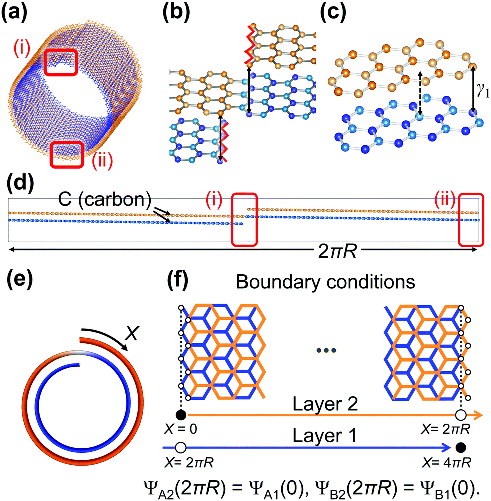 | ||
| Fig. 1 The structure and boundary conditions of two-winding CNSs. (a) The inner layer, layer 1 (outside layer, layer 2), of CNSs is illustrated by a blue (orange) line. (b) Zoom-in on the region (i) in (a). Layer 1 and layer 2 present a zigzag edge, highlighted by a red polygonal line. The edges are separated by the connecting region of layer 1 and layer 2. The black arrows are the relative positions of carbon ions. (c) Zoom-in on the region (ii) in (a). The interlayer coupling is γ1. (d) The unit cell, the flattened geometry of CNSs in (a), has the same topological structure as CNSs. (e) The cross-section with arc length X and (f) the boundary conditions for the continuum model of two-winding CNSs are shown. Atoms A1 (A2) and B1 (B2) are on the first (second) layer. | ||
To concretely prove the appearance of such an unconventional AB effect, we model a two-winding CNS with the low-energy k·p of bilayer graphene along the arclength (X axis) of the nanostructure while concomitantly using special boundary conditions that allow tunneling between the two layers (see Fig. 1(e) and (f)).
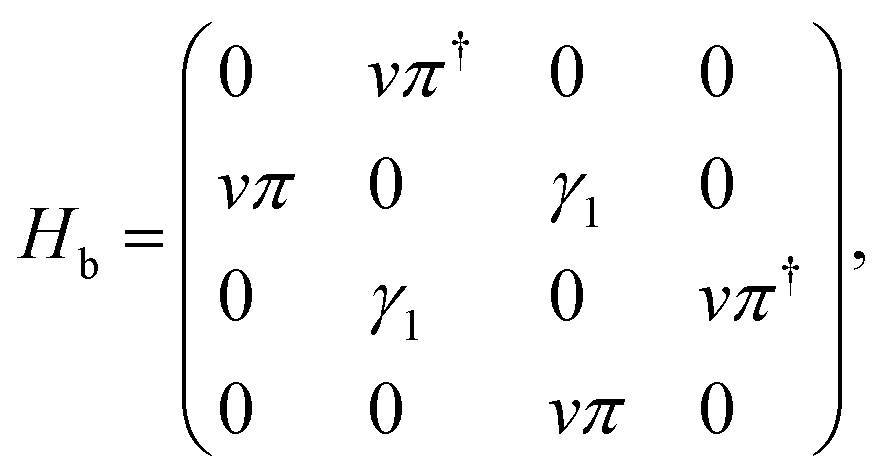
Specifically we use the effective four band model for the 2pz orbitals on the four atomic sites A1, B1, A2, and B2 of the unit cell. It can be written as follows:31
 | (1) |
 , where γ0 is the intralayer hopping amplitude between sites A1 and B1 (or A2 and B2). Finally, we explicitly consider the interlayer coupling between the dimer sites A2 and B1 γ1, as shown in Fig. 1.
The energy ε for eqn (1) is given by 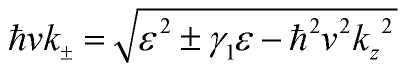 , where ± distinguishes between the valence and conduction bands. Furthermore, the left-moving L and right-moving R wave functions read
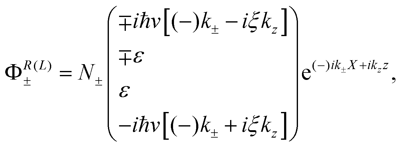 | (2) |
Within our continuum model, the electronic band structure of the two-winding CNS can be obtained by superimposing the boundary conditions shown in Fig. 1(f). They are given by
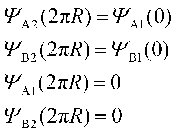 | (3) |
To fit the boundary conditions in eqn (3), we write a generic wave function Ψ, which is a combination of the left-moving L and right-moving R wave functions in the conduction and valence bands ΦR(L)±. In other words, we write the generic wave function as Ψ = aΦL+ + bΦL− + cΦR+ + dΦR−, where a, b, c, and d are the coefficients that we fix by imposing the boundary conditions.
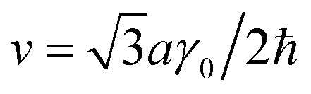
We also use the following microscopic tight-binding parameters: the lattice constant is a = 2.46 Å,32 whereas the intralayer and interlayer couplings are γ0 = 3.16 eV and γ1 = 0.381 eV, respectively.31,33 We also take the arclength of each layer L = 50 nm. Thus the total arclength of the two-winding nanoscroll is W = 100 nm.
Fig. 2(a) shows the energy bands of the two-winding CNSs obtained from our continuum model. kz = 0 is the projection of the high-symmetry K point, i.e. the Dirac point in monolayer graphene. In perfect analogy with the states found in graphene nanoribbons with zigzag edges, we find that also our two-winding carbon nanoscroll displays edge states for kz < 0 momenta [see Fig. 2(a)]. The density profiles of edge and bulk-like states and their kz-dependent evolutions are provided in the ESI† (Section S1). In order to establish that the continuum model provides an accurate description of the electronic structure of a two-winding CNS, we have thereafter performed density functional theory (DFT) calculations using the structure shown in Fig. 1(a)–(d). We provide the details of the DFT calculations in the ESI† (Section S2). As demonstrated in Fig. 2, there is an excellent agreement between the electronic structure obtained using DFT and our effective k·p model. This consequently allows the study on the effect of an externally applied axial magnetic field using the low-energy model.
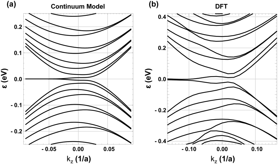 | ||
| Fig. 2 Energy bands of the two-winding CNS for the K point. (a) The perimeter is L = 50 nm for the continuum model and L = 20 nm for DFT.34 | ||
To investigate the effect of an externally applied homogeneous axial magnetic field, generally, we use a minimal coupling with the vector potential, A, related to the externally applied axial magnetic field by B = ∇ × A. Since the applied axial magnetic field is considered, B||ẑ, we introduce the canonical momenta k±′ given by 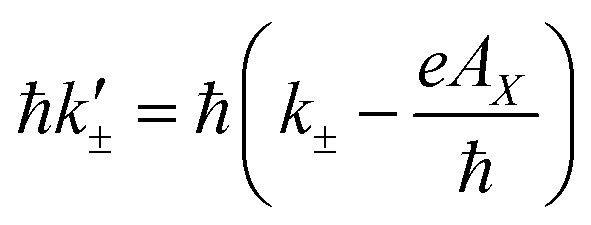 . The vector potential can be expressed generally as
 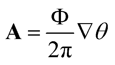 , where Φ is the magnetic flux and θ is the angle around the cylinder,35 and more clearly it is given as
 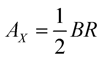 .22 Thus, we have that the wave factors in the wave functions with applied magnetic field must be written as
 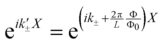 and
and 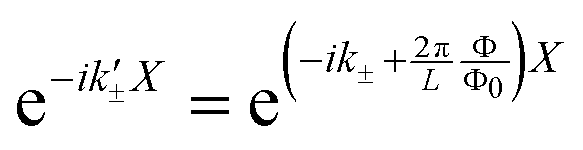 . Here we introduced the flux quantum which is given by
 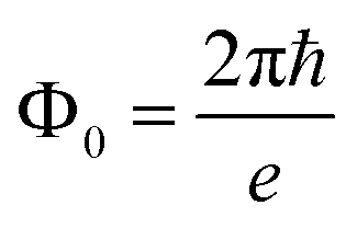 with e being the electronic charge.
Fig. 3 shows our main finding, that is, the oscillations of the energy levels as a function of the axial magnetic field intensity for different values of the transversal momentum kz in a structure where the conventional AB effect is precluded. Note that the amplitude of the oscillations is enhanced for kz > 0 and more attenuated by decreasing the longitudinal momentum toward the kz < 0 region.
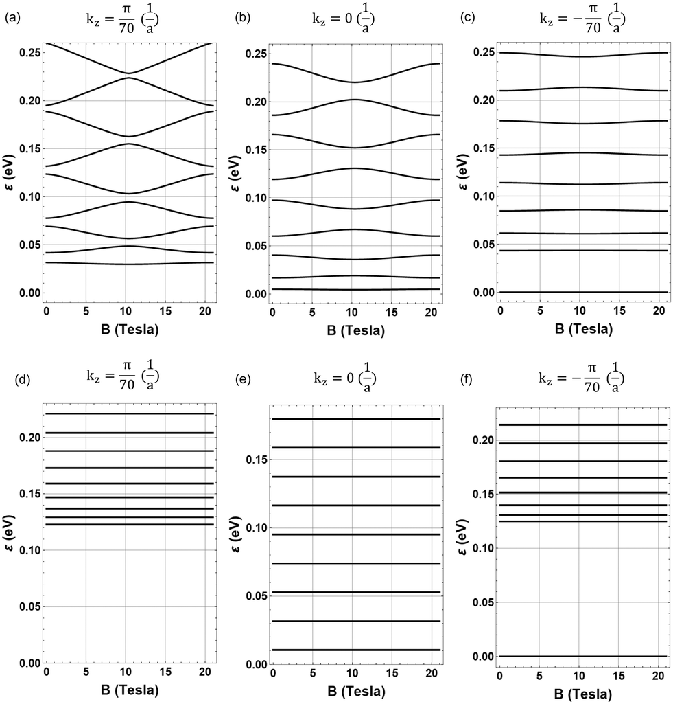 | ||
Fig. 3 Energy level ε vs. axial applied magnetic field B at different kz values. It is shown that the Aharonov–Bohm effect is present in two-winding CNSs. (a) to (c) are with the interlayer coupling γ1 = 0.381 eV.  is varied from 0 to 1 with flux quantum: Φ0 = 4.136 × 10⁻¹⁵ V s. (d) to (f) are without the interlayer coupling γ1. is varied from 0 to 1 with flux quantum: Φ0 = 4.136 × 10⁻¹⁵ V s. (d) to (f) are without the interlayer coupling γ1. | ||
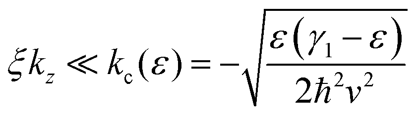
This result indicates that the electronic states with kz < 0 in the nanoscroll are similar in nature to the states in a flat “unrolled” bilayer graphene nanoribbon which, due to the open geometry, are not expected to display energy oscillations. As proved in the ESI† (Sections S4 and S6) these states without oscillations of the magnetic energy levels satisfy the following criterion on their tube axis momentum:
 | (4) |
In Fig. 3 we also present the magnetic energy states by artificially neglecting the dimer interlayer hopping amplitude γ1. The magnetic oscillations of the energy levels are completely absent, thus demonstrating that the presence of our unconventional AB effect in a spiral open structure is entirely due to the electronic tunneling between the layers.
We finally evaluate the consequence of the oscillations of the magnetic energy levels in transport. In particular, we consider the two-terminal conductance in the ballistic regime. We therefore use the Landauer formula:22,36,37
 | (5) |
We show the behavior of the conductance in the absence and presence of an axial magnetic field in Fig. 4. The oscillations of the magnetic energy levels is reflected in a finite magnetoconductance as evidenced by the change of ballistic conductance as the field strength is varied. In Fig. 4(a), for the low temperature and without applied magnetic field case (10 K and 0 Tesla), the widths of plateaux vary alternatively between large and small values. It is similar to the magnetic case; yet for the magnetic field case (10 K and 10 Tesla), the plateaux change their narrow ones to broad, and vice versa. Similar phenomena occur at a high temperature (50 K) (Fig. 4(b)) and a medium temperature (25 K) (Fig. S10 in the ESI†). In the low-temperature regime, we have the conventional quantization in units of 2e2/h of a quantum point contact38 with different plateaux as we sweep the Fermi energy (see Fig. 4(a)). The difference in the plateau structures in the presence of the axial magnetic field is the fingerprint of the magnetoconductance modulations. Note that the axial magnetic field effects on the two-terminal conductance persist even in the high temperature regime where the quantization of the conductance is lost due to the thermal smearing, as is shown in Fig. 4(b).
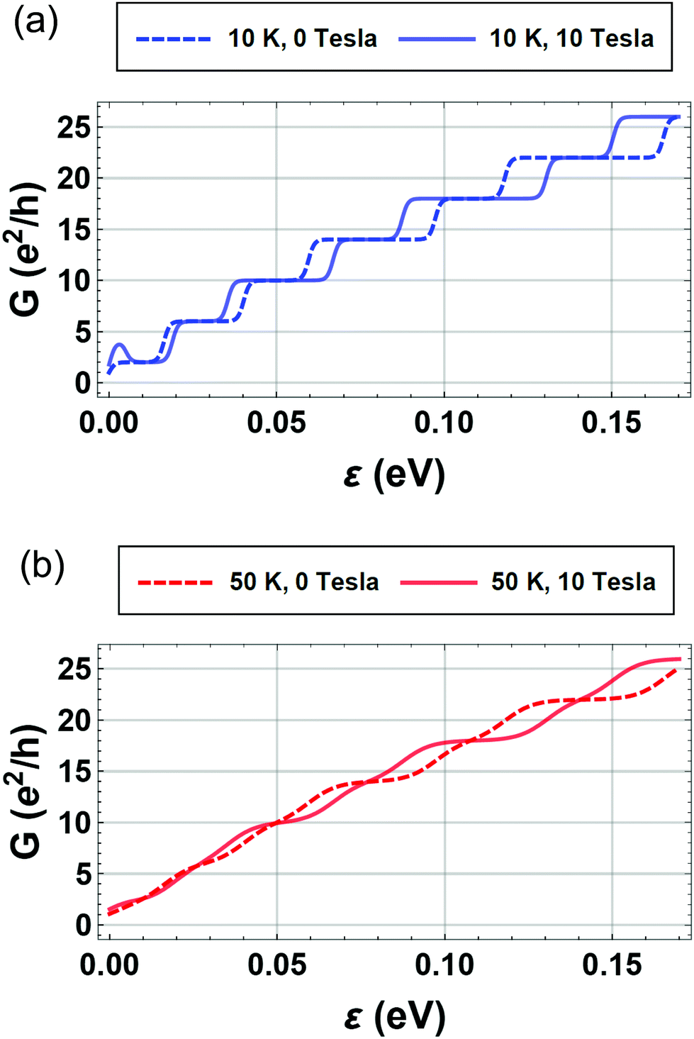 | ||
| Fig. 4 The conductance of two-winding carbon nanoscrolls for (a) a low temperature (10 K) and (b) a high temperature (50 K). The dashed line indicates the applied magnetic field B = 0 Tesla, whereas the solid line is for B ≈ 10 Tesla (10.3949 Tesla in the numerical calculation). | ||
To wrap up, we have considered a combination of DFT calculations and an effective low-energy k·p model, the electronic properties of a two-winding CNS, and established, in the presence of an axial magnetic field, the occurrence of oscillations of the magnetic energy levels as the intensity of the magnetic field is increased. We have found that due to the presence of interlayer tunneling there is an unconventional Aharonov–Bohm-like effect with electrons responding to an electromagnetic potential even if the structure does not possess a closed cylindrical geometry. In addition, the presence of both bulk and edge states yields a different oscillation amplitude of the energy levels for different values of the momentum along the nanoscroll axis. We demonstrate that this feature of magnetoconductivity originates from the unique nature of the nanoscroll – its state varies between the tube state and the ribbon state when the momentum changes.
This newly established phenomenon is not specific to carbon nanoscrolls. It can indeed appear in different radial superlattices obtained by rolled-up nanotechnology including the recently synthesized high-order van der Waals superlattices. Moreover, its presence is very robust against moderate disorder (see Section S6 in the ESI†). Since in all these nanostructures electronic tunneling between various layers is present, we expect the effect we have unveiled in our work to be observable in the experimental realm.
Conflicts of interest
There are no conflicts to declare.Acknowledgements
We acknowledge the financial support by the Ministry of Science and Technology (Grant No. MOST-107-2112-M006-025-MY3, MOST-108-2638-M-006-002-MY2, MOST-109-2112-M-007-034-MY3, MOST-110-2112-M-006-020-, and MOST-110-2112-M-003-008-MY3) and the National Center for Theoretical Sciences in Taiwan. C. O. acknowledges the support from a VIDI grant (Project 680-47-543) financed by the Netherlands Organization for Scientific Research (NWO). C.-H. C. acknowledges the support from the Yushan Young Scholar Program under the Ministry of Education (MOE) in Taiwan. We acknowledge the technical assistance by Botsz Huang and You-Ting Huang. We gratefully acknowledge many helpful discussions with Szu-Chao Chen, Hsiu-Chuan Hsu, Ion Cosma Fulga, Chao-Cheng Kaun, Chao-Ping Hsu, and Chong-Der Hu.Notes and references
- L. Esaki and R. Tsu, IBM J. Res. Dev., 1970, 14, 61–65 CAS.
- S. Tang, H. Wang, Y. Zhang, A. Li, H. Xie, X. Liu, L. Liu, T. Li, F. Huang, X. Xie and M. Jiang, Sci. Rep., 2013, 3, 2666 CrossRef PubMed.
- S. Roth, F. Matsui, T. Greber and J. Osterwalder, Nano Lett., 2013, 13, 2668–2675 CrossRef CAS PubMed.
- S. Tang, H. Wang, H. S. Wang, Q. Sun, X. Zhang, C. Cong, H. Xie, X. Liu, X. Zhou, F. Huang, X. Chen, T. Yu, F. Ding, X. Xie and M. Jiang, Nat. Commun., 2015, 6, 6499 CrossRef CAS PubMed.
- C. R. Dean, A. F. Young, I. Meric, C. Lee, L. Wang, S. Sorgenfrei, K. Watanabe, T. Taniguchi, P. Kim, K. L. Shepard and J. Hone, Nat. Nanotechnol., 2010, 5, 722–726 CrossRef CAS PubMed.
- C. R. Woods, L. Britnell, A. Eckmann, R. S. Ma, J. C. Lu, H. M. Guo, X. Lin, G. L. Yu, Y. Cao, R. V. Gorbachev, A. V. Kretinin, J. Park, L. A. Ponomarenko, M. I. Katsnelson, Yu. N. Gornostyrev, K. Watanabe, T. Taniguchi, C. Casiraghi, H.-J. Gao, A. K. Geim and K. S. Novoselov, Nat. Phys., 2014, 10, 451–456 Search PubMed.
- D. R. Hofstadter, Phys. Rev. B: Solid State, 1976, 14, 2239–2249 CrossRef CAS.
- L. A. Ponomarenko, R. V. Gorbachev, G. L. Yu, D. C. Elias, R. Jalil, A. A. Patel, A. Mishchenko, A. S. Mayorov, C. R. Woods, J. R. Wallbank, M. Mucha-Kruczynski, B. A. Piot, M. Potemski, I. V. Grigorieva, K. S. Novoselov, F. Guinea, V. I. Fal'ko and A. K. Geim, Nature, 2013, 497, 594–597 CrossRef CAS PubMed.
- C. R. Dean, L. Wang, P. Maher, C. Forsythe, F. Ghahari, Y. Gao, J. Katoch, M. Ishigami, P. Moon, M. Koshino, T. Taniguchi, K. Watanabe, K. L. Shepard, J. Hone and P. Kim, Nature, 2013, 497, 598–602 CrossRef CAS PubMed.
- B. Hunt, J. D. Sanchez-Yamagishi, A. F. Young, M. Yankowitz, B. J. LeRoy, K. Watanabe, T. Taniguchi, P. Moon, M. Koshino, P. Jarillo-Herrero and R. C. Ashoori, Science, 2013, 340, 1427–1430 CrossRef CAS PubMed.
- M. Yankowitz, J. Xue, D. Cormode, J. D. Sanchez-Yamagishi, K. Watanabe, T. Taniguchi, P. Jarillo-Herrero, P. Jacquod and B. J. LeRoy, Nat. Phys., 2012, 8, 382–386 Search PubMed.
- C. Ortix, L. Yang and J. van den Brink, Phys. Rev. B: Condens. Matter Mater. Phys., 2012, 86, 081405 CrossRef.
- J. R. Wallbank, A. A. Patel, M. Mucha-Kruczynński, A. K. Geim and V. I. Fal'ko, Phys. Rev. B: Condens. Matter Mater. Phys., 2013, 87, 245408 CrossRef.
- Y. Cao, V. Fatemi, S. Fang, K. Watanabe, T. Taniguchi, E. Kaxiras and P. Jarillo-Herrero, Nature, 2018, 556, 43–50 CrossRef CAS PubMed.
- Y. Cao, V. Fatemi, A. Demir, S. Fang, S. L. Tomarken, J. Y. Luo, J. D. Sanchez-Yamagishi, K. Watanabe, T. Taniguchi, E. Kaxiras, R. C. Ashoori and P. Jarillo-Herrero, Nature, 2018, 556, 80–84 CrossRef CAS PubMed.
- O. G. Schmidt and K. Eberl, Nature, 2001, 410, 168 CrossRef CAS PubMed.
- C. Xu, X. Wu, G. Huang and Y. Mei, Adv. Mater. Technol., 2019, 4, 1800486 Search PubMed.
- Z. Chen, G. Huang, I. Trase, X. Han and Y. Mei, Phys. Rev. Appl., 2016, 5, 017001 CrossRef.
- C. Deneke, R. Songmuang, N. Y. Jin-Phillipp and O. G. Schmidt, J. Phys. D: Appl. Phys., 2009, 42, 103001 CrossRef.
- G. Li, M. Yarali, A. Cocemasov, S. Baunack, D. L. Nika, V. M. Fomin, S. Singh, T. Gemming, F. Zhu, A. Mavrokefalos and O. G. Schmidt, ACS Nano, 2017, 11, 8215–8222 CrossRef CAS PubMed.
- B. Zhao, Z. Wan, Y. Liu, J. Xu, X. Yang, D. Shen, Z. Zhang, C. Guo, Q. Qian, J. Li, R. Wu, Z. Lin, X. Yan, B. Li, Z. Zhang, H. Ma, B. Li, X. Chen, Y. Qiao, I. Shakir, Z. Almutairi, F. Wei, Y. Zhang, X. Pan, Y. Huang, Y. Ping, X. Duan and X. Duan, Nature, 2021, 591, 385–390 CrossRef CAS PubMed.
- C.-H. Chang, J. van den Brink and C. Ortix, Phys. Rev. Lett., 2014, 113, 227205 CrossRef PubMed.
- C.-H. Chang and C. Ortix, Nano Lett., 2017, 17, 3076–3080 CrossRef CAS PubMed.
- X. Xie, L. Ju, X. Feng, Y. Sun, R. Zhou, K. Liu, S. Fan, Q. Li and K. Jiang, Nano Lett., 2009, 9, 2565–2570 CrossRef CAS PubMed.
- Y. Aharonov and D. Bohm, Phys. Rev., 1959, 115, 485–491 CrossRef.
- A. Bachtold, C. Strunk, J.-P. Salvetat, J.-M. Bonard, L. Forroó, T. Nussbaumer and C. Schoönenberger, Nature, 1999, 397, 673–675 CrossRef CAS.
- W. Tian and S. Datta, Phys. Rev. B: Condens. Matter Mater. Phys., 1994, 49, 5097–5100 CrossRef CAS PubMed.
- T. Ando, J. Phys. Soc. Jpn., 2006, 75, 054701 CrossRef.
- G. Ferrari, G. Goldoni, A. Bertoni, G. Cuoghi and E. Molinari, Nano Lett., 2009, 9, 1631–1635 CrossRef CAS PubMed.
- J. H. Bardarson, P. W. Brouwer and J. E. Moore, Phys. Rev. Lett., 2010, 105, 156803 CrossRef CAS PubMed.
- E. McCann and M. Koshino, Rep. Prog. Phys., 2013, 76, 056503 CrossRef PubMed.
- R. Saito, G. Dresselhaus and M. S. Dresselhaus, Physical Properties of Carbon Nanotubes, World Scientific Publishing Company, London, England, UK, 1998 Search PubMed.
- A. B. Kuzmenko, I. Crassee, D. van der Marel, P. Blake and K. S. Novoselov, Phys. Rev. B: Condens. Matter Mater. Phys., 2009, 80, 165406 CrossRef.
- Owing to the limitation of system size in DFT simulations, we utilize a smaller unit cell of CNS with L = 20 nm. Although the scales of energy and momentum are different from the CNS with arclength L = 50 nm, the characteristics of energy bands are still retained.
- Z. F. Ezawa, Quantum Hall Effects: Recent Theoretical and Experimental Developments, World Scientific Publishing Company, 3rd edn, 2013 Search PubMed.
- R. Landauer, IBM J. Res. Dev., 1957, 1, 223–231 Search PubMed.
- P. F. Bagwell and T. P. Orlando, Phys. Rev. B: Condens. Matter Mater. Phys., 1989, 40, 1456–1464 CrossRef PubMed.
- B. J. van Wees, H. van Houten, C. W. J. Beenakker, J. G. Williamson, L. P. Kouwenhoven, D. van der Marel and C. T. Foxon, Phys. Rev. Lett., 1988, 60, 848–850 CrossRef CAS PubMed.
Footnote |
| † Electronic supplementary information (ESI) available. See DOI: 10.1039/d1nh00449b |
| This journal is © The Royal Society of Chemistry 2022 |