
Non-excitonic defect-assisted radiative transitions are responsible for new D-type blinking in ternary quantum dots†
Adam
Olejniczak
 a,
Ryan
Rich
b,
Zygmunt
Gryczynski
c and
Bartłomiej
Cichy
*a
a,
Ryan
Rich
b,
Zygmunt
Gryczynski
c and
Bartłomiej
Cichy
*a
aInstitute of Low Temperature and Structure Research, Polish Academy of Sciences, Okólna 2, 50-422 Wrocław, Poland. E-mail: b.cichy@intibs.pl
bDepartment of Mathematics, Computer Science and Physics, Texas Wesleyan University, 1201 Wesleyan Street, Fort Worth, TX 76105, USA
cDepartment of Physics and Astronomy, Texas Christian University, Fort Worth, TX 76129, USA
First published on 12th November 2021
Abstract
This work addresses the issue of dark states formation in QDs by cooperative excitonic and intrinsic defect-assisted radiative transitions. Here we refer to the observed blinking as D-type to distinguish it from purely excitonic types. It is shown experimentally that defect-assisted radiative relaxations in a single I–III–VI QD result in atypical blinking characteristics that cannot be explained on the basis of charged exciton models. In addition to the excitonic channel, it has been proposed that defect-assisted kinetics can also form blinking patterns. Two conditions for the formation of dark states have been identified which are related to correlation and competition when considering photons emitted from bright defects. Two transition schemes have therefore been proposed. The first transition scheme includes time-correlated trapping of more than one electron at a single trap centre. This is used to simulate variations in the defect's charge state and switching between radiative/nonradiative transitions. The latter scheme, on the other hand, involves uncorrelated trapping and radiative relaxations from two different types of defects (competition). Both schemes are seen to play an equal role in radiative processes in I–III–VI QDs. Considered together, the proposed models can reflect the experimental data with very good accuracy, providing a better understanding of the underlying physics. An important implication of these schemes is that dark states formation doesn’t have to be limited to mechanisms that involve charged excitons, and it may also be observed for independent defect assisted kinetics. This is especially valid for highly defected or multinary QDs.
New concepts statementA quantum dot's blinking provides the experimental fingerprint of the internal electronic transitions that determine its optical activity. The nature of the internal electronic transitions leading to photoluminescence flickering and dark states formation in QDs is not yet fully understood and remains an important issue. To date, several models have been developed trying to capture the most important processes that lead to blinking, and all of them involve the kinetics of excitonic relaxation. This is fully justified if excitonic processes comprise the dominant channel for photon emission, but this doesn’t apply to every QD type. Thus a serious conceptual limitation arises when considering materials for which the excitonic channel is severely suppressed, leaving defect assisted transitions as the main channel for radiative relaxation. In this paper, we discuss a new type of blinking (D-Type) that is observed for AginS2 QDs, and we propose theoretical models based on correlated and uncorrelated processes that can describe the dark states formation independently from the excitonic channel. We show that intermittent emission may be observed even with almost no emission from excitons. The purpose of this work is not to assert that one model is more correct than the other—both transition patterns should be treated as equal. Our goal is to symmetrize the approach to the issue of dark states formation. The models described here refer to a wide range of natively defected compounds, i.e. I–III–VI as well as multinary compounds. |
Introduction
First reports on the spectroscopic measurements of single molecules were a great breakthrough and have opened a new field of research and understanding of optical processes taking place in individual emitters.1,2 It became clear that most single emitters reveal fluorescence intermittency, so-called blinking which is manifested by continuous switching between bright (ON) and dark (OFF) states.3 Such behaviour was previously hidden behind the averaged signal from an ensemble until further developments in single particle imaging techniques were made. Such advances gave rise to super-resolution microscopy,4 for which a Nobel Prize in chemistry was awarded in 2014. Although the first single-particle measurements allowing observation of blinking were performed on organic molecules and fluorescent proteins, Nirmal et al.5 have shown that fluorescence intermittency is characteristic to a broader group of materials, including single semiconductor nanoparticles (NPs).Since optical processes in semiconductor NPs differ from those observed in organic molecules, it was necessary to model possible mechanisms that rule the ON/OFF switching in semiconductors. Historically, an attempt to model these mechanisms was presented by Efros and Rosen.6 They identified photocharging as the main mechanism leading to temporal charge disturbance and photoluminescence intermittency in a quantum dot (QD). During the bright state, a QD emits light continuously through a sequence of exciton generation and recombination processes. After photoionization, one carrier is transferred to an isolated trap state, and the QD becomes charged. In this state, luminescence is effectively quenched by nonradiative Auger recombination before the neutralization restores the ON state. Later Kuno et al.7 showed that the distribution of the OFF period durations follows the power law rather than exponential behaviour, as was predicted by the charging model. It was clear that further investigations on QD blinking and particular mechanisms that rule this phenomenon were much needed.8,9
Frantsuzov et al.10 pointed out that the current analysis of blinking with ON/OFF times distribution using power-law statistics was flawed, because the exponents varied with the arbitrary choice of the intensity threshold level needed to distinguish the ON and OFF states. Thus a new approach was proposed that assumed dark states originate from nonradiative exciton recombination through multiple recombination centres (MRC) without the need for charging. In the MRC model, every centre is a two-level system and can switch randomly between the inactive and active states, resulting in ON/OFF switching. While the MRC model predicted qualitatively proper patterns, the direct origin of such opening and closing of nonradiative recombination centres was not explained. The authors stated that the MRC model is purely phenomenological, and no microscopic explanation was proposed.
Galland et al.11 have observed blinking from individual CdSe QDs with electrochemical control of their charging, and they analysed correlations between photoluminescence (PL) intensities and lifetimes using fluorescence lifetime-intensity distribution (FLID) maps. In addition to conventional Auger-type blinking (A-type) where low PL intensities are correlated with short lifetimes, they identified another type of blinking that they called B-type blinking. Unlike in the charging model, large changes in PL intensity are characterized here by almost constant lifetimes. The B-type blinking was associated with surface-traps that effectively capture hot-electrons before they can relax to the emitting state. It was justified by electrochemical control of the surface trap centres activity. The analysis of fluorescence lifetime-intensity distributions has become a very efficient tool in the identification of observed blinking.11–16
Three aforementioned blinking mechanisms (referred as A, B and C-type) are characterized by their specific dispersions observed in FLID maps (Fig. 1). The A-type blinking reveals a power-like dispersion between two distinct maxima ascribed to neutral and charged excitons. The B-type blinking shows a broad dispersion of PL intensity with almost no change in PL lifetime. Finally, the C-type blinking shows a linear dispersion of intermediate states originating from time dependent opening and closing of nonradiative pathways. Several authors have reported simultaneous observation of A + B or A + C type blinking in CdSe or perovskite NCs.12,13 Kim et al. have recently reported the coexistence of all three types of blinking in hybrid organic–inorganic perovskite QDs.14 It was observed, that individual nanocrystals in the same batch can show just one blinking type or a combination of two types.12–14 The exact reason of such behaviour is still unknown. However, it shows that blinking mechanisms are sensitive to fluctuations in the structure of individual NCs. There are two features which are common to all three types of blinking. The first one is that photon emission determining the bright state originates only from exciton radiative recombination. The second feature is that the trap states, which cause long-time trapping and fast-nonradiative decay, are surface-related. Finally, defect states are used to modulate the excitonic behaviour, which is prone to internal charge balance. Although it is reasonable for II–VI or perovskite QDs, there are several groups of semiconductor nanomaterials in which excitonic recombination may not be the dominant pathway for photon emission. Examples of such materials are ternary17 and quaternary18 metal chalcogenides or Cu- and Ag-doped CdSe NCs.19,20
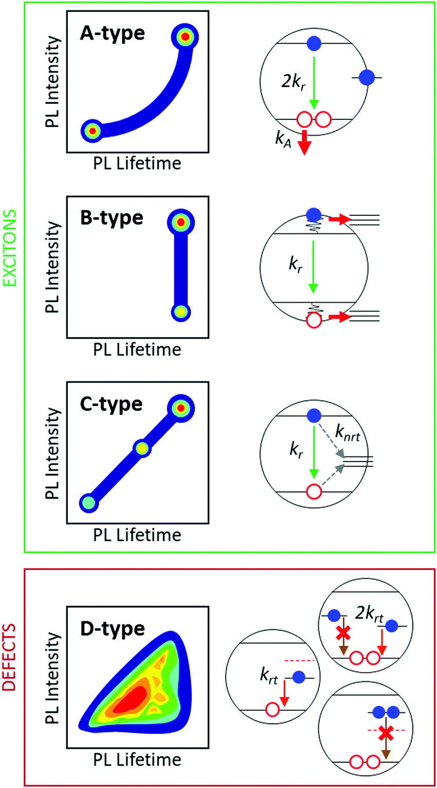 | ||
| Fig. 1 Illustrative representation of FLID maps showing the different types of blinking that are specific to different physical mechanisms. A-type: conventional carrier trapping with the following Auger relaxations. B-type: hot carriers trapping followed by radiative relaxation through core states (sometimes referred as B-HC blinking12,13). C-type: band-edge carriers trapping by time-dependent opening and closing of short living trap centres providing fast nonradiative channel for excitons (sometimes referred as BC-blinking12). Emission in the A, B and C-type blinking only originates only from the excitonic channel. Trapping centres associated with surface states are responsible here for modulating excitonic relaxation behaviour. The D-type: blinking pattern that is separate from the excitonic channel and requires radiative relaxation through defect states. It is characterized by broad dispersion of both PL intensity and lifetime. According to the proposed models, it can be formed by several defect-mediated mechanisms. One is the fast switching between emissive and non-emissive behaviour of single defect centre. Second is independent trapping of excited electrons by either radiative or nonradiative centres. | ||
In this work we focus our attention on ternary QDs belonging to the AIBIIIXVI2 system (where A = Cu, Ag, B = Al, Ga, In and X = O, S, Se, Te), in which intrinsic point defects determine their electrical and optical properties.21 One of the most recognizable representatives of this group is gallium doped copper-indium selenide (CuIn1−xGaxSe2, CIGS). Its successful photovoltaic applications results from effective absorption,22 bandgap tunability23 and very good electrical conductivity even for polycrystalline thin films.24 Meanwhile two different materials, namely CuInS2 (CIS) and AgInS2 (AIS), have attracted much attention as potential cadmium-free probes for bioimaging.25–27 Calculations done by the group of Alex Zunger contributed significantly to the understanding of the defect physics of the AIBIIIXVI2 semiconductors. It was found that good performance of polycrystalline samples results most likely from mutual neutralisation of charged, defect-forming clusters (e.g. 2VCu− + InCu2+).21 It is also believed that high tolerance to the off-stoichiometry and stabilization of various non-stoichiometric phases, e.g. AIBIII5XVI8, AIBIII3XVI5, AI3BIII5XVI9, is a direct consequence of defect clustering and their mutual interactions.28 The presence of such defects in nanocrystals allows one to tune their properties like emission, absorption or quantum yield not only by the quantum confinement effect, but also by intentional composition change.17,29 It is well-known that intrinsic defect mediated transitions are largely responsible for photoluminescence in CIS and AIS QDs.17,30–38 They are responsible for peculiar properties like the large Stokes-shifts, broadband emission, long decay times or temporal red-shift of the PL maximum. Very recently, narrow photoluminescence was achieved in AIS QDs after coating of the AIS core with InSx or GaSx amorphous shells39 or by post-synthetic exchange of thiolate-ligands (DDT) to phosphine-ligands (TOP).40 However, the existence of defect-related luminescence could not be completely eliminated.
It is therefore clear that application of models for which exciton recombination is the only emissive channel and defect related processes only act as time-variable modulator to the range of ternary and multinary QDs is not justified and will lead to spurious results. These models (A-, B- and C-Type) are not able to frame simultaneous optical processes, leading to the emission of photons at different rates and energies. Therefore, it seems reasonable to consider models for which either excitonic or defect-mediated transitions are possible. This leads to an issue with blinking patterns formed by purely defect assisted radiative relaxations and arising implications for the excitonic relaxation processes.
This problem has been taken up in this paper, both from the theoretical and experimental side. The AIS and CIS QDs were chosen as the experimental reference models expressing radiative defect assisted relaxations with a heavily supressed excitonic channel. These QDs were carefully examined experimentally in terms of intensity-lifetime correlations with strong emphasis on differences from those observed for binary QDs. Based on the defect physics of the AIBIIIXVI2 compounds, three different theoretical models are discussed. To maintain required simplicity, we have decided to investigate only the most probable optical processes. These include kinetics related to time correlated changes in the charge state of a single defect and radiative transitions by two different types of defect states. In all these models, both excitonic and defect-mediated transitions can occur simultaneously. However it is worthwhile to note that any excitonic transitions will be strongly correlated with the defects-related channel. All the schemes were simulated within the Kinetic Monte Carlo method. The manuscript is organized as follows: The time-resolved PL traces taken experimentally for individual CIS and AIS QDs are presented together with their intensity-lifetime correlation distribution. The results are discussed compared to previous reports on blinking from ternary semiconductor nanocrystals and their binary analogues.
Then, we propose three different relaxation schemes in individual QDs whose major task is to cover most of the kinetic processes that occur in CIS and AIS QDs. The proposed models include (i) radiative recombination of a trapped carriers, (ii) correlated trapping of electrons to previously filled trap states or (iii) uncorrelated trapping of electrons in two trap states of different nature.
Models are carefully analysed for a process's lifetime sets, covering a wide range from nano- to milliseconds. FLID maps are presented for a chosen group of parameters and discussed in terms of experimental and literature results.
Results and discussion
Experimental results
Representative photoluminescence traces taken for single CuInS2 and AgInS2 QDs are shown in Fig. 2a and c (additional results in Fig. S1 and S2, ESI†).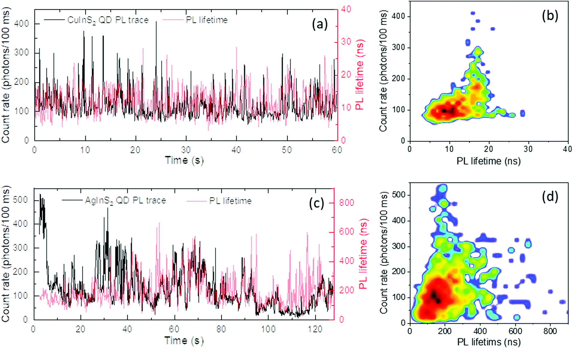 | ||
| Fig. 2 Representative PL traces taken experimentally for single (a) CuInS2 and (c) AgInS2 QD. Photoluminescence traces (black lines) and lifetimes traces (red lines) are plotted with 100 ms bin. Both samples were characterized by relatively fast bleaching. No distinct switching between well-defined bright and dark states can be observed. The emission is sparse in a form of short-living signals with non-uniform distribution of intensities. The FLID colour maps calculated for both samples are shown in (b) and (d) respectively. The coloration represents the intensity of two-dimensional correlation: white(zero)-blue-green-yellow-orange-red(maximum). FLID maps are characterized by very broad dispersion of both PL intensities and PL lifetimes forming fan-like shape. Additional PL traces and FLID maps of individual AgInS2 and CuInS2 QDs are presented in Fig. S1 and S2, ESI.† | ||
Along with the PL traces, the temporal evolution of the PL lifetime parameter (τPL) has also been presented. The lifetime parameter was evaluated for each 100 ms binning time interval using the first-order decay law. Several characteristic features regarding the experimental data must be noted. Firstly, both samples indicate quite low photon emissivity, below 500 photons/100 ms. Typically for these samples, photons are rarely emitted, providing something resembling an inverted blinking pattern. It is clearly visible that ternary QDs spend most of their time in the OFF state, interrupted intermittently by sparse or bunched photon emission.
Similar patterns have also been reported in our previous work,41 as well as by other authors.42–46 It is specific for AIS QDs that switching between well pronounced ON and OFF levels is uncommon. PL traces of AIS QDs can be described as flickering with continuous distribution of intensities. This behaviour indicates that several recombination mechanisms contribute to the emission on a time scale much faster than the binning time. Switching between traces taken for CIS QDs seem to be more uniform when compared to those taken for AIS QDs. The dark state level for CIS QDs is usually higher than for AIS QDs, being settled at around 100 photons/100 ms, and it almost never drops close to the zero level. On the other hand, the AIS traces exhibit rather variable dark state levels, which may reach almost zero photon emission. Both types of QDs were prone to quite fast bleaching. Complete quenching of photon emission was frequently observed after several to a few tens of seconds. According to our experiments, this process was permanent, and no further PL emission recovery was noticed, indicating complete photo-damage of the emitters. Similar PL traces were also reported by other authors. However, previous reports on blinking of ternary QDs lack the analysis of mutual correlation of PL intensity and lifetime. Fluorescence lifetime intensity distribution (FLID) mapping is a useful tool to further analyse the mechanisms that govern the blinking dynamics of individual QDs based on the correlation between PL lifetime and intensity.11,12,14 Each point on the FLID map is defined by a collection of photons that were assigned a binning time interval. Naturally, these individual photon patterns are determined by a set of various processes i.e. P = 〈X0,XX,X+,X−,Dn,An…〉 that occurred during each binning time.47 Therefore, a FLID map depicts the distribution of the contractual/imaginary strength of the predominate processes belonging to the set P that could evolve during a chosen time interval. In general, such maps are defined for a given binning time and should be compared using this same interval. Identification of various processes based on FLID maps is associated with the fact that any optical process has its characteristic boundaries determined by process rates.
Representation in a two-dimensional PL intensity and PL lifetime space is therefore very convenient and helps one to resolve mechanisms as well as their transitional superposition. The FLID maps that correspond to the representative CIS and AIS traces have been shown in Fig. 2b and d. The most notable feature of these maps is their broad spectrum of transitional states which exist in firm contrast to the most widely discussed blinking mechanisms reported previously for II–VI QDs.11,12 For both CIS and AIS QDs, the FLID maps resemble an irregularly shaped form with many separated spots of low intensities. Similar broad FLID maps were recently reported by Rabouw et al. for core-only CIS and core–shell CIS/CdS QDs however without detailed explanation.46 It seems to be clear that such complex behaviour of PL lifetime intensity distribution cannot be described correctly by any of the well-established blinking models. Other excited state relaxation pathways that consider defect mediated transitions must therefore be taken into consideration. In this work we would like to discuss other relaxation schemes that may give rise to very broad distributions in the FLID maps and which are strictly related to defect transitions instead of the excitonic part.
Numerical simulations
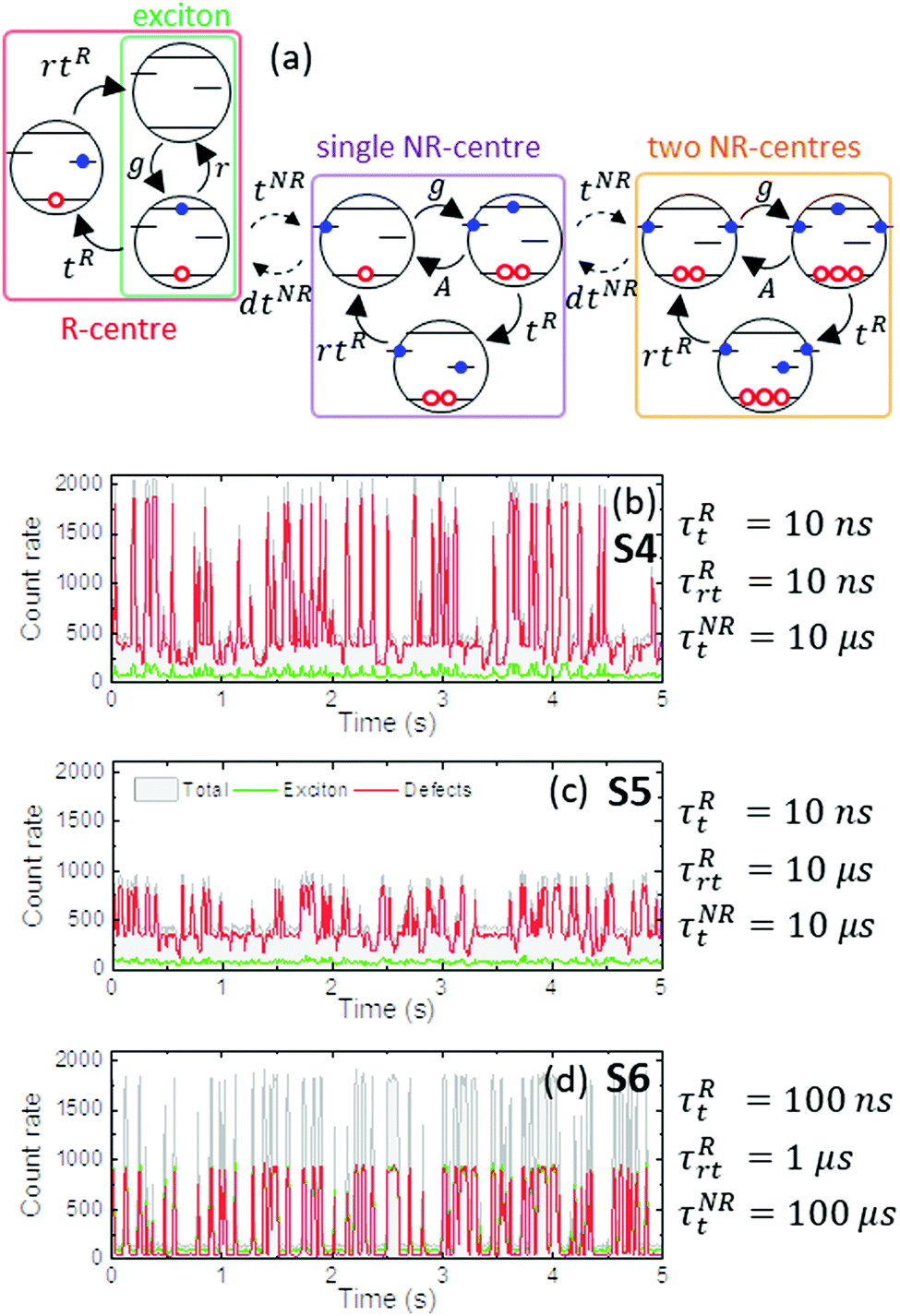
Simulation of kinetic processes occurring in single I–III–VI QD was performed numerically within the Kinetic Monte Carlo (KMC) method.48 An arbitrary QD is considered here as a simple two-level system, i.e., ground and excited state, with an additional trap centre that can bind excited carriers and provide a nonradiative relaxation path. In this work we propose three different relaxation schemes whose major task is to cover the major optical processes occurring in CIS and AIS QDs being responsible for broad spectrum at the FLID maps (Fig. 3). The proposed schemes mimic various electronic transitions while preserving their universal character. The first model assumed in this work is denoted as M1. In addition to the well-known charging model, the M1 scheme permits the radiative recombination of trapped electron from a defect state (Fig. 3). The emission from individual QD here is an interplay between simple, band-edge recombination and trapping events followed by trap-state radiative recombination. In the second model, denoted as M2, two electrons can be trapped in the same trap centre (Fig. 3). A second electron can be trapped by a centre filled previously with another electron. After trapping of a second electron, the nature of the trap changes from radiative to non-radiative. It results in long-lasting charging and quenching of luminescence. In the last model, named M3, two different types of trap centres (namely R-centres and NR-centres) are present in an individual QD (Fig. 3). Radiative recombination is allowed for R-centres, but not for NR-centres. An excited electron can be trapped independently by one of these traps. The temporal correlation imposed by sequential electron trapping is cancelled out. The rates of each electronic transitions are parametrized by rate constants kn = 1/τn, where τn is associated with the lifetime constant. A detailed description of the kinetic equations, parameters and numerical procedure for all considered models is given in ESI.†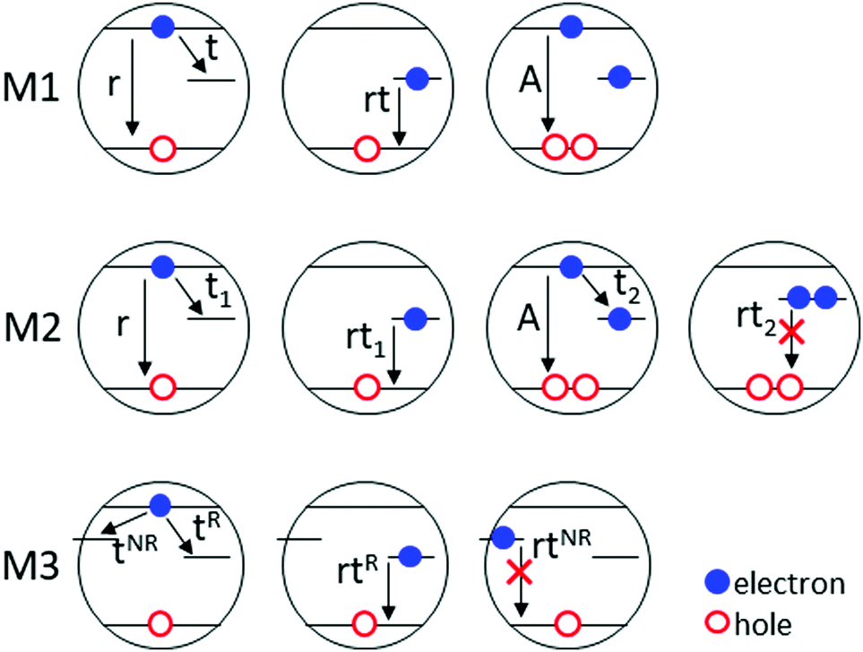 | ||
| Fig. 3 Schematic representation of the discussed models. M1: Radiative recombination of an trapped electron. Trap centres mediate in fast trapping (t) and radiative recombination (rt) processes. Defect emission is competitive to exciton recombination (r). Ratio of defect to excitonic emission is controlled by the trapping rate (kt) and the number of empty defect centres in a NC. M2: The change of the nature of defect centre's from emissive to non-emissive is time correlated. Thus change is assumed to occur when the second electron is trapped (t2) by previously filled trap state. Radiative recombination is allowed for a single charged defect state (rt1) but not for a double-charged state (rt2). M3: Independent trapping by distinct defect states of different kinds: radiative (tR) and nonradiative (tNR). The R-centres mediate in fast trapping and radiative recombination, while the NR-centres provide long-lasting charge blocking. | ||
Conventional charging model
Before further discussion of more complicated models, we want to refer to the main features of the conventional charging model.6,49 Blinking in the charging model originates from switching between two well-defined states i.e., bright (ON) state and dark (OFF) state. In the bright state, every generation process is followed by radiative excitonic recombination (g ⇄ r, Fig. 4a). The dark state emerges when one charge carrier (e.g. electron) is transferred to an external, long-lasting trap state. The remaining carrier (hole) provides internal charge off-balance that effectively interacts with an exciton and quenches the photoluminescence. Fast, nonradiative Auger processes dominate after generation during the dark state (g ⇄ A, Fig. 4a). The ON/OFF switching occurs due to trapping and detrapping processes (Fig. 4a). These processes need to be slow and occur once every few bins. Hence both bright and dark states are associated with distinct intensity levels observed on the PL trace (Fig. 4b). Slow trapping/detrapping rates are implied by the nature of the deep trap state localized outside of the QD's core. It is assumed that the trapping centres originate from surface defects or the surrounding matrix.5,6 When ON/OFF switching is faster than the binning time, it will occur multiple times within a single bin, resulting in continuous emission with intermediate intensity (Fig. S9 and S10, ESI†). | ||
| Fig. 4 (a) Graph representing cycles of optical processes in a conventional charging model. Bright state (green frame) consists of alternating generation (g) and exciton recombination (r) events. Transition to the dark state (black frame) takes place after trapping (t) of an electron to a deep trap state associated with the NC surface. In the dark state after every generation, emission is effectively quenched by rapid Auger (A) processes. Neutralization of the QD's core occur after detrapping (dt) via thermally activation or tunnelling processes. (b) Representative PL trace and (c) FLID map calculated for set of rates g = 2 × 10⁵, kr = 108, kA = 109, kt = 103, kdt = knrt = 10 [s−1]. Count rate in 1000 photons/10 ms. Since the trapping/detrapping processes are of low probability, a switching between two well-defined PL intensity levels can be seen. To areas observed in FLID map result from neutral exciton and charged trion recombination. | ||
Since the charging model is, in fact, limited to only two physical mechanisms, i.e. radiative exciton (krnp) and nonradiative Auger (kAnp)2 relaxation, it implies a power-like dispersion of the FLID distribution (Fig. 4c). Two boundary regions corresponding to 〈N·X0〉 and 〈N·X+〉 sets are well outlined on the FLID maps. The PL lifetime calculated for the bright state matches the assumed lifetime constant for exciton radiative recombination τPL = τr = 10 ns.
Although the charging model can be useful for some QDs, more complicated FLID correlations require one to reach for more complex schemes. The fundamental assumption of the charging model is that the only channel of emission from QD is through radiative exciton recombination. Hence its applicability to materials where emission originates mainly from defects is inadequate and may lead to spurious conclusions.
Model M1 – allowed radiative recombination from defect state
To mimic real optical processes in I–III–VI QDs, one need to consider at least two channels of radiative recombination, i.e. excitonic and defect mediated (Fig. 3). It is important to point out that trap states considered in the model M1 are of a different nature than the one simulated in the referenced charging model. For the charging model, trap states originated from the QD's surface or its surrounding matrix. They were characterized by slow trapping rate and prolonged time (∼100 ms) before carrier release. Here trap centres are associated with intrinsic point defects or defect clusters that are abundant in ternary semiconductors.21,28 Trapping and radiative recombination processes involving intrinsic defects should be associated with much shorter lifetimes comparable with radiative excitonic recombination.34,35,50,51 Therefore, total emission consists of two competing cycles of radiative relaxation (Fig. 5c). Excitonic emission is a cycle of alternating generation and recombination events (g ⇄ r), while trap state emission is a cycle of generation, trapping and radiative recombination from trap state (g → t → rt → g…). A quick release of the trapped carrier before radiative recombination eliminates Auger nonradiative processes. The trap state is cleared quickly (krt = 108–107 s−1) and cannot provide long-lasting charge imbalance before a second generation event (g ∼ 105 s−1). Therefore, a continuous bright state and a maximal total emission intensity without visible ON/OFF switching are observed (Fig. 5a, b and Fig. S11, ESI†). According to this model, an excited electron can recombine with only one hole, but it can be trapped by one of many empty traps. Hence, for equal rates of exciton recombination and trapping (kr = kt = 108 s−1), defect-mediated recombination is even more probable and is responsible for about 90% of total emitted photons (Fig. 5a). Lowering the trapping rate results in increased excitonic share in the total emission (Fig. 5b and Fig. S11, ESI,† for further details).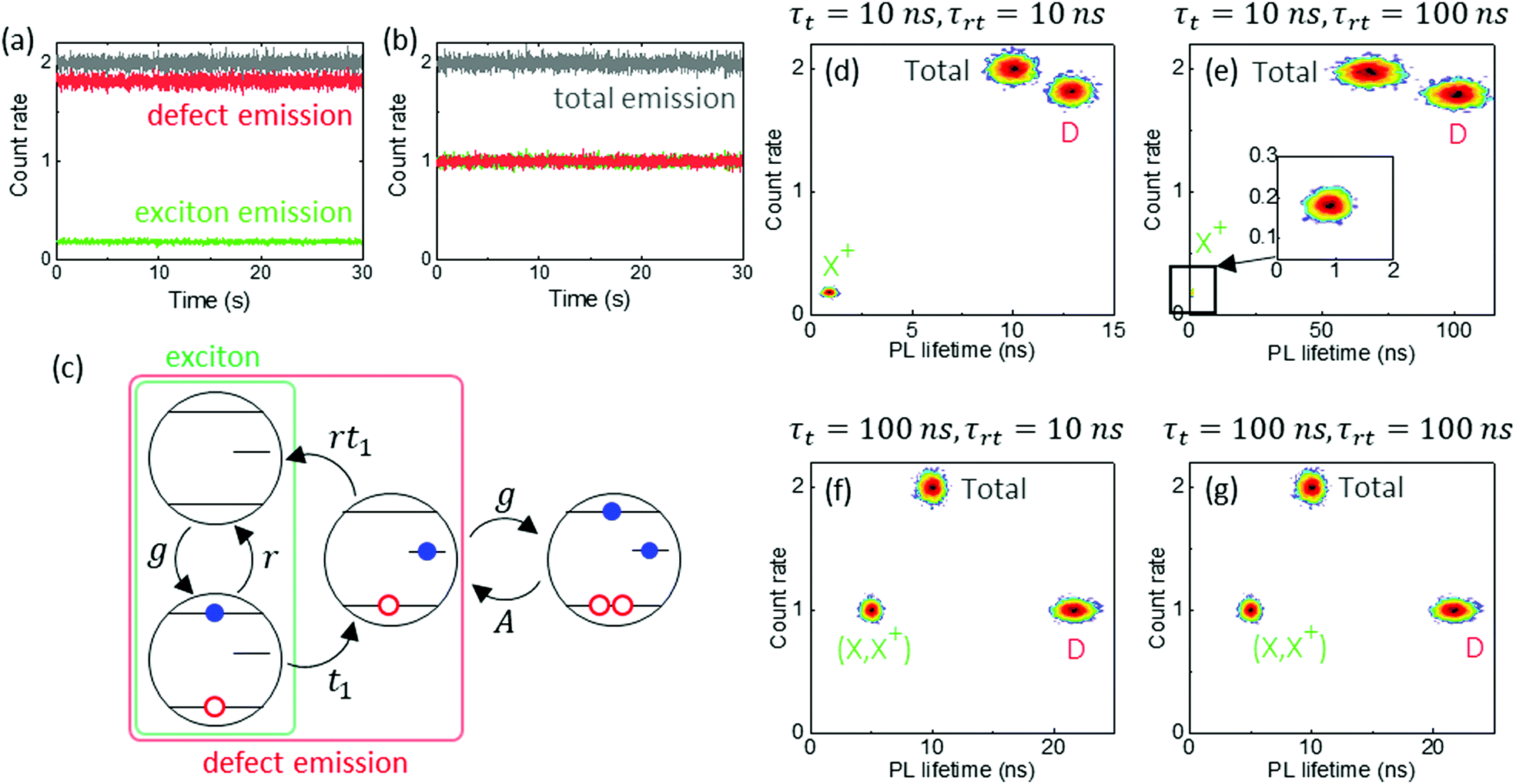 | ||
| Fig. 5 Representative PL traces calculated for trapping rates (a) kt = 108 and (b) kt = 107 [s−1]. Exciton and defect radiative recombination rate were kr = krt = 108 s−1, other rates the same as in Fig. 4 caption. Exciton, defect and total emission were coloured in green, red and grey respectively. Continuous emission without any dark state formation was obtained. Considering identical exciton recombination and trapping rates (a) defect emission dominates due to number of empty traps (stot = 10). (c) Graph representing cycles of processes most occurring in M1 model. Excitonic (green frame) and defect emission (red frame) are two competing cycle that start with the same generation event. (d–g) Representative FLID maps calculated within M1 model for every combination of (τt, τrt ∈ (10 ns, 100 ns)). Count rate unit is 1000 photons/10 ms. Excitonic (X), defect (D) and total emission were presented separately on every map. Total emission intensity is a sum of emission intensities from separate channels. Total PL lifetime is averaged over values for excitonic and defect PL lifetimes. | ||
Another feature of this model is the importance of photon distinction during FLID analysis. PL lifetime derived from total photons emitted in a particular bin results in an averaged value. The averaged PL lifetime may be one order of magnitude lower than the defect emission lifetime, even when it dominates the total emission (Fig. 5d–g). Since several different sources may participate in the total emission, information about their relaxation lifetimes and the related nature of the defects is lost in the averaging process. Therefore, considering only total emission during FLID correlation analysis, one may misidentify the nature of the emission. The experimental distinction of photons emitted from different channels may be difficult depending on the sample and experimental setup. However, such experiments were recently reported.52,53 Although the presented model M1 cannot reproduce blinking behaviour, it is essential to understand mutual dependencies between excitonic and defect related emission channels. The restoration of blinking is possible only when long lasting charge blocking can be provided, i.e. when the M1 model reduces to simple charging model. This result is expected, as blinking by the excitonic channel must result from charge blockade, because excitons are prone to charging. The situation is completely different for relaxation through defects, where Auger relaxations are not important. The occurrence of blinking in the defect-related channel must therefore fulfil other conditions.
This is discussed in detail for models M2 and M3, framing a wider range of possible transitions.
Model M2 – time correlated trapping of more than one electron at a single centre
This scheme is intended to reflect physical changes of a defect's charge state and correlated transition energy levels. Regarding I–III–VI compounds, this applies to a wide range of point defects as well as interacting (charged) and non-interacting (neutral) defect clusters. Transition energies for various defects are typically below 0.7 eV,24 but more importantly, a defect's charging changes its character. Such changes are typically quite strong and can manifest themselves as a complete reversal of a defect's type, e.g. from donor to acceptor-like. This fact has been enclosed in the M2 model. It is worthwhile to point out that the M2 model is not intended to accurately reflect the kinetics occurring at each type of defect. Its task is to capture the correlation resulting from the sequencing of events (trapping of one or two electrons) and the resulting implications for excitonic and non-excitonic blinking. The most important implications resulting from defect charging have been used to form the M2 transition scheme. The change in the defect's nature is therefore strongly assigned to a well-defined physical mechanism. According to the M2 model, an emissive defect can release a trapped electron in a radiative recombination process. The change to a non-emissive defect state is expected to be characterized by low-probability along with long-lasting charging due to slow detrapping rates. Some conceptual similarity related to activity switching can be found between the M2 model and the C-type blinking path. In the C-type blinking, the bright state is assumed to occur when nonradiative recombination centres are inactive. Their random activation followed by fast nonradiative decay channel results in PL flickering.10 It should be emphasized, that C-type pathway affects only excitons. Random switching of non-radiation processes between active/inactive state is only a factor modulating the radiative transitions from the exciton. The microscopic origin of such active/inactive random switching is still not fully understood.12Sharma et al. presented valuable experimental premises for the defective origin of photons emitted from single AIS-ZnS QDs.42 According to their model, it was conceptualized that two donor levels (D1 – non-radiative of higher energy, D2 – bright with lower energy) are involved in radiative relaxation. Their model assumes that only the D2 level may be switched between radiative and non-radiative state.
Contrary to D1, level D2 may be populated directly or by non-radiative relaxation from band-edge states. In a typical example, it is assumed that optical excitation is followed by a non-radiative relaxation to a D2 level. Further relaxation from the D2 level is responsible for emission of low energy photons. It is also assumed that the D2 level may become a long-lived trap. For such a situation, the D1 level takes over the role relaxing non-radiatively. Moreover, unlike D2 the D1 cannot be populated directly by the excitation source. The switching of the D2 level from radiative to non-radiative was assigned by authors to surface states. Lany and Zunger have described the formation of deep electron traps on defect clusters in ternary chalcopyrites like CuInSe2 and CuGeSe2.54,55 Intrinsic ionized donors (InCu2+ and GaCu2+) can be transformed into lattice-relaxed, deep DX centre by capturing two electrons (InCu2+ + 2e → InDX0).54 It was also shown that divacancy complexes (VSe − VCu)q can change their type from shallow donor (q = +1) to shallow acceptor (q = −1) configuration and vice versa by persistent carrier capture or emission.55 Although it was originally proposed to explain experimental behaviour of polycrystalline CIGS samples, such kind of defect centres and clusters can strongly manifest their activity in the optical spectroscopy of AIS and CIS QDs. Here we propose that charge state changes on individual point defects as well as in defect clusters may be responsible for dark state formation due to a carrier's prolonged stay in a trap at the given charge state (Fig. 3). Therefore, the same defect centre (or cluster) may be responsible for both emission and dark state formation, depending on its charge state. It is important to note that internal kinetics within the cluster is more complicated and would require separate schemes for various cluster types. Therefore, we have decided to limit our considerations to the most generalized case. This is justified by the fact that the most important physics standing behind the electronic transitions are preserved, and the obtained results are more intuitive and better understood. Model M2 assumes trapping of more than one excited electron by a modelled trap centre (Fig. 3). A single-charged trap state is opened for radiative relaxation in a similar way as it was for model M1. Trapping of a second electron by previously filled trap switches it to a long-lasting, non-emissive state. All detrapping and recombination rates of double-charged defects were set to slow values (τdt/nrt/rt = 100 ms) to provide prolonged charging and the possibility of effective emission quenching. Processes involving singly or doubly occupied defects are denoted with subscripts 1 and 2 respectively (Fig. S5, ESI,† for detailed description). Calculations in model M2 were done for a wider range of single (τt1) and double (τt2) electron trapping rates and single-charged defect radiative recombination rate (τrt1).
Every combination of rates (τt1,τrt1,τt2) was considered here to examine mutual dependencies between these processes (Fig. S13–S15, ESI,† and discussion there). In such an approach, it is possible to find trends in the kinetics of the optical processes resulting from an interplay between trapping and recombination events. Trapping of a second electron (and thus switching to the dark state) may be done only by traps already filled with one electron, which are also responsible for defect-related emission. Therefore, dark state formation and defect emission are two mutually correlated processes. Formation of the dark state in the M2 model depends on two factors. The first is the availability of single-charged traps that is directly proportional to first electron trapping rate (kt1) and inversely proportional to the defect radiative recombination rate (krt1). The second factor is the rate of second electron trapping (kt2).
For the second electron trapping to occur, a single-charged trap cannot recombine radiatively until another electron–hole pair is generated. Thus, a slow recombination rate (τrt1 = 1–10 μs, krt1 = 105–106 s−1) favours the possibility to leave the cycle of defect emission (g → t1 → rt1, red frame in Fig. 6a). A second excited electron can either be trapped by a single-charged trap or recombine within the nonradiative Auger process, thus returning to the defect emission cycle (Fig. 6a, middle part). When the second electron trapping is slow (τt2 ≥ 1 μs, kt2 ≤ 106 s−1), it cannot compete with the efficient nonradiative Auger recombination (kA = 109 s−1). Blinking behaviour cannot be achieved, and the M2 model reduces to the previous M1 scheme with continuous emission (Fig. S13–S15, ESI†). When a second electron is finally trapped, a double-charged defect provides sustained charge off-balance, and the QD is in the dark state (blue frame in Fig. 6a). Quenching of excitonic emission is even more effective, due to quadratic scaling of the Auger process rate with the number of free holes (kAnp2). Excited electrons can still be trapped by remaining empty traps and recombine radiatively. However, this emission should be characterized by about three times shorter lifetime due to the abundance of holes that can participate in defect-mediated recombination (blue frame in Fig. 6a). Detrapping processes from double-charged defects are of low probability (kdt/nrt = 101 s−1). However, due to the count of carriers that could participate in detrapping processes (2 electrons and 2 holes), they can happen more often than in the reference charging model. Therefore, the dark state in the M2 model is, in fact, less stable than in the charging model, and ON/OFF switching can occur several times within a single binning period (10 ms).
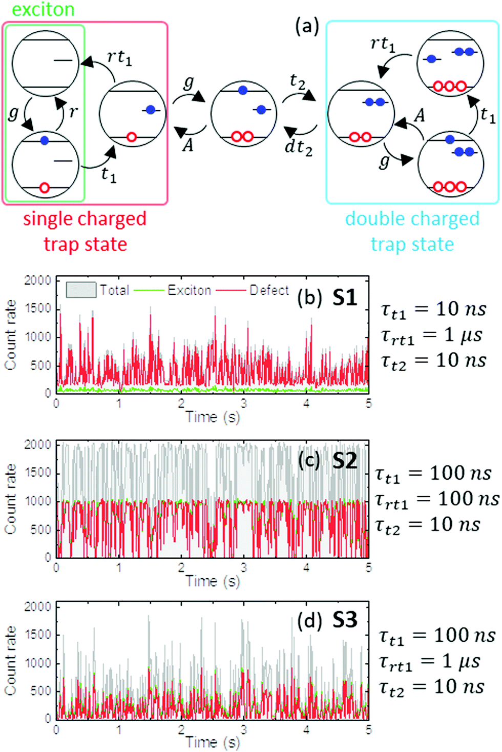 | ||
| Fig. 6 (a) Graph representing cycles of optical processes most occurring in M2 model. Excitonic (green frame) and defect (red frame) emissions are competing cycles after generation. When defect PL lifetime is prolonged, second electron can be excited and trapped by the same trap state (middle part). Defect centre changes its nature to non-emissive then (blue frame). Double-charged trap state provides long-lasting charge blockade and effective quenching of exciton emission by Auger processes. Further trapping by another empty trap states and defect-related emission is still possible. (b–d) PL traces simulated for three representative calculation sets (b) S1, (c) S2 and (d) S3 within M2 model. Chosen values of (τt1,τrt1,τt2) parameters are given. See ESI,† for calculation details. For sets S2 and S3 (c and d) both exciton and defect emission count rate are 50% of total emission intensity. Hence on the graph, exciton emission (green line) is covered by defect emission (red line). Count rate given in photons/10 ms. | ||
Three calculation sets (namely S1, S2, S3) were chosen as representative examples of blinking behaviour simulated within the M2 model. PL traces (Fig. 6b–d) and FLID maps (Fig. 7) were obtained separately for exciton, defect and total emission.
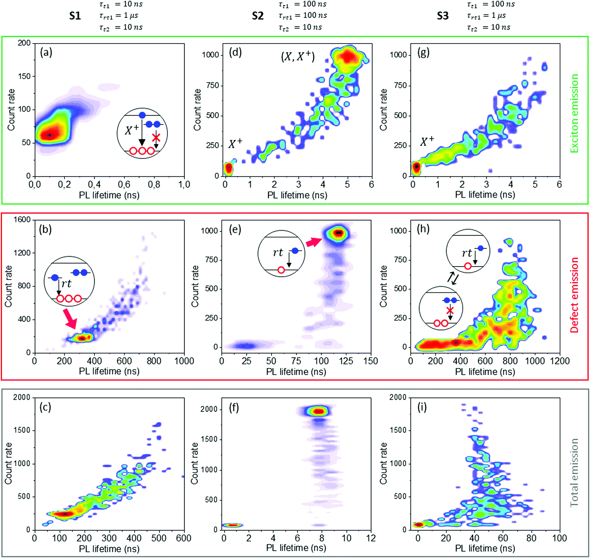 | ||
| Fig. 7 Representative FLID maps obtained for KMC simulations performed for the M2 scheme within three sets of (τt1,τrt1,τt2) parameters S1 (a–c), S2 (d–f) and S3 (g–i). The exciton emission is shown in the top pane (green frame), the defect emission in the middle pane (red frame) and the total emission in the bottom pane (grey frame). Count rate given in photons/10 ms. Broad dispersion of both PL intensity and PL lifetime is a result of multiple switching of defect centre between emissive (single charged) and non-emissive (double charged) state. | ||
In set S1, both trapping processes are fast (kt1 = kt2 = 108 s−1). Efficient trapping of excited electrons significantly supresses the exciton recombination cycle (Fig. 6b). Residual excitonic emission stays below 5% of the maximum total intensity with PL lifetime below 0.5 ns (Fig. 7a). Due to the prolonged stay of an electron in a single-charged trap state before emission (τrt1 = 1 μs) and fast trapping of second electron, the simulated QD often enters the dark state cycle (blue frame in Fig. 6a). Hence most of the photons emitted from defect are characterised with PL lifetimes ca. three-times shorter than the assumed 1 μs (Fig. 7b). This shows that defect-emission occurs mainly in the presence of another defect in the double-charged state.
In the S2 calculation set, the first electron trapping rate is slower by one order of magnitude (kt1 = 107 s−1). It increased the participation of exciton recombination in the total emission up to 50%. Also, radiative recombination from defects is assumed to be 10 times faster than in the previous set (τrt1 = 100 ns). It results in a lower availability of single-charged trap states and thus a lower chance for the dark state to occur. Both excitonic and defect emission can reach a maximum intensity of 1000 photons per bin. Dark states are in the form of short-living but dense drops of emission intensity (Fig. 6c). Two distinct maxima on FLID maps can be seen for both types of emission (Fig. 7d and e). Longer-lifetime and high-intensity maximum are associated with an uncharged bright state. Shorter-lifetime, low-intensity area results from residual emission in short-lived dark states. Moreover, the bright-state maximum on the defect emission FLID map (Fig. 7e) is vertically distributed to the level of zero photons with almost no change in PL lifetime, similar as reported by Galland et al.11 After detrapping of one electron from a double-charged trap, the remaining trapped electron may still recombine radiatively with its typical lifetime.
The PL trace of the S3 calculation set has the same characteristics as the S1 set, i.e. dense emission peaks separated by short-living dark states (Fig. 6d). Hence the analysis of the FLID maps is necessary here for proper understanding of the kinetics of the observed optical processes. First, the electron trapping rate is the same as for the S2 set (kt1 = 107 s−1), while the lifetime of the trapped electron before radiative recombination is prolonged, similar to the S1 set (τrt1 = 1 μs). The effective rate of dark state formation stays between two former cases. Excitonic recombination is decreased and no emission from neutral excitons can be observed (Fig. 7g). Interestingly, the FLID map of defect-emission in this set shows very broad dispersion of both PL lifetime and PL intensity (Fig. 7h). It results from fast switching between single- and double-charged defect states in the binning period. A distinct dark state with zero-photon intensity can be obtained only when charging lasts for at least the whole bin duration (10 ms). When charging lasts only for less than a full binning period, only some part of the total emission intensity can be quenched. The PL lifetime of the defect emission in the presence of another double-charged trap is shorter than undisturbed defect recombination. Also, the PL lifetime is averaged over all photons emitted in a particular bin. While ON/OFF switching may occur several times in a bin, it results in a broad dispersion of derived PL lifetimes.
Considering total emission only, the shape of FLID maps strongly reflect the nature of defect emission (Fig. 7c, f and i). However, the inclusion of short-lifetime excitonic emission has significantly lowered the total PL lifetime compared to defect emission lifetime. This shows that the analysis of averaged total emission could hinder a proper understanding of excited state relaxation in complex materials. The distinction of photons emitted from different sources was crucial to understand the influence of correlated single to double electron trapping on the formation of the dark state in ternary QDs.
Correlation of dark state formation with defect emission allows one to obtain broad dispersion of both PL lifetimes and intensities due to fast switching between single and double-charged defect states.
Model M3 – uncorrelated trapping by distinct defect sites with different nature – emissive and non-emissive
The last model (M3) described in this work is devoted to two distinct trap centres of different nature. Each of them can trap excited electrons independently. An important feature is that both traps are independent, and no temporal correlation is provided. The first type of traps, denoted as R-centres (superscript R), mediate in the radiative recombination process like the previous M1 model. The R-centres may be associated with intrinsic point defects or clusters, as discussed above. The second type are nonradiative traps denoted as NR-centres (superscript NR). The NR-centres are characterized with a low effective detrapping rate, and they provide long-lasting charge blocking.The NR-centres may be associated with surface-related defects, that can coexist with intrinsic point defects. Therefore, excited state relaxation depends on two competing independent trapping processes. Numerical simulations of the M3 model were carried out for a wide range of both centre trapping rates (τRt and τNRt) and emissive centre radiative recombination rate (τRrt). Every combination of rates (τRt,τRrt,τNRt) was considered to examine trends in excited state relaxation kinetics that result from two independent trapping processes (Fig. S16–S18, ESI,† and discussion there). Both radiative channels, i.e. excitonic and defects-mediated, are taken into consideration.
Although trapping by two different types of defects is fully independent in the following model, it begins from the same generation process. An excited electron may either recombine with a free hole (g → r, green frame in Fig. 8a), it may be trapped by an emissive centre (g → tR → rtR, red frame in Fig. 8a), or it may be trapped by a nonradiative centre, providing long-lasting charge off-balance (g → tNR, purple frame in Fig. 8a). Excitonic recombination and two kinds of trapping centres compete to “utilize” the excited electron. Transfers of an excited electron to/from the nonradiative centre are of low probability and happen once every few bins. Long-lasting charge blocking results in effective quenching of PL and distinct dark state formation. However, defect-mediated emission is not affected by Auger processes in the same way as the excitonic emission. For a very fast trapping rate, radiative centres may still effectively trap electrons and emit (purple frame in Fig. 8a). Therefore, the dark state should be associated with the residual defect emission, whose intensity depends on the trapping rate. It also should be characterized by shorter PL lifetimes, due to redundant free holes that could recombine with trapped electron. Due to the long stay of an electron in a nonradiative centre, it is possible that two electrons will be simultaneously trapped by two nonradiative centres (orange frame in Fig. 8a). It would result in a further drop in residual defect emission intensity, due to the increased importance of the Auger processes that scale quadratically with the number of free holes. As with the previous M2 model, three calculation sets (namely S4, S5, S6) were chosen as representative examples of QD PL intermittency simulated within the M3 model. PL traces (Fig. 8b–d) and FLID maps (Fig. 9) were obtained separately for exciton, defect and total emission. Both S4 and S5 calculation sets are characterized by fast trapping to R-centres (τRt = 10 ns). Hence, residual defect emission in the dark state can reach 25% of the total maximum intensity (Fig. 8b and c). Excitonic emission is significantly suppressed to a value below 10% of the total emitted intensity with lifetime below 1 ns (Fig. 9a and d). Two different levels of dark state are clearly visible on PL traces (Fig. 8b and c). A secondary drop in emission intensity results from another NR-trapping, before the previous NR-centre was released. Additional unbalanced charge also influences the PL lifetime of defect emission. Three distinct areas associated with unperturbed, single-charged and double-charged defect emission are visible on FLID maps (Fig. 9b and e). Every single unbalanced positive charge causes a significant drop in the PL intensity as well as PL lifetime. Defect emission in set S4 originates from a single R-centre, which can quickly trap and release an electron (τRt = τRrt = 10 ns, Fig. 9b). However, due to the assumed prolonged occupation of R-centres in set S5 (τRrt = 10 μs), several centres may emit at once (Fig. 9e). Trapping in the last calculation set S6 is slower by one order of magnitude for both kinds of traps. Slower trapping allows the more efficient excitonic recombination, which now counts for half of the total emission (Fig. 8d) with slightly shortened PL lifetime (Fig. 9g). Slower trapping by R-centres reduces the residual dark state emission below 5% of the total emitted intensity. Also, no influence from several NR-traps can be observed. FLID maps of both excitonic and defect emission show two characteristic areas (Fig. 9g and h): one is associated with uncharged emission in the bright state, and a second is associated with the dark state. The shape of the total emission FLID maps is strongly imposed by defect-related emission (Fig. 9c, f and i). The impact of excitonic emission is expressed only by shortening of the total PL lifetimes.
 | ||
| Fig. 8 (a) Graph representing the cycles of optical processes most occurring in the M3 model. An excited electron can either recombine with free hole (green frame), by trapped by radiative centre (red frame) or be trapped by the nonradiative centre (purple frame). The R-centres mediate in defect emission, while NR-centres provide long-lasting charging. When the charge is blocked in the NR-centre, exciton emission is effectively quenched. Trapping by R-centres is still possible. It results in residual non-zero defect-emission in dark state. Filling of multiple NR-centres (orange frame) results in more rapid quenching and further drop of residual emission. Trapping and detrapping to NR-centres are of low probabilities. (b–d) PL traces simulated for three representative calculation sets (b) S4, (c) S5 and (d) S6 within M3 model. Chosen values of (τRt,τRrt,τNRt) parameters are given. See ESI,† for calculation details. For sets S6 (d) both exciton and defect emission count rate are 50% of total emission intensity. On the graph exciton emission (green line) is covered by defect emission (red line). Count rate given in photons/10 ms. | ||
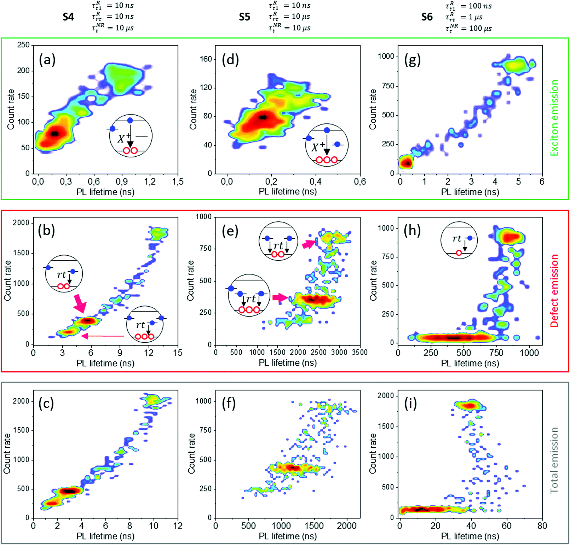 | ||
| Fig. 9 Representative FLID maps obtained for KMC simulations performed for the scheme M3 within three sets of (τRt,τRrt,τNRt) parameters S4 (a–c), S5 (d–f) and S6 (g–i). The exciton emission is shown in the top pane (green frame), the defect emission in the middle pane (red frame) and the total emission in bottom pane (grey frame). Count rate given in photons/10 ms. Well defined levels of PL intensity are correlated with the number of occupied nonradiative centres. | ||
Conclusions
This work aimed to investigate, both experimentally and theoretically, a new type of blinking pattern, which we call here the D-type. This D-Type blinking results from non-excitonic, defect assisted radiative transitions.It is shown that radiative relaxation through defect states may also result in a blinking pattern. Due to different kinetics, this pattern is completely different from those known for the excitonic relaxation. Also, different conditions must be met to observe blinking from defects. We have already recognized only two schemes. Both are collected in Table 1 and compared with the one known for excitonic blinking pathways.
| Conditions required to observe blinking | |
|---|---|
| Radiative from excitons | Radiative from defects |
| + Charge imbalance | + Correlation (M2) |
| Exciton is sensitive to uncompensated internal charge. Different blinking types rely on temporal evolution of non-radiative processes which are modulated by various trapping schemes. | A process must wait for completion of another. |
| Currently known schemes: | The M2 model implementation: Change in the charge state. One state is radiative another one is not. Radiative process may occur only after return to lover charge state. |
| + Competition (M3) | |
| A-Type: conventional carrier trapping with following Auger relaxations | Trapping process concur with non-radiative relaxation. |
| B-Type: hot carriers trapping followed by radiative relaxation through core states | The M3 model implementation: When one nonradiative-type trap is filled, after second generation process, excited electron/hole competes with capture by defect and following radiative process or fast non-radiative relaxation. |
| C-Type: band-edge carriers trapping by time-dependent opening and closing of short living trap centres providing fast nonradiative channel for excitons | |
The first condition involves correlation of events (model M2), and the second one is related to competition (model M3) with other, faster processes. The implications of our research prove that blinking is a very universal process that always occurs in the presence of a certain “blockage”. This “blockage” may be of various nature. In the case of an exciton, the blockage is formed by the uncompensated charge. On the other hand, for relaxation by defects, it may be the temporal correlation as well as competition.
The D-type blinking was observed experimentally for AgInS2 and CuInS2 QDs, which are well-known from effective defects assisted emission. Experimental spectra taken for single AIS and CIS QDs revealed that their blinking character is highly divergent from any currently reported blinking type. Fluorescence intensity-lifetime correlations showed very broad dispersions of the PL lifetimes and PL intensities. Three up-to-date mechanisms of blinking, namely A, B and C-type, failed in explanation of these patterns. It is well rationalized as long as all of them is centred around the excitonic emission. These three mechanisms consider exciton recombination as the only pathway for photon emission from a QD. For these models the dark state is always formed as a result of exciton recombination quenching. Although this assumption is well justified for II-VI compounds, it is not completely adaptable for ternary semiconductors, whose electrical and optical properties are implicated by their rich nature of native defects.
We have proposed three theoretical models suitable for better understanding of both emission and dark state formation in ternary QDs, for which exciton recombination is not the main source of emission. In this work we sought to symmetrize different relaxation pathways and shift the weight from the excitonic channel toward an equally legitimate defect relaxation. Kinetic Monte Carlo simulations were performed for a wide range of trapping and recombination rates (as well as their combinations) to understand mutual dependencies between different recombination paths.
The first model (M1) described competitive emission from either excitons or intrinsic defects without long lasting charging of the QD. The dark state could not be obtained, since radiative defect centres could not provide charge blocking and effective PL quenching.
Two possibilities for dark state formation were considered in models M2 and M3. In the model M2, it was assumed that the same defect centres may participate in both emission and dark state formation. The dark state emerges, when the emissive defect centre changes its nature to non-emissive. Such a change may originate from the capture of two carriers by a single defect centre. This change is always correlated with previous trapping and may not occur in any other way. It forms a metastable configuration with prolonged lifetime before the recombination. We have found that such switching may occur multiple times within a single binning period. This temporal correlation results in a peculiar PL trace that has the form of a dense comb of short peaks. This bunch-like emission spans over the wide range of intensities, and no distinct low-intensity dark state is observed. The strong influence of unbalanced charge on defect-emission results in a broad range of PL lifetimes. As a result, a very broad dispersion of both PL intensity and PL lifetimes is observed in FLID maps which stays in very good agreement with observed experimental data.
Model M3 assumed the existence of two different and uncorrelated defect centres, i.e. radiative and non-radiative ones. Radiative centres mediate in defect emission, while non-radiative centres can capture excited carriers and effectively block them. Because nonradiative centres provide long-lasting charge blocking, dark states in model M3 are stable and can last for several bins, unlike in the M2 model. However, the dark state is characterized by distinct non-zero, defect emission intensity. This residual emission originates from radiative centres, that are still active, while excitonic emission is q quenched by Auger processes. We have also observed similar, clearly notable non-zero emission in CuInS2 QDs (Fig. 2a). Since the M3 model didn’t provide fast switching between emissive and non-emissive states, distinct levels of PL intensity were observed on PL traces and FLID maps. These levels correlate well with the number of occupied nonradiative centres. PL lifetimes span an even wider range of values, however, a broad dispersion similar to the M2 model could not be obtained.
The analysis of simulated PL traces and FLID maps was done separately for the photons emitted from excitons, intrinsic defects and for total emission. The shape of the total emission FLID maps strongly reflected those observed for defect-state emission. However, total emission PL lifetime was significantly reduced by the influence of photons emitted from short-lived excitons. We believe that the separation of different emission channels during FLID analysis could be of great importance in the future findings of excited state relaxation kinetics in the samples where several emission channels are competitive in total emission.
This is a first step in properly understanding the very complex relaxation kinetics of ternary semiconductor QDs. This complexity is as a consequence of charge rebalancing in both separate point defects or defect clusters. However, we believe that the simplified kinetic models presented here are suitable to understand the main properties of ternary QDs observed at the single-particle level.
Conflicts of interest
There are no conflicts to declare.Acknowledgements
B. Cichy acknowledge financial support from the National Science Centre within the frame of SONATA BIS program (2018/30/E/ST3/00580).References
- W. E. Moerner and L. Kador, Phys. Rev. Lett., 1989, 62, 2535–2538 CrossRef CAS PubMed.
- M. Orrit and J. Bernard, Phys. Rev. Lett., 1990, 65, 2716–2719 CrossRef CAS PubMed.
- R. M. Dickson, A. B. Cubittt, R. Y. Tsient and W. E. Moerner, Nature, 1997, 388, 355–358 CrossRef CAS PubMed.
- L. Möckl and W. E. Moerner, J. Am. Chem. Soc., 2020, 142, 17828–17844 CrossRef PubMed.
- M. Nirmal, B. O. Dabbousi, M. G. Bawendi, J. J. Macklin, J. K. Trautman, T. D. Harris and L. E. Brus, Nature, 1996, 383, 802–804 CrossRef CAS.
- A. Efros and M. Rosen, Phys. Rev. Lett., 1997, 78, 1110–1113 CrossRef CAS.
- M. Kuno, D. P. Fromm, H. F. Hamann, A. Gallagher and D. J. Nesbitt, J. Chem. Phys., 2000, 112, 3117–3120 CrossRef CAS.
- M. Kuno, D. P. Fromm, S. T. Johnson, A. Gallagher and D. J. Nesbitt, Phys. Rev. B: Condens. Matter Mater. Phys., 2003, 67, 1–15 CrossRef.
- J. Tang and R. A. Marcus, J. Chem. Phys., 2005, 123, 054704 CrossRef PubMed.
- P. A. Frantsuzov, S. Volkán-Kacsó and B. Jankó, Phys. Rev. Lett., 2009, 103, 207402 CrossRef PubMed.
- C. Galland, Y. Ghosh, A. Steinbrück, M. Sykora, J. A. Hollingsworth, V. I. Klimov and H. Htoon, Nature, 2011, 479, 203–207 CrossRef CAS PubMed.
- G. Yuan, D. E. Gómez, N. Kirkwood, K. Boldt and P. Mulvaney, ACS Nano, 2018, 12, 3397–3405 CrossRef CAS PubMed.
- C. T. Trinh, D. N. Minh, K. J. Ahn, Y. Kang and K. G. Lee, Sci. Rep., 2020, 10, 1–8 CrossRef PubMed.
- T. Kim, S. Il Jung, S. Ham, H. Chung and D. Kim, Small, 2019, 15, 1–10 Search PubMed.
- F. T. Rabouw, F. V. Antolinez, R. Brechbühler and D. J. Norris, J. Phys. Chem. Lett., 2019, 10, 3732–3738 CrossRef CAS PubMed.
- T. Ahmed, S. Seth and A. Samanta, ACS Nano, 2019, 13, 13537–13544 CrossRef CAS PubMed.
- D. Moodelly, P. Kowalik, P. Bujak, A. Pron and P. Reiss, J. Mater. Chem. C, 2019, 7, 11665–11709 RSC.
- D. Aldakov, A. Lefrançois and P. Reiss, J. Mater. Chem. C, 2013, 1, 3756–3776 RSC.
- A. Sahu, M. S. Kang, A. Kompch, C. Notthoff, A. W. Wills, D. Deng, M. Winterer, C. D. Frisbie and D. J. Norris, Nano Lett., 2012, 12, 2587–2594 CrossRef CAS PubMed.
- M. Sharma, M. Olutas, A. Yeltik, Y. Kelestemur, A. Sharma, S. Delikanli, B. Guzelturk, K. Gungor, J. R. McBride and H. V. Demir, Chem. Mater., 2018, 30, 3265–3275 CrossRef CAS.
- S. Zhang, S. H. Wei, A. Zunger and H. Katayama-Yoshida, Phys. Rev. B: Condens. Matter Mater. Phys., 1998, 57, 9642–9656 CrossRef CAS.
- B. J. Stanbery, Crit. Rev. Solid State Mater. Sci., 2002, 27, 73–117 CrossRef CAS.
- H. Li, F. Qu, H. Luo, X. Niu, J. Chen, Y. Zhang, H. Yao, X. Jia, H. Gu and W. Wang, Results Phys., 2019, 12, 704–711 CrossRef.
- C. Rincón and R. Márquez, J. Phys. Chem. Solids, 1999, 60, 1865–1873 CrossRef.
- M. D. Regulacio, K. Y. Win, S. L. Lo, S. Y. Zhang, X. Zhang, S. Wang, M. Y. Han and Y. Zheng, Nanoscale, 2013, 5, 2322–2327 RSC.
- M. F. Foda, L. Huang, F. Shao and H.-Y. Han, ACS Appl. Mater. Interfaces, 2014, 6, 2011–2017 CrossRef CAS PubMed.
- B. Cichy, D. Wawrzynczyk, A. Bednarkiewicz, M. Samoc and W. Strek, Appl. Phys. Lett., 2013, 102, 243702 CrossRef.
- S. B. Zhang, S. H. Wei and A. Zunger, Phys. Rev. Lett., 1997, 78, 4059–4062 CrossRef CAS.
- O. Yarema, M. Yarema and V. Wood, Chem. Mater., 2018, 30, 1446–1461 CrossRef CAS.
- J. Krustok, J. Raudoja, M. Krunks, H. Mändar and H. Collan, J. Appl. Phys., 2000, 88, 205–209 CrossRef CAS.
- T. Chevallier, A. Benayad, G. Le Blevennec and F. Chandezon, Phys. Chem. Chem. Phys., 2017, 19, 2359–2363 RSC.
- Y. Hamanaka, T. Ogawa, M. Tsuzuki and T. Kuzuya, J. Phys. Chem. C, 2011, 115, 1786–1792 CrossRef CAS.
- A. S. Baimuratov, I. V. Martynenko, A. V. Baranov, A. V. Fedorov, I. D. Rukhlenko and S. Y. Kruchinin, J. Phys. Chem. C, 2019, 123, 16430–16438 CrossRef CAS.
- T. Chevallier, G. Le Blevennec and F. Chandezon, Nanoscale, 2016, 8, 7612–7620 RSC.
- N. S. Han, H. C. Yoon, S. Jeong, J. H. Oh, S. M. Park, Y. R. Do and J. K. Song, Nanoscale, 2017, 9, 10285–10291 RSC.
- A. S. Fuhr, H. J. Yun, N. S. Makarov, H. Li, H. McDaniel and V. I. Klimov, ACS Photonics, 2017, 4, 2425–2435 CrossRef CAS.
- D. H. Jara, K. G. Stamplecoskie and P. V. Kamat, J. Phys. Chem. Lett., 2016, 7, 1452–1459 CrossRef CAS PubMed.
- B. Cichy, A. Olejniczak, O. Bezkrovnyi, L. Kepinski and W. Strek, J. Alloys Compd., 2019, 798, 290–299 CrossRef CAS.
- T. Uematsu, K. Wajima, D. K. Sharma, S. Hirata, T. Yamamoto, T. Kameyama, M. Vacha, T. Torimoto and S. Kuwabata, NPG Asia Mater., 2018, 10, 713–726 CrossRef CAS.
- A. Hirase, Y. Hamanaka and T. Kuzuya, J. Phys. Chem. Lett., 2020, 11, 3969–3974 CrossRef CAS PubMed.
- B. Cichy, R. Rich, A. Olejniczak, Z. Gryczynski and W. Strek, Nanoscale, 2016, 8, 4151–4159 RSC.
- D. K. Sharma, S. Hirata, L. Bujak, V. Biju, T. Kameyama, M. Kishi, T. Torimoto and M. Vacha, Nanoscale, 2016, 8, 13687–13694 RSC.
- O. Stroyuk, F. Weigert, A. Raevskaya, F. Spranger, C. Würth, U. Resch-Genger, N. Gaponik and D. R. T. Zahn, J. Phys. Chem. C, 2019, 123, 2632–2641 CrossRef CAS.
- I. V. Martynenko, A. S. Baimuratov, F. Weigert, J. X. Soares, L. Dhamo, P. Nickl, I. Doerfel, J. Pauli, I. D. Rukhlenko, A. V. Baranov and U. Resch-Genger, Nano Res., 2019, 12, 1595–1603 CrossRef CAS.
- H. Zang, H. Li, N. S. Makarov, K. A. Velizhanin, K. Wu, Y.-S. Park and V. I. Klimov, Nano Lett., 2017, 17, 1787–1795 CrossRef CAS PubMed.
- S. O. M. Hinterding, M. J. J. Mangnus, P. T. Prins, H. J. Jöbsis, S. Busatto, D. Vanmaekelbergh, C. De Mello Donega and F. T. Rabouw, Nano Lett., 2021, 21, 658–665 CrossRef CAS PubMed.
- J. I. Pankove, Optical processes in semiconductors, Courier Corporation, 1975.
- J. C. Walter and G. T. Barkema, Phys. A, 2015, 418, 78–87 CrossRef.
- M. Ye and P. C. Searson, Phys. Rev. B: Condens. Matter Mater. Phys., 2011, 84, 125317 CrossRef PubMed.
- J. Sun, M. Ikezawa, X. Wang, P. Jing, H. Li, J. Zhao and Y. Masumoto, Phys. Chem. Chem. Phys., 2015, 17, 11981–11989 RSC.
- M. Sakamoto, K. Inoue, M. Okano, M. Saruyama, S. Kim, Y. G. So, K. Kimoto, Y. Kanemitsu and T. Teranishi, Nanoscale, 2016, 8, 9517–9520 RSC.
- S. O. M. Hinterding, B. B. V. Salzmann, S. J. W. Vonk, D. Vanmaekelbergh, B. M. Weckhuysen, E. M. Hutter and F. T. Rabouw, ACS Nano, 2021, 15, 7216–7225 CrossRef CAS PubMed.
- S. J. W. Vonk, B. A. J. Heemskerk, R. C. Keitel, S. O. M. Hinterding, J. J. Geuchies, A. J. Houtepen and F. T. Rabouw, Nano Lett., 2021, 21, 5760–5766 CrossRef CAS PubMed.
- S. Lany and A. Zunger, Phys. Rev. Lett., 2008, 100, 1–4 CrossRef PubMed.
- S. Lany and A. Zunger, J. Appl. Phys., 2006, 100, 113725 CrossRef.
Footnote |
| † Electronic supplementary information (ESI) available. See DOI: 10.1039/d1nh00424g |
| This journal is © The Royal Society of Chemistry 2022 |