
 Open Access Article
 This Open Access Article is licensed under a
 Creative Commons Attribution 3.0 Unported Licence
An ultrafast photodetector driven by interlayer exciton dissociation in a van der Waals heterostructure†
Edoardo
Lopriore‡
 *a,
Enrique G.
Marin
b and
Gianluca
Fiori
a
*a,
Enrique G.
Marin
b and
Gianluca
Fiori
a
aDipartimento di Ingegneria dell’Informazione, University of Pisa, Pisa, Italy
bDepartamento de Electrónica y Tecnología de Computadores, Universidad de Granada, Granada, Spain
First published on 8th December 2021
Abstract
Ultrafast photodetectors based on two-dimensional materials suffer from low responsivities and high dark currents. Interlayer exciton dissociation in type-II vertical heterojunctions of transition metal dichalcogenides is a viable mechanism for achieving higher responsivities with picosecond response times. Here, we propose a novel device concept based on these structures, with potential for self-powered photodetector applications characterized by an unprecedented trade-off between speed and responsivity with zero dark current. In order to assess the realistic performance to be expected in the proposed device, we have purposely devised a simulation approach able to provide a detailed investigation of the physics at play, while showing excellent predictive capabilities when compared with experiments on interlayer exciton transport available in the literature. The proposed high-performance photodetectors with tunable responsivities are at reach with available fabrication techniques and could help in paving the way towards monolithically integrated artificial neural networks for ultrafast machine vision in speed sensitive applications.
New conceptsIn this work, we propose a novel photodetector design based on interlayer exciton dissociation in type-II van der Waals heterostructures of 2D materials. Interlayer excitons can be efficiently dissociated due to their low binding energies, thus being promising for photodetector applications. Previous works have only accounted for interlayer exciton transport modeling without considering excitonic potential variations in a complete electrostatic solution for gated devices. Here, we apply our computational platform to the first simulation approach to devices based on interlayer exciton transport in field-effect structures with optical sources, while including second-order terms that are crucial for high-density transport. We design split-gate photodetectors based on hBN-encapsulated WSe2/MoSe2 heterobilayers and show their potential for ultrafast intrinsic speed performance. We show that these structures yield higher responsivities compared to ultrafast detectors previously reported in the literature, while allowing for self-powered operability with zero dark currents. Our concept aims at paving the way to future optoelectronic devices based on interlayer exciton dissociation for efficient photodetector designs with unprecedented characteristics that could overcome the state of the art. |
Introduction
Two-dimensional (2D) materials have brought new perspectives to the research on photonic and optoelectronic devices, with graphene and transition metal dichalcogenides (TMDCs) as leading players.1,2 While graphene is characterized by high carrier mobilities and proven integrability with silicon photonic platforms,3 strong light-matter coupling and high absorption-per-layer factors turn in favor of direct bandgap TMDCs for light-detecting applications.4,5 Several experimental works on photodetectors based on 2D materials have focused on optimizing either speed (a key aspect in data communication), or sensitivity (relevant for imaging, sensing and spectrometry applications). However, the simultaneous optimization of both critical figures of merit continues to be challenging.6 As an example, graphene-based plasmonic waveguide-integrated detectors7 have reached record-high bandwidths (∼110 GHz) with enhanced responsivities when compared to previously reported graphene devices,8,9 but with low photo-to-dark-current ratios. Indeed, high dark currents in graphene detectors are hard to be suppressed due to the lack of a bandgap and represent a fundamental issue to the improvement of the sensitivity of such devices. In particular, high gain factors in both traditional and 2D-materials-based photodetectors are related to very long carrier lifetimes, that conversely limit the speed of such devices. On the other hand, high-speed conventional photodetectors are hindered by the difficulty of extracting fast recombining carriers with high sensitivity. The trade-off is aggravated by the hurdles in maintaining high responsivities without increasing the dark current, the main factor affecting sensitivity. In fact, the smallest dark currents are obtained in photovoltaic mode with zero bias, which in turn limits the responsivity of the detector. This type of operation in photovoltaic mode is also ideal in terms of power consumption, allowing for the integration of devices in self-powered systems, such as photodiode arrays in artificial neural networks for machine vision applications.10 Even though zero-bias photodetection in graphene has been achieved on a photonic defect crystal waveguide, with responsivities of 48 mA W−1, the reported bandwidth is limited to 18 GHz (ref. 11). On the other hand, the promising optical characteristics of direct bandgap monolayer TMDCs have enabled photodetectors operating with zero dark currents and ultrafast responses in the picosecond range, though showing responsivities intrinsically limited to few mA W−1 (ref. 12 and 13).Stacking layers of 2D materials into van der Waals heterostructures14 is a potential option for improving the trade-off between sensitivity and speed in 2D-materials-based detectors, although fabricated devices still show relevant limitations associated to short carrier relaxation times or high dark currents. Increasing the number of layers of the active material in graphene/WSe2 vertical heterostructures has been proven to lead to higher responsivities, but at the cost of lower response times.12 Indeed, the relaxation of optically generated free-carriers in few-layer TMDCs has been observed within few picoseconds, thus limiting the internal quantum efficiencies of detectors with multilayer TMDCs.15,16 Furthermore, a waveguide-integrated detector based on a graphene/MoTe2 heterostructure has demonstrated bandwidths up to 46 GHz with responsivities of the order of tens of mA W−1, but with sensitivity limited by non-zero dark currents.17 Other material combinations and heterostructures with type-II band alignments have also been studied leveraging on favorable transport characteristics,18–20 with practical applications in photodetection limited to the microsecond range21 or yet to be determined. In this scenario, novel device concepts based on different photocarrier generation mechanisms are required in order to overcome the performance limits of detectors based on 2D materials and reach for high-speed and high-responsivity detection with negligible dark currents.
One option for achieving higher performance is represented by exploiting the formation of interlayer excitons in van der Waals heterostructures. Interlayer excitons can be optically generated in heterojunctions of direct-gap TMDCs with type-II band alignment, where electrons and holes separate on ultrafast time scales and locate on different layers of the heterostructure with long lifetimes.22–24 Interlayer exciton densities can then be manipulated through vertical electric fields, that induce confining or repulsing effective potentials, thus enabling to control their transport.25–28 Moreover, they can be dissociated by lateral electric fields to generate free carriers and extract a photocurrent.29 Since both TMDC layers in the type-II heterojunction contribute to the generation of electron–hole pairs, higher total absorptions can be obtained with these heterobilayers compared to monolayer active areas. High charge-transfer efficiencies have been reported in WSe2/MoS2 heterobilayers,30,31 as well as in other van der Waals heterostructures,32–35 leading to interlayer exciton populations benefiting from absorptions in both layers. In addition, due to the difference in binding energies and lifetimes, lower electric fields are needed to efficiently dissociate interlayer excitons with respect to intralayer ones and obtain large photocurrents. These advantages give good grounds for expecting devices with higher responsivities at lower lateral electric fields as compared to ultrafast detectors based on monolayer TMDCs, while maintaining response times in the picosecond range. However, until now the extremely promising possibilities offered by interlayer exciton dissociation have not been fully disclosed yet. Indeed, infrared photodetectors based on interlayer excitons in van der Waals heterostructures have been recently reported with high responsivities, but with response times still limited to tens of milliseconds.36–38 Even though these results have anticipated the potential of interlayer exciton dissociation, novel device designs are needed in order to efficiently extract free carriers and overcome state-of-the-art detection speed.
In this work, we propose a device concept for ultrafast split-gate photodetectors based on interlayer exciton dissociation as a highly efficient carrier generation mechanism. The proposed device can be fabricated with the current available technology and consist in a hBN-encapsulated WSe2/MoS2 heterobilayer with type-II band alignment over a SiO2/Si substrate, where the Si back gate is heavily p-doped (Fig. 1a). The type-II band alignment in the heterobilayer enables charge transfer between the TMDCs and the formation of interlayer excitons with long lifetimes (Fig. 1b). In the device shown in Fig. 1a, split-gate electrodes are located on top of the van der Waals heterostructure to electrostatically induce lateral p–n junctions in the TMDCs. A second device geometry with bottom split-gates is represented in Fig. S3 (ESI†). The working principle of these photodetectors is described in Fig. 1c and d. Interlayer excitons are generated in the heterobilayer and diffuse based on their transport parameters. The photocurrent extraction and modulation are driven by interlayer exciton dissociation in the lateral electric fields of the electrostatically induced p–n junctions (Fig. 1c). Then, the generated free charges are drifted out of the junction and reach the lateral contacts on the TMDCs. By including the main physical phenomena of interest for interlayer exciton drift-diffusion and free-carrier transport (Fig. 1d), we show that the photodetectors here designed operate in a photovoltaic mode with zero dark current, and are characterized by picosecond response times (∼4 ps) and increased responsivities (∼50 mA W−1) compared to high-speed state-of-the-art devices employing 2D materials. The split-gate design allows for ultrafast dissociation of interlayer excitons and free-carrier drift, without compromising on sensitivity by photovoltaic operation with zero dark currents. Our results indicate that split-gate detectors involving interlayer exciton dissociation have the potential of yielding unprecedented trade-offs between sensitivity and speed among detectors based on 2D materials and room-temperature CMOS-compatible devices, enabling future ultrafast machine vision in applications such as picosecond spectroscopy, with real-time processing realized on a single chip.10
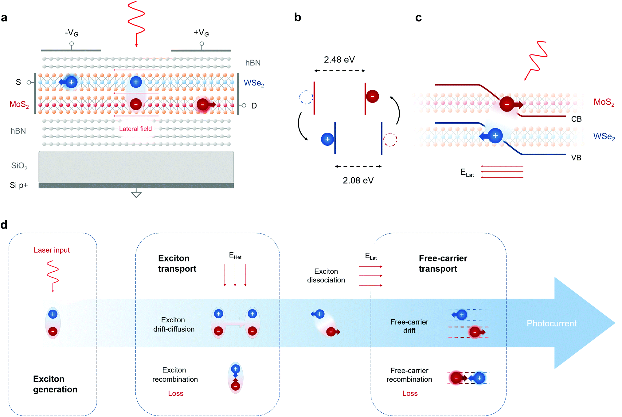 | ||
| Fig. 1 Device model and photocurrent extraction. (a) Schematic structure of the top split-gate photodetector. Interlayer excitons are generated by a light source focused on a WSe2/MoS2 heterobilayer. The top and bottom hBN layers form 10 nm and 30 nm thick dielectrics respectively. The substrate is made of SiO2 (270 nm) over heavily p-doped bulk silicon. Opposite gate voltages are applied to the left and right electrodes, thus inducing an electrostatically doped p–n junction along both TMDCs. Interlayer excitons are dissociated by a sufficiently high lateral electric field, free charges are drifted out of the junction and then diffuse to the lateral contacts. (b) Heterojunction bands with type-II alignment.39 Photogenerated electrons and holes tunnel within tens of femtoseconds31 to form interlayer excitons. (c) Schematic representation of interlayer exciton dissociation in the heterobilayer junction. The conduction band of MoS2 and the valence band of WSe2 are depicted in the condition of high and opposite electrostatic doping in both layers. (d) The process of photocurrent extraction can be divided in three main parts: exciton generation, exciton transport and free-carrier transport. Exciton transport is regulated by the excitonic potential, depending on the vertical electric field inside the heterostructure. The lateral field induces exciton dissociation and generates free carriers. The photocurrent depends on the free-carrier drift time induced by the lateral field inside the junction, as well as the recombination factors of free electrons and holes in the two TMDC layers. | ||
Results and discussion
Even though outstanding experimental research efforts are currently undertaken on the manipulation of exciton complexes in 2D materials, a detailed physical description of the mechanisms at play in devices based on interlayer exciton transport in van der Waals heterostructures is still lacking. In order to evaluate the performance of the split-gate photodetectors proposed in this work, we have developed a theoretical framework that includes the main physical phenomena of interest for interlayer exciton transport. Previous numerical calculations of the exciton potential energy have mainly considered analytical estimations of the Stark shift effect, neither accounting for exciton–exciton interaction nor employing the exact calculation of the electric field inside the heterostructure in the presence of electrostatic doping.26,40 Moreover, the drift-diffusion equation for interlayer excitons in van der Waals heterobilayers has been solved mainly through analytical formulas, neglecting the self-consistency with a varying exciton potential energy.28,41,42 Therefore, a fully comprehensive framework for interlayer exciton transport in van der Waals heterostructures is needed in order to fully address the involved physics and provide a theoretical basis for modeling excitonic transistors and circuits.43 In particular, we use a transfer-matrix method to study the propagation of the laser beam through the layered medium and extract the interlayer exciton generation factor in the WSe2/MoS2 heterobilayer (ESI† Note 1). The electrostatic potential in the simulated devices is computed solving the Poisson equation on NanoTCAD ViDES44 in a self-consistent loop with the calculation of the charge distributions in the 2D materials of the structure (ESI† Note 2). Interlayer exciton transport is then computed through the complete drift-diffusion equation including second-order factors in both the interlayer exciton potential energy and the exciton recombination term (ESI† Note 3).In order to validate the predictive capabilities of the implemented simulation platform, we solve the interlayer exciton diffusion considering the materials and optical characteristics of the first room-temperature excitonic transistor reported in the literature (Inset of Fig. 2c and Fig. S2a, ESI†).26 Since the normalized interlayer exciton density and photoluminescence (PL) can be assumed to be directly related, the 1D and 2D normalized solutions for steady-state exciton density distributions are compared with experimental PL data for a Gaussian laser beam (Fig. 2a). The extracted transport parameters for interlayer excitons in such a structure are aligned with other reports on interlayer exciton dynamics in WSe2/MoS2 van der Waals heterostructures, as well as in other type-II heterojunctions of TMDCs,28,31,40–42,45 while still being lower with respect to the best results ever obtained.28,41 We note that, by extracting the physical parameters from experimental results, we are inherently considering all the non-idealities in the interlayer exciton transport of a fabricated heterostructure, comprising the presence of defects. Nonetheless, future research could provide an accurate description of the effect of defect-bound states and defect-induced transitions on the variability of interlayer exciton transport parameters, which would be beneficial for the modeling of excitonic devices. In this work, second-order terms have been included in the simulation platform in order to consider factors such as exciton–exciton annihilation and Auger processes. Further information on the extraction and evaluation of the transport parameters is presented in detail in ESI† Note 3. For an optical power of 270 μW at a wavelength of 647 nm, the steady-state exciton density reaches a maximum value of 3.8 × 1011 cm−2 at the laser beam center point (x = 0). For high generation factors, similar distributions are obtained from the one- and two-dimensional solutions. We note that our results lie within the theoretical predictions for the exciton density limit in a WSe2/MoS2 heterobilayer.41,46
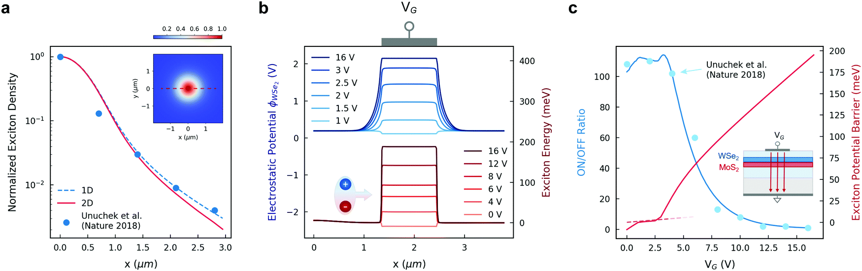 | ||
| Fig. 2 Interlayer exciton transport. (a) Exciton free diffusion for the full 2D transport (solid red line) and the 1D approximation (dashed blue line) along the heterobilayer. The blue points are extracted from the output photoluminescence induced by diffused interlayer excitons in the room-temperature excitonic transistor (Fig. S2a, ESI†).15 The 2D colormap plot of in-plane diffusion is reported in the inset. (b) Electrostatic potential ϕ on the WSe2 layer (blue) and exciton potential energy (red) for varying gate voltages. The gate region is highlighted by a schematic drawing on top of the graph. The behavior of the maximum ϕWse2 as function of the top-gate voltage is shown in Fig. S2c (ESI†), reporting a steep increase below VG = 2.5 V followed by a gradual saturation to a value close to the bandgap of the material. The exciton–exciton interaction (EEI) reaches its maximum at the highest exciton density (x = 0). A potential energy barrier is raised through the quantum-confined Stark effect for growing top-gate voltages, effectively impeding exciton diffusion. (c) The simulated ON/OFF ratio (blue line) of the excitonic transistor is compared to the corresponding data from the reference device (blue dots).26 The excitonic potential barrier height (solid red line) is confronted with a simple analytical formula (ESI† Note 2) in the VG region corresponding to lightly doped TMDC layers (dashed red line). A schematic representation of the excitonic transistor is represented in the inset. | ||
Next, we solve the electrostatics and drift-diffusion problems in the excitonic transistor. The simulated electrostatic potential on the WSe2 layer is reported in Fig. 2b, together with the extracted interlayer exciton potential energy U. A potential barrier is imposed with increasing gate voltages due to the Stark shift component in U, reaching values slightly under 200 meV for gate voltage VG = 16 V. The exciton–exciton interaction term (EEI, ESI† Note 3) follows the same spatial distribution as N, with a maximum value of 5.7 meV at x = 0, thus being only relevant for transport at low gate voltage. VG controls the potential barrier height and thus the exciton transport, determining the effective modulation of the interlayer exciton density beyond the gate region. The simulated ON/OFF ratio for the output interlayer exciton density is reported in Fig. 2c, showing very good agreement with the experimental data from the work of Unucheck et al.26 These results clearly demonstrate that the implemented approach is able to correctly foresee the behavior of an excitonic device. We further apply our method to engineer the excitonic transistor by geometrical optimization. In ESI† Note 4, we demonstrate that ON/OFF ratios can be improved if larger distances between the light beam focus and the output region are considered, with maximum ON/OFF ratios reaching values up to approximately 270 at the cost of reduced output exciton densities. We also determine that the excitonic transistor is a scalable device, with good performance at gate lengths as small as 100 nm, thus motivating further research on compact low-power optical interconnects based on interlayer excitons in van der Waals heterostructures.47
In order to assess the performance of the proposed photodetectors (Fig. 1a and Fig. S3, ESI†), we integrate the exact electrostatic solution in the van der Waals heterostructure for varying split-gate voltages with interlayer exciton drift-diffusion simulations and free-carrier transport equations (Fig. 1d, ESI† Note 5). The van der Waals heterostructure dimensions, the substrate and the laser wavelength are equivalent to those of the excitonic transistor, and thus the same transport parameters are valid (ESI† Note 3). The optical beam width is taken as equal to the diffraction-limited spot size of a 647 nm laser (∼820 nm). In all simulations, the voltage difference between the lateral contacts VDS is imposed to be null in order to consider near-equilibrium transport and demonstrate a fully photovoltaic detecting operation.
The split-gate voltage is varied between 0 V and 4 V, which is enough to cover the whole range of quantum efficiencies and responsivities that are achieved in our devices. The spatial maps of the lateral electric field in the heterostructure with VG = 4 V are reported in Fig. 3a and d for the top and bottom split-gate devices respectively. The electrostatic potential on the WSe2 monolayer and the lateral electric field in the heterobilayer vary with increasing top (Fig. 3b) and bottom (Fig. 3e) split-gate voltages. Sufficiently high voltages induce enough electrostatic doping to generate a lateral p–n junction with maximum voltage difference determined by the bandgap of the material. The different lateral electric field distributions in the two devices depend on the position of the split-gate electrodes with respect to both the back gate and the heterobilayer itself. With high voltages in the bottom split-gate structure, the effective junction length Leff is reduced compared to the nominal value (ESI† Note 6).
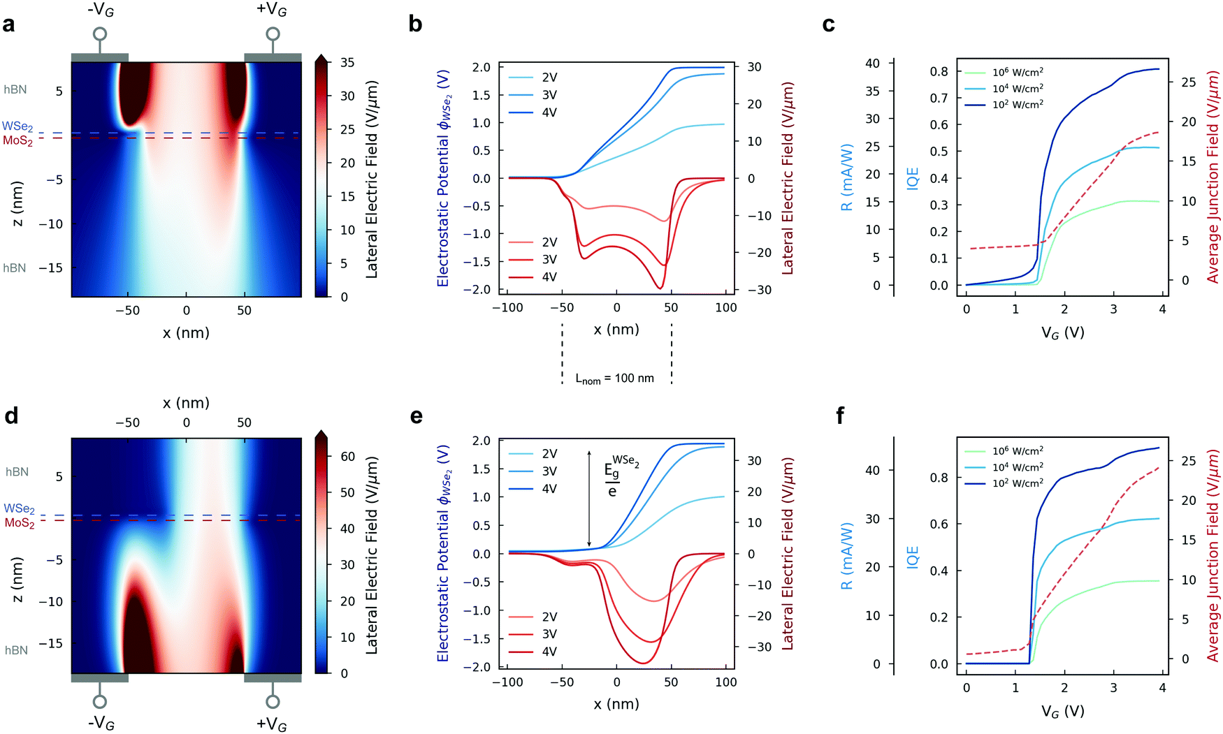 | ||
| Fig. 3 Electric field and photoresponse. (a and d) Electric field distributions in the heterostructure for VG = 4 V for top and bottom split-gate detectors, respectively. The color scale ranges are chosen for display purposes. (b and e) Electrostatic potential on WSe2 (blue) and lateral electric field (red) for different split-gate voltages in the top-gate and bottom-gate photodetectors respectively. The nominal length of the junction region is highlighted on the results in the top-gate geometry. (c and f) Average lateral electric field (red), responsivity and internal quantum efficiency (blue) as a function of the split-gate voltage in the two devices of interest for different power densities. | ||
The simulated responsivities and IQEs of the devices are reported in Fig. 3c and f as a function of VG, together with the average lateral electric fields inside the effective junction regions. A steep increase in responsivity is observed at electric fields higher than 4 V μm−1. Thus, we can define the threshold voltage for photodetection as the VG corresponding to ELat ≃4 V μm−1. Photodetection threshold voltages in the range between 1.2 V and 1.5 V are obtained for both device geometries, with shifts for different optical power densities due to the nonlinear recombination term. All responsivity curves saturate at higher electric fields, where the main limiting transport mechanism is free-carrier drift.
The split-gate separation in our device model is a fraction of the laser beam spot diameter (d ∼8 Lnom). Thus, a significant portion of the total interlayer exciton population is generated outside of the junction region. These excitons can diffuse along the van der Waals heterobilayer and reach the region between the split gates. The collection efficiency in split-gate detectors with excitonic species is defined as the ratio between the number of excitons that reach the p–n junction region and the total generated population. In the low-density regime, high collection efficiencies can be obtained thanks to the micrometer-scale diffusion length of interlayer excitons in our system (ESI† Note 3). At low optical power densities (I0 ≤ 105 W m−2), the responsivities in the top and bottom split-gate devices reach values of 41 mA W−1 and 47 mA W−1, corresponding to internal quantum efficiencies as high as 83% and 95%, respectively. However, for high optical power densities (I0 > 105 W m−2), the second order term in the recombination factor dominates the quasiparticle dynamics, and the excitons generated outside of the junction are forced to recombine before they can reach the high-field region (ESI† Note 7). Thus, high optical power densities lead to lower maximum responsivities (Fig. 3e and f). A complete power-dependent study of the device performance is reported in Fig. S7 (ESI†) for both top and bottom split-gate photodetectors. Similarly, bigger spot sizes also contribute in diminishing the responsivity in the devices due to the higher distance between the generated electron–hole pairs and the high-field region (Fig. S8, ESI†). We have also investigated the variability of the maximum responsivities and photoresponse rates in the two device geometries with respect to split-gate separation and free-carrier mobility (Fig. S9 and S10, ESI†).
In the low-density regime, the intrinsic photoresponse rate in the devices can be estimated as Γph ≃ 1/(τN + τn),13 where τN and τn are the exciton decay time and the free-carrier lifetime respectively. We extract the rates for both detector geometries at different split-gate voltages (Fig. 4). We note that our simulations consider intrinsic photoresponse rates following experimental works on time-resolved photocurrent measurements of ultrafast detectors based on p–n junctions.12,13,48,49 In this picture, the limiting mechanisms to the device performance lie in the carrier dynamics inside the junction region, as for the intrinsic photoresponse of traditional photodiodes. Extrinsic terms, such as resistive-capacitive parasitic components, are strictly dependent on device fabrication and measurement equipment, and can be properly engineered based on the available technology.8 For low junction fields (0 V ≤ VG ≤ 1.2 V) the response rate of the bottom split-gate device is dominated by exciton recombination. In the top split-gate geometry, the lateral field does not go to zero for low VG, and therefore the photoresponse rate depends on both recombination and dissociation for low fields. For moderate fields (1.2 V < VG < 1.6 V), interlayer exciton dissociation is the main physical phenomena that limits photocurrent extraction in both devices, while for VG ≥1.6 V the junction fields are high enough that free-carrier drift becomes the dominating mechanism in the photoresponse. For VG = 4 V, i.e. in the highest responsivity range, we obtain response times of 3.8 ps and 5.7 ps in the bottom and top split-gate detectors respectively, demonstrating high-sensitivity and high-speed photodetectors based on type-II TMDC heterobilayers. In Table 1, the performance of the proposed devices is compared to that of the fastest state-of-the-art detectors based on 2D materials reported in the literature.
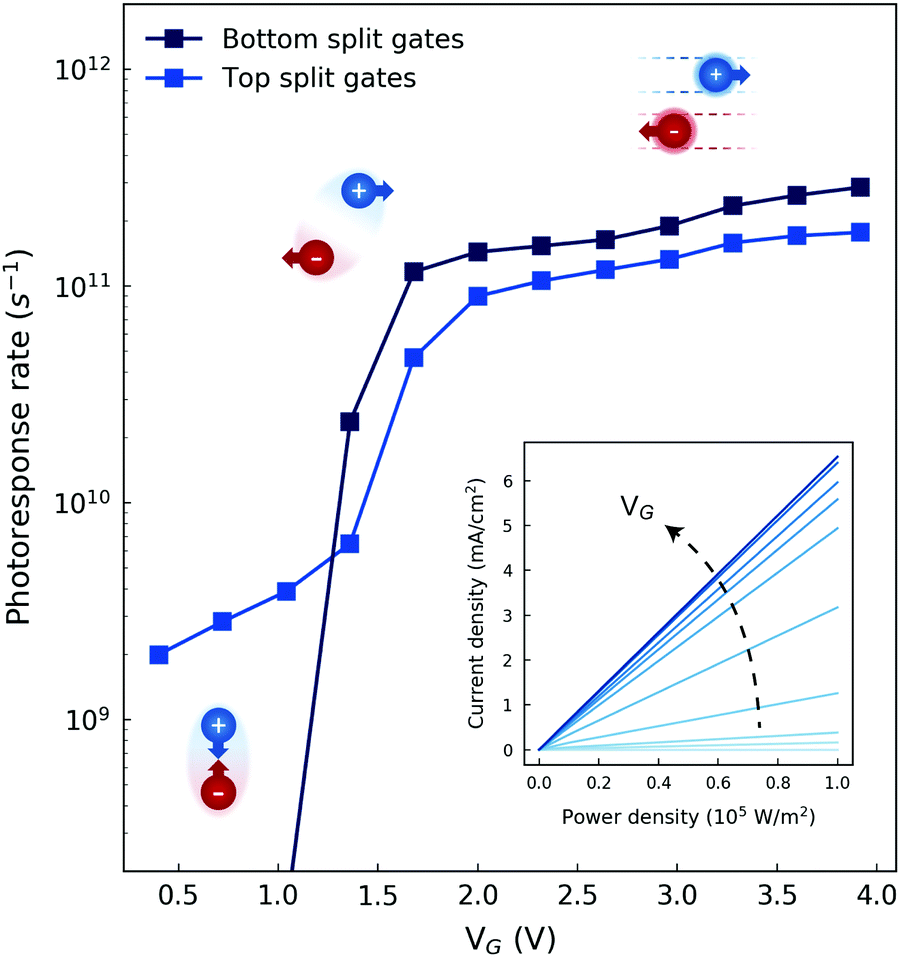 | ||
| Fig. 4 Photoresponse rate and linearity. Intrinsic photoresponse rate in the bottom and top split-gate detectors as a function of VG. The voltage ranges corresponding to low, moderate and high fields show responses dominated by exciton recombination, dissociation and free-carrier drift respectively. Inset: Output photocurrent density as a function of input optical power density for varying average junction fields. A highly linear behavior is reported for the considered range of input light intensity. | ||
| Structure | Wavelength (nm) | Photoresponse Time (ps) | Bandwidth (GHz) | IQE (%) | Responsivity (mA W−1) |
|---|---|---|---|---|---|
| ∼, value extracted from plots or estimated from other parameters. *, intrinsic value not considering extrinsic terms. Comparison between ultrafast photodetectors in the state of the art and the encapsulated WSe2/MoS2 heterostructure device proposed in our work. We are considering detectors with photovoltaic operation (zero bias), response times under 1 ns and responsivities higher than 1 mA W−1. | |||||
| Graphene8 | 1550 | — | 40 | 6–16 | 0.5 |
| Graphene51 | 1550 | 2.1* | 262* | 16–37 | — |
| Graphene/WSe2/Graphene12 | 800 | 5.5* | 100* | 40 | ∼1.5 |
| Monolayer WSe213 | 750 | ∼20* | ∼27.5* | 15 | ≤4.5 |
| Waveguide-integrated graphene11 | 1550 | 24 | 18 | 87 | ∼48 |
| Waveguide-integrated graphene/MoTe217 | 1300 | ∼18 | ∼30 | <40 | ≤10 |
| WSe2/MoS2 heterobilayer (this work) | 647 | 3.5–5.7* | ∼96–145* | 80–95 | 41–49 |
We note that the charge-transfer efficiency in type-II TMDC heterojunctions is dependent on the lateral electric field.29 Since the optically excited electrons and holes form spatially indirect excitons on ultrafast time scales (∼50 fs) with near-unity charge transfer efficiencies,31–35 we assume that interlayer excitons in the WSe2/MoS2 heterobilayer form significantly faster with respect to intralayer exciton dissociation for low lateral electric fields. Indeed, for ELat ≤15 V μm−1, where most of the photoresponse modulation in our devices takes place, intralayer exciton dissociation occurs in the order of tens of picoseconds. For higher fields, the two physical mechanisms concur and a portion of the generated intralayer excitons dissociate before tunneling. However, for ELat >15 V μm−1, both the responsivity (Fig. 3c and f) and speed (Fig. 4) of the proposed devices are limited by free-carrier transport (Fig. S4, ESI†). Thus, for high lateral fields, the intralayer excitons that dissociate before undergoing charge transfer will equivalently contribute to the extracted photocurrent as the successfully formed and dissociated interlayer excitons. Therefore, the interplay between intralayer dissociation and charge transfer is not relevant in our study for both low and high lateral fields, and the extracted photocurrent is indeed modulated by interlayer exciton dissociation.
Finally, we have investigated the heterobilayer photodetectors linearity. This aspect is especially relevant in artificial neural networks based on photodetector arrays, where the input optical power density and the output photocurrent density vectors are related through a responsivity matrix where the network weights are encoded.10 Thus, linearity between input and output quantities is required in the matrix-vector product operation Jout = R Iin. The output photocurrent density in our devices is reported in the inset of Fig. 4 as a function of input light intensity for different junction electric fields, showing a highly linear behavior for Iin < 105 W m−2. Further investigations on power dependence are reported in ESI† Note 7. The considered ELat range corresponds to the moderate field region, where most of the photocurrent span is contained for both devices (Fig. 3c and f). We note that linearity can also be achieved for higher optical powers by appropriately restricting the operative range based on the actual photocurrent behavior.
Conclusions
We have proposed novel photodetectors through the development of a purposely devised simulation platform for interlayer exciton transport in van der Waals heterostructures of 2D materials. We have validated the model against experimental results of excitonic devices available in the literature, showing excellent agreement. Leveraging the demonstrated predictive capabilities of the proposed simulation framework, we have assessed the performance of the proposed heterobilayer photodetectors, showing high internal quantum efficiencies up to 95% and maximum responsivities around 47 mA W−1 with response times below 4 ps. The responsivities and IQEs of the detectors depend on the lateral electric field of an electrostatically induced p–n junction, which can be varied by changing the voltage applied to the split-gate electrodes. It is worth noting that the proposed photodetectors can be readily realized with the current available fabrication technology of van der Waals heterostructures and no additional challenges arise from our design. Even though the performance of the proposed detectors is limited to the visible spectrum, the developed device model and operating principle can be equivalently applied to van der Waals heterostructures with interlayer transitions in the infrared range.36–38,50 Furthermore, detectors with tunable responsivities operated in photovoltaic mode allow for the realization of monolithically integrated image sensors with zero latency and self-powered operation.10 With the proposed devices, it is possible to realize artificial neural networks (ANNs) for machine vision in a 30 mA W−1 responsivity range with gate voltage variations as low as 300 mV. A full total range up to 94 mA W−1 is also available at the cost of split-gate voltage sweeps in the range between −2 V and +2 V.In conclusion, we predict that photodetectors based on interlayer excitons in WSe2/MoSe2 heterobilayers can yield an unprecedented trade-off between speed and responsivity, opening new perspectives on ultrafast photodetectors based on 2D materials, and triggering an interest towards the experimental fabrication of the proposed devices. Moreover, their array integration as pixels could enable future artificial neural networks for picosecond time-resolved spectroscopy and other ultrafast applications in machine vision.
Methods
Optical input
A transfer-matrix method52,53 is applied to study the propagation of the laser beam electromagnetic waves through the layered media in the devices of interest. The optical power dissipated in each layer is extracted by adapting known procedures in common bulk photovoltaics to structures based on 2D materials.54 Then, interlayer exciton generation rates in the TMDC layers of the structure are calculated by including charge transfer in type-II heterobilayers (ESI† Note 1).Electrostatics
The Poisson equation is solved through the NanoTCAD ViDES simulation software44,55 with a classical box-method discretization in rectangular domains. In order to obtain the exact electrostatic solution in the structure, we have considered the semiconducting behavior of the TMDCs. A self-consistent loop between the Poisson equation and the charge distribution in the TMDCs is iterated through the Newton-Raphson method (ESI† Note 2). Electron and hole densities in the semiconducting layers are calculated following an effective-mass approximation in the expression for 2D-confined charge distributions and Fermi-Diract statistics.Interlayer exciton transport
The steady-state drift-diffusion equation for interlayer exciton transport in the classical limit56 is solved in a rectangular grid box-method with Scharfetter-Gummel discretization in both one and two dimensions. The excitonic potential and the recombination factor are calculated considering second order terms in a complete theoretical framework (ESI† Note 3). A decoupled Gummel map method is specifically developed by including the device electrostatics and interlayer exciton transport in a single simulation flow. For a given electrostatic solution, which sets the initial excitonic potential and recombination term, the potential and population densities of interlayer excitons are derived through an iterative scheme until convergence. For the photodetectors proposed in this work, dissociation rates and free-carrier dynamics are included in the framework in order to calculate photocurrent extraction and the detector parameters of interest.Author contributions
E. L. developed the simulation platform and modeled the devices. E. G. M. developed the self-consistent solution to the electrostatic problem. G. F. initiated and supervised the research. All authors discussed the results and contributed to the manuscript.Conflicts of interest
The authors declare no competing interests.Acknowledgements
E. G. M. acknowledges Juan de la Cierva Incorporación IJCI-2017-32297 (MINECO/AEI). G.F gratefully acknowledges Graphene Flagship Core 3 (Contract No. 881603).References
- Q. H. Wang, K. Kalantar-Zadeh, A. Kis, J. N. Coleman and M. S. Strano, Electronics and Optoelectronics of Two-Dimensional Transition Metal Dichalcogenides, Nat. Nanotechnol., 2012, 7(11), 699–712, DOI:10.1038/nnano.2012.193.
- F. H. L. Koppens, T. Mueller, P. Avouris, A. C. Ferrari, M. S. Vitiello and M. Polini, Photodetectors Based on Graphene, Other Two-Dimensional Materials and Hybrid Systems, Nat. Nanotechnol., 2014, 9(10), 780–793, DOI:10.1038/nnano.2014.215.
- K. Kim, J.-Y. Choi, T. Kim, S.-H. Cho and H.-J. Chung, A Role for Graphene in Silicon-Based Semiconductor Devices, Nature, 2011, 479(7373), 338–344, DOI:10.1038/nature10680.
- L. Britnell, R. M. Ribeiro, A. Eckmann, R. Jalil, B. D. Belle, A. Mishchenko, Y.-J. Kim, R. V. Gorbachev, T. Georgiou, S. V. Morozov, A. N. Grigorenko, A. K. Geim, C. Casiraghi, A. H. C. Neto and K. S. Novoselov, Strong Light-Matter Interactions in Heterostructures of Atomically Thin Films, Science, 2013, 340(6138), 1311–1314, DOI:10.1126/science.1235547.
- T. Mueller and E. Malic, Exciton Physics and Device Application of Two-Dimensional Transition Metal Dichalcogenide Semiconductors, npj 2D Mater. Appl., 2018, 2(1), 1–12, DOI:10.1038/s41699-018-0074-2.
- G. Konstantatos, Current Status and Technological Prospect of Photodetectors Based on Two-Dimensional Materials, Nat. Commun., 2018, 9(1), 5266, DOI:10.1038/s41467-018-07643-7.
- P. Ma, Y. Salamin, B. Baeuerle, A. Josten, W. Heni, A. Emboras and J. Leuthold, Plasmonically Enhanced Graphene Photodetector Featuring 100 Gbit/s Data Reception, High Responsivity, and Compact Size, ACS Photonics, 2019, 6(1), 154–161, DOI:10.1021/acsphotonics.8b01234.
- F. Xia, T. Mueller, Y. Lin, A. Valdes-Garcia and P. Avouris, Ultrafast Graphene Photodetector, Nat. Nanotechnol., 2009, 4(12), 839–843, DOI:10.1038/nnano.2009.292.
- T. Mueller, F. Xia and P. Avouris, Graphene Photodetectors for High-Speed Optical Communications, Nat. Photonics, 2010, 4(5), 297–301, DOI:10.1038/nphoton.2010.40.
- L. Mennel, J. Symonowicz, S. Wachter, D. K. Polyushkin, A. J. Molina-Mendoza and T. Mueller, Ultrafast Machine Vision with 2D Material Neural Network Image Sensors, Nature, 2020, 579(7797), 62–66, DOI:10.1038/s41586-020-2038-x.
- S. Schuler, D. Schall, D. Neumaier, B. Schwarz, K. Watanabe, T. Taniguchi and T. Mueller, Graphene Photodetector Integrated on a Photonic Crystal Defect Waveguide, ACS Photonics, 2018, 5(12), 4758–4763, DOI:10.1021/acsphotonics.8b01128.
- M. Massicotte, P. Schmidt, F. Vialla, K. G. Schädler, A. Reserbat-Plantey, K. Watanabe, T. Taniguchi, K. J. Tielrooij and F. H. L. Koppens, Picosecond Photoresponse in van der Waals Heterostructures, Nat. Nanotechnol., 2016, 11(1), 42–46, DOI:10.1038/nnano.2015.227.
- M. Massicotte, F. Vialla, P. Schmidt, M. B. Lundeberg, S. Latini, S. Haastrup, M. Danovich, D. Davydovskaya, K. Watanabe, T. Taniguchi, V. I. Fal’ko, K. S. Thygesen, T. G. Pedersen and F. H. L. Koppens, Dissociation of Two-Dimensional Excitons in Monolayer WSe2, Nat. Commun., 2018, 9(1), 1633, DOI:10.1038/s41467-018-03864-y.
- A. K. Geim and I. V. Grigorieva, van der Waals Heterostructures, Nature, 2013, 499(7459), 419–425, DOI:10.1038/nature12385.
- S. Kar, Y. Su, R. R. Nair and A. K. Sood, Probing Photoexcited Carriers in a Few-Layer MoS2 Laminate by Time-Resolved Optical Pump–Terahertz Probe Spectroscopy, ACS Nano, 2015, 9(12), 12004–12010, DOI:10.1021/acsnano.5b04804.
- W. Zheng, M. Bonn and H. I. Wang, Photoconductivity Multiplication in Semiconducting Few-Layer MoTe2, Nano Lett., 2020, 20(8), 5807–5813, DOI:10.1021/acs.nanolett.0c01693.
- N. Flöry, P. Ma, Y. Salamin, A. Emboras, T. Taniguchi, K. Watanabe, J. Leuthold and L. Novotny, Waveguide-Integrated van der Waals Heterostructure Photodetector at Telecom Wavelengths with High Speed and High Responsivity, Nat. Nanotechnol., 2020, 15(2), 118–124, DOI:10.1038/s41565-019-0602-z.
- J. Liao, B. Sa, J. Zhou, R. Ahuja and Z. Sun, Design of High-Efficiency Visible-Light Photocatalysts for Water Splitting: MoS2/AlN(GaN) Heterostructures, J. Phys. Chem. C, 2014, 118(31), 17594–17599, DOI:10.1021/jp5038014.
- Z. Guo, N. Miao, J. Zhou, B. Sa and Z. Sun, Strain-Mediated Type-I/Type-II Transition in MXene/Blue Phosphorene van der Waals Heterostructures for Flexible Optical/Electronic Devices, J. Mater. Chem. C, 2017, 5(4), 978–984, 10.1039/C6TC04349F.
- J. Chen, X. He, B. Sa, J. Zhou, C. Xu, C. Wen and Z. Sun, III–VI van der Waals Heterostructures for Sustainable Energy Related Applications, Nanoscale, 2019, 11(13), 6431–6444, 10.1039/C9NR00421A.
- D. K. Singh, R. Pant, A. M. Chowdhury, B. Roul, K. K. Nanda and S. B. Krupanidhi, Defect-Mediated Transport in Self-Powered, Broadband, and Ultrafast Photoresponse of a MoS 2/AlN/Si-Based Photodetector, ACS Appl. Electron. Mater., 2020, 2(4), 944–953, DOI:10.1021/acsaelm.0c00007.
- P. Rivera, J. R. Schaibley, A. M. Jones, J. S. Ross, S. Wu, G. Aivazian, P. Klement, K. Seyler, G. Clark, N. J. Ghimire, J. Yan, D. G. Mandrus, W. Yao and X. Xu, Observation of Long-Lived Interlayer Excitons in Monolayer MoSe2 –WSe2 Heterostructures, Nat. Commun., 2015, 6(1), 6242, DOI:10.1038/ncomms7242.
- M. Palummo, M. Bernardi and J. C. Grossman, Exciton Radiative Lifetimes in Two-Dimensional Transition Metal Dichalcogenides, Nano Lett., 2015, 15(5), 2794–2800, DOI:10.1021/nl503799t.
- Y. Yu, S. Hu, L. Su, L. Huang, Y. Liu, Z. Jin, A. A. Purezky, D. B. Geohegan, K. W. Kim, Y. Zhang and L. Cao, Equally Efficient Interlayer Exciton Relaxation and Improved Absorption in Epitaxial and Nonepitaxial MoS2/WS2 Heterostructures, Nano Lett., 2015, 15(1), 486–491, DOI:10.1021/nl5038177.
- G. Grosso, J. Graves, A. T. Hammack, A. A. High, L. V. Butov, M. Hanson and A. C. Gossard, Excitonic Switches Operating at around 100 K, Nat. Photonics, 2009, 3(10), 577–580, DOI:10.1038/nphoton.2009.166.
- D. Unuchek, A. Ciarrocchi, A. Avsar, K. Watanabe, T. Taniguchi and A. Kis, Room-Temperature Electrical Control of Exciton Flux in a van der Waals Heterostructure, Nature, 2018, 560(7718), 340–344, DOI:10.1038/s41586-018-0357-y.
- A. Ciarrocchi, D. Unuchek, A. Avsar, K. Watanabe, T. Taniguchi and A. Kis, Polarization Switching and Electrical Control of Interlayer Excitons in Two-Dimensional van der Waals Heterostructures, Nat. Photonics, 2019, 13(2), 131–136, DOI:10.1038/s41566-018-0325-y.
- D. Unuchek, A. Ciarrocchi, A. Avsar, Z. Sun, K. Watanabe, T. Taniguchi and A. Kis, Valley-Polarized Exciton Currents in a van der Waals Heterostructure, Nat. Nanotechnol., 2019, 14(12), 1104–1109, DOI:10.1038/s41565-019-0559-y.
- H. C. Kamban and T. G. Pedersen, Interlayer Excitons in van der Waals Heterostructures: Binding Energy, Stark Shift, and Field-Induced Dissociation, Sci. Rep., 2020, 10(1), 5537, DOI:10.1038/s41598-020-62431-y.
- B. Peng, G. Yu, X. Liu, B. Liu, X. Liang, L. Bi, L. Deng, T. C. Sum and K. P. Loh, Ultrafast Charge Transfer in MoS2/WSe2 p–n Heterojunction, 2D Mater., 2016, 3(2), 025020, DOI:10.1088/2053-1583/3/2/025020.
- J. Kim, C. Jin, B. Chen, H. Cai, T. Zhao, P. Lee, S. Kahn, K. Watanabe, T. Taniguchi, S. Tongay, M. F. Crommie and F. Wang, Observation of Ultralong Valley Lifetime in WSe2/MoS2 Heterostructures, Sci. Adv., 2017, 3(7), e1700518, DOI:10.1126/sciadv.1700518.
- X. Hong, J. Kim, S.-F. Shi, Y. Zhang, C. Jin, Y. Sun, S. Tongay, J. Wu, Y. Zhang and F. Wang, Ultrafast Charge Transfer in Atomically Thin MoS2/WS2 Heterostructures, Nat. Nanotechnol., 2014, 9(9), 682–686, DOI:10.1038/nnano.2014.167.
- F. Ceballos, M. Z. Bellus, H.-Y. Chiu and H. Zhao, Ultrafast Charge Separation and Indirect Exciton Formation in a MoS2–MoSe2 van der Waals Heterostructure, ACS Nano, 2014, 8(12), 12717–12724, DOI:10.1021/nn505736z.
- H. Chen, X. Wen, J. Zhang, T. Wu, Y. Gong, X. Zhang, J. Yuan, C. Yi, J. Lou, P. M. Ajayan, W. Zhuang, G. Zhang and J. Zheng, Ultrafast Formation of Interlayer Hot Excitons in Atomically Thin MoS2/WS2 Heterostructures, Nat. Commun., 2016, 7(1), 12512, DOI:10.1038/ncomms12512.
- Y. Li, H. Zhou, Y. Chen, Y. Zhao and H. Zhu, Efficient Hot-Electron Extraction in Two-Dimensional Semiconductor Heterostructures by Ultrafast Resonant Transfer, J. Chem. Phys., 2020, 153(4), 044705, DOI:10.1063/5.0018072.
- K. Zhang, T. Zhang, G. Cheng, T. Li, S. Wang, W. Wei, X. Zhou, W. Yu, Y. Sun, P. Wang, D. Zhang, C. Zeng, X. Wang, W. Hu, H. J. Fan, G. Shen, X. Chen, X. Duan, K. Chang and N. Dai, Interlayer Transition and Infrared Photodetection in Atomically Thin Type-II MoTe2/MoS2 van der Waals Heterostructures, ACS Nano, 2016, 10(3), 3852–3858, DOI:10.1021/acsnano.6b00980.
- S. Lukman, L. Ding, L. Xu, Y. Tao, A. C. Riis-Jensen, G. Zhang, Q. Y. S. Wu, M. Yang, S. Luo, C. Hsu, L. Yao, G. Liang, H. Lin, Y.-W. Zhang, K. S. Thygesen, Q. J. Wang, Y. Feng and J. Teng, High Oscillator Strength Interlayer Excitons in Two-Dimensional Heterostructures for Mid-Infrared Photodetection, Nat. Nanotechnol., 2020, 15(8), 675–682, DOI:10.1038/s41565-020-0717-2.
- T. Qi, Y. Gong, A. Li, X. Ma, P. Wang, R. Huang, C. Liu, R. Sakidja, J. Z. Wu, R. Chen and L. Zhang, Interlayer Transition in a VdW Heterostructure toward Ultrahigh Detectivity Shortwave Infrared Photodetectors, Adv. Funct. Mater., 2020, 30(3), 1905687, DOI:10.1002/adfm.201905687.
- S. Latini, K. T. Winther, T. Olsen and K. S. Thygesen, Interlayer Excitons and Band Alignment in MoS2/HBN/WSe2 van der Waals Heterostructures, Nano Lett., 2017, 17(2), 938–945, DOI:10.1021/acs.nanolett.6b04275.
- Z. Wang, Y.-H. Chiu, K. Honz, K. F. Mak and J. Shan, Electrical Tuning of Interlayer Exciton Gases in WSe2 Bilayers, Nano Lett., 2018, 18(1), 137–143, DOI:10.1021/acs.nanolett.7b03667.
- L. A. Jauregui, A. Y. Joe, K. Pistunova, D. S. Wild, A. A. High, Y. Zhou, G. Scuri, K. D. Greve, A. Sushko, C.-H. Yu, T. Taniguchi, K. Watanabe, D. J. Needleman, M. D. Lukin, H. Park and P. Kim, Electrical Control of Interlayer Exciton Dynamics in Atomically Thin Heterostructures, Science, 2019, 366(6467), 870–875, DOI:10.1126/science.aaw4194.
- J. Choi, W.-T. Hsu, L.-S. Lu, L. Sun, H.-Y. Cheng, M.-H. Lee, J. Quan, K. Tran, C.-Y. Wang, M. Staab, K. Jones, T. Taniguchi, K. Watanabe, M.-W. Chu, S. Gwo, S. Kim, C.-K. Shih, X. Li and W.-H. Chang, Moiré Potential Impedes Interlayer Exciton Diffusion in van der Waals Heterostructures, Sci. Adv., 2020, 6(39), eaba8866, DOI:10.1126/sciadv.aba8866.
- Y. Liu, K. Dini, Q. Tan, T. Liew, K. S. Novoselov and W. Gao, Electrically Controllable Router of Interlayer Excitons, Sci. Adv., 2020, 6(41), eaba1830, DOI:10.1126/sciadv.aba1830.
- ViDES NanoTCAD .
- J. Binder, J. Howarth, F. Withers, M. R. Molas, T. Taniguchi, K. Watanabe, C. Faugeras, A. Wysmolek, M. Danovich, V. I. Fal’ko, A. K. Geim, K. S. Novoselov, M. Potemski and A. Kozikov, Upconverted Electroluminescence via Auger Scattering of Interlayer Excitons in van der Waals Heterostructures, Nat. Commun., 2019, 10(1), 2335, DOI:10.1038/s41467-019-10323-9.
- M. M. Fogler, L. V. Butov and K. S. Novoselov, High-Temperature Superfluidity with Indirect Excitons in van der Waals Heterostructures, Nat. Commun., 2014, 5(1), 4555, DOI:10.1038/ncomms5555.
- M. Baldo and V. Stojanović, Excitonic Interconnects, Nat. Photonics, 2009, 3(10), 558–560, DOI:10.1038/nphoton.2009.178.
- N. M. Gabor, Z. Zhong, K. Bosnick and P. L. McEuen, Ultrafast Photocurrent Measurement of the Escape Time of Electrons and Holes from Carbon Nanotube p–i–n Photodiodes, Phys. Rev. Lett., 2012, 108(8), 087404, DOI:10.1103/PhysRevLett.108.087404.
- J. Yin, Z. Tan, H. Hong, J. Wu, H. Yuan, Y. Liu, C. Chen, C. Tan, F. Yao, T. Li, Y. Chen, Z. Liu, K. Liu and H. Peng, Ultrafast and Highly Sensitive Infrared Photodetectors Based on Two-Dimensional Oxyselenide Crystals, Nat. Commun., 2018, 9(1), 3311, DOI:10.1038/s41467-018-05874-2.
- G. Wang, L. Li, W. Fan, R. Wang, S. Zhou, J.-T. Lü, L. Gan and T. Zhai, Interlayer Coupling Induced Infrared Response in WS2/MoS2 Heterostructures Enhanced by Surface Plasmon Resonance, Adv. Funct. Mater., 2018, 28(22), 1800339, DOI:10.1002/adfm.201800339.
- A. Urich, K. Unterrainer and T. Mueller, Intrinsic Response Time of Graphene Photodetectors, Nano Lett., 2011, 11(7), 2804–2808, DOI:10.1021/nl2011388.
- O. S. Heavens, Optical Properties of Thin Solid Films; Courier Corporation, 1991 Search PubMed.
- R. M. A. Azzam, N. M. Bashara and S. S. Ballard, Ellipsometry and Polarized Light, Phys. Today, 1978, 31, 72, DOI:10.1063/1.2994821.
- L. A. A. Pettersson, L. S. Roman and O. Inganäs, Modeling Photocurrent Action Spectra of Photovoltaic Devices Based on Organic Thin Films, J. Appl. Phys., 1999, 86(1), 487–496, DOI:10.1063/1.370757.
- G. Fiori and G. Iannaccone, Multiscale Modeling for Graphene-Based Nanoscale Transistors, Proc. IEEE, 2013, 101(7), 1653–1669, DOI:10.1109/JPROC.2013.2259451.
- A. L. Ivanov, Quantum Diffusion of Dipole-Oriented Indirect Excitons in Coupled Quantum Wells, EPL, 2002, 59(4), 586, DOI:10.1209/epl/i2002-00144-3.
Footnotes |
| † Electronic supplementary information (ESI) available. See DOI: 10.1039/d1nh00396h |
| ‡ Present address: Electrical Engineering Institute and Institute of Materials Science and Engineering, École Polytechnique Fédérale de Lausanne (EPFL), Lausanne, Switzerland. E-mail: edoardo.lopriore@epfl.ch, gianluca.fiori@unipi.it |
| This journal is © The Royal Society of Chemistry 2022 |