
 Open Access Article
 This Open Access Article is licensed under a Creative Commons Attribution-Non Commercial 3.0 Unported Licence
Improving the conductivity of graphite-based films by rapid laser annealing†
Gulsum
Ersu
a,
Sruthi
Kuriakose
a,
Stuart J.
Goldie
 b,
Abdullah M.
Al-Enizi
c,
Ayman
Nafady
c,
Carmen
Munuera
a,
Claudia
Backes
b,
Joshua O.
Island
*d and
Andres
Castellanos-Gomez
*a
b,
Abdullah M.
Al-Enizi
c,
Ayman
Nafady
c,
Carmen
Munuera
a,
Claudia
Backes
b,
Joshua O.
Island
*d and
Andres
Castellanos-Gomez
*a
aMaterials Science Factory, Instituto de Ciencia de Materiales de Madrid (ICMM-CSIC), Madrid, E-28049, Spain. E-mail: Andres.castellanos@csic.es
bPhysical Chemistry of Nanomaterials, University of Kassel, Germany
cDepartment of Chemistry, College of Science, King Saud University, Riyadh, 11451, Saudi Arabia
dDepartment of Physics and Astronomy, University of Nevada Las Vegas, Las Vegas, NV 89154, USA. E-mail: Joshua.island@unlv.edu
First published on 20th September 2022
Abstract
We present a method to anneal devices based on graphite films on paper and polycarbonate substrates. The devices are created using four different methods: spray-on films, graphite pencil-drawn films, liquid-phase exfoliated graphite films, and graphite powder abrasion-applied films. We characterize the optical properties of the films before and after laser annealing and report the two-terminal resistance of the devices for increased laser power density. We find the greatest improvement (16× reduction) in the resistance of spray-on film devices starting from 25.0 kΩ and reaching 1.6 kΩ at the highest annealing power densities. These improvements are attributed to local laser ablation of binders, stabilizers, and solvent residues left in the film after fabrication. This work highlights the utility of focused laser annealing for spray-on, drawn, printed, and abrasion fabricated films on substrates sensitive to heat/thermal treatments.
Since the isolation of graphene by mechanical exfoliation of graphite in 2004, a great deal of effort and resources have been invested in developing processes capable of synthesizing nanosheets of van der Waals materials in large quantities and at low cost.1–4 Different liquid phase exfoliation strategies have provided a very suitable way to achieve suspensions of few-layer flakes at low cost and using processes that can be easily scaled up to industrial requirements.5–8 These colloidal suspensions with flakes of van der Waals materials are particularly suited for use in many printing deposition methods in what is called, printed electronics.9–13 The conductivity of the films achieved by these techniques, however, tends to be highly varied (2 Ω sq−1 to
![[thin space (1/6-em)]](https://www.rsc.org/images/entities/char_2009.gif) 2 × 10⁵ Ω sq−1) and limited by poor flake to flake contact that is attributed to the presence of stabilizers, adsorbates, and solvent residues trapped within the flake network.14 Several reports have focused on finding routes to tackle this open challenge, with thermal treatments (annealing) being the most widespread methods.15,16 Nonetheless, conventional annealing processes might not be compatible with substrates like paper or certain polymers as they tend to degrade and even fail/break upon moderate temperature annealing over long periods of time. Laser-induced heating can be an alternative to traditional annealing processes, using hotplates or ovens. In fact, laser-based annealing has been used to clean graphene films of poly(methyl methacrylate) (PMMA) residues left after micro-fabrication,17 to reduce graphene oxide18 and even to anneal printed graphite films.19,20 To our knowledge, laser-annealing has not been implemented to anneal paper-supported films so far.
2 × 10⁵ Ω sq−1) and limited by poor flake to flake contact that is attributed to the presence of stabilizers, adsorbates, and solvent residues trapped within the flake network.14 Several reports have focused on finding routes to tackle this open challenge, with thermal treatments (annealing) being the most widespread methods.15,16 Nonetheless, conventional annealing processes might not be compatible with substrates like paper or certain polymers as they tend to degrade and even fail/break upon moderate temperature annealing over long periods of time. Laser-induced heating can be an alternative to traditional annealing processes, using hotplates or ovens. In fact, laser-based annealing has been used to clean graphene films of poly(methyl methacrylate) (PMMA) residues left after micro-fabrication,17 to reduce graphene oxide18 and even to anneal printed graphite films.19,20 To our knowledge, laser-annealing has not been implemented to anneal paper-supported films so far.
Herein, we tested an annealing process using a focalized laser beam. The laser is raster-scanned over the area to be annealed, allowing for spatially variable annealing. With a localized laser spot, a significant amount of heat can be generated on the film in a short amount of time without damaging the substrate underneath. We have probed this annealing method with films of interconnected graphite nanosheets deposited by brushing, printing, spraying, and abrasion techniques on a standard copy paper and polycarbonate substrates and found that laser annealing decreases electrical resistance by up to 16× for spray-on graphite on paper and 15× on polycarbonate substrates. The capability of generating spatially variable conductivity profiles is also demonstrated in the deposited films, opening the door to use laser induced annealing to add new functionality to deposited films.
We use a commercially available compact laser marker system (LaserPecker Pro) to perform the laser annealing (Fig. 1(a)). The system has a 450 nm diode laser and projects a spot of ∼3 mm in diameter over the sample with a maximum power density of 1.5 W cm−2. We have found that power density values in the range of 0.3 W cm−2 to 1.1 W cm−2 are sufficient to laser anneal the film without significantly damaging paper or polycarbonate substrates. The laser marker system that we chose features galvo-scanning mirrors, allowing for scanning speed of 50 mm2 min−1. Fig. 1(b) shows an artistic representation of the laser annealing process. The as-deposited graphite film typically contains traces of organic molecules from solvents or surfactants employed to prepare the graphite nanosheet inks. Even graphite films prepared by direct-abrasion of B-type pencils with high purity graphite will present traces of organic materials trapped within the network of graphite platelets, such as the wax (∼5%) and clay (∼5%) used as a binder in the manufacture of even the softest graphite leads.21 When these films are illuminated with the laser, they heat up locally. The optical absorption of the graphite film is much larger than that of paper or polymer substrates ensuring that the laser-induced heating occurs on the graphite films thus allowing to find laser irradiation conditions where the substrate temperature does not reach damage thresholds. The local heat accumulated in the film under irradiation can thermally excite the organic molecules thereby facilitating their evaporation or graphitization.
 | ||
| Fig. 1 Rapid laser annealing of graphite films. (a) Picture of the laser engraver device while it scans a laser beam over a paper substrate with a graphite film. (b) Artistic illustration of the laser treatment process. | ||
We have tested the laser annealing process on graphite films deposited onto standard (untreated) copy paper. To do so, films deposited by direct abrasion of a graphite pencil, spray coating with a commercially available graphite spray, and brush-printing a home-mixed suspension of graphite platelets prepared by ultrasonic liquid phase exfoliation (LPE) have been explored. As a benchmark, we also prepared films by discrete abrasion of high purity graphite powder. We assume that this dry process should lead to films with much lower concentration of trapped organic molecules within the platelet networks.
To fabricate the powder and pencil devices, graphite powder (micro graphite, 4my 995 from ProGraphite shop) and a graphite pencil (Cretacolor, Monolith pencil, 204 09) were rubbed against a standard copy printer paper (80 g m−2) until a continuous film was reached (we checked that the resistance is lower than 100 kΩ for multimeter probes separated by ∼1 mm). For the spray-on film, commercially available graphite spray (GRAPHIT 33 by KONTAKT CHEMIE) was coated on both paper and polycarbonate to create an electrically continuous film. Finally, for the LPE film, we used two home-made graphite suspensions: one prepared with an ultrasonic tip in dimethylformamide (DMF) solvent and another one obtained via an ultrasonic bath in a water/surfactant mix. The suspensions of graphite platelets solution were applied on paper 10 times, layer-by-layer, using a paint brush. Each layer was dried on hot plate at 50 °C for roughly 5 min. For all devices, silver (Ag) electrodes were deposited by drawing directly with a conductive ink pen (1 Ω cm−1, Circuit Scribe) onto the graphite and paper surfaces following the outline contour of the films.
The obtained films were firstly characterized using optical microscopy. Fig. 2 illustrates a collection of optical images of the various graphite films explored in this work. The upper half of the films have been laser annealed (50 mm2 annealing area, 1.1 W cm−2 power density of laser). Interestingly, at certain illumination angles one can easily note the difference in optical contrast for all the films, less so for the pure graphite powder. To investigate this further, the graphite pencil films were probed via scanning electron microscopy (SEM) with energy dispersive X-ray analysis (EDX). The SEM images (Fig. S1†) do not show any qualitative differences and the EDX spectra are very similar. However, we find that the Raman spectrum of the samples (Fig. S2†) upshifts (red-shift) in the frequencies of 2D peaks, which can be attributed to majority carrier changes with an increase in the electron density.22–24 This is consistent with our resistivity measurements below. We conjecture that the optical contrast changes are mainly due to small changes in film thickness and density as a result of the ablation of binders and stabilizers.
 | ||
| Fig. 2 Optical characterization of unmodified and laser annealed graphite films on paper. Optical images show a spray-on graphite film (a), a pencil drawn graphite film (b), a liquid phase exfoliated graphite film (using DMF solvent) (c), and a powder graphite film (d), on standard copy paper. The upper half of the images show the laser annealed regions and the bottom half show the unmodified regions of the film. | ||
Furthermore, we assessed the effect of laser annealing on the conductivity of films of interconnected platelets with organic molecules trapped within the network of sheets. For each type of film, we fabricated 36 samples (50 mm2 area) and we patterned two electrodes with silver paint (1 Ω cm−1, Circuit Scribe). Each individual device is labelled to accurately track the evolution of every specific device. We measured the resistance of all the prepared films and we then subjected them to laser-annealing with power density of 0.3 W cm−2 over all the channel area (scan time roughly 60 seconds). After annealing, the resistance of all the devices was measured in order to probe the changes induced by the laser treatment. The process was repeated with increasing laser power density of 0.8 and 1.1 W cm−2. We determined that 1.1 W cm−2 was the maximum power density that could be used for our technique as much higher densities may lead to damage of the underlying paper substrate.
Fig. 3 summarizes the resistance measured on the fabricated graphite-based films both directly after fabrication (0 W cm−2) and after laser-induced annealing. We find the greatest improvement in conductance with annealing for the devices fabricated from graphite sprays. The mean two terminal resistance decreases from 25.0 kΩ to 1.6 kΩ. We also find considerable improvement for devices made from graphite pencil. These devices show an improved mean two terminal resistance from 16.5 kΩ to 2.5 kΩ at the highest annealing power densities. A smaller improvement, but sizeable, is recorded for our devices made from liquid phase exfoliated graphite (in water/surfactant): the mean resistance drops from 54 kΩ to 25 kΩ (see the ESI Fig. S3† for similar results using LPE graphite in DMF). As expected, our benchmark devices made from abrasion applied graphite powder show unaltered characteristics with annealing. In the ESI (Fig. S4†), we show the results for spray-on graphite films on a polycarbonate substrate and the results are very similar. Additionally, Fig. S5† summarizes all the measured resistance values for all the studied graphite-based films as a function of the laser treatment.
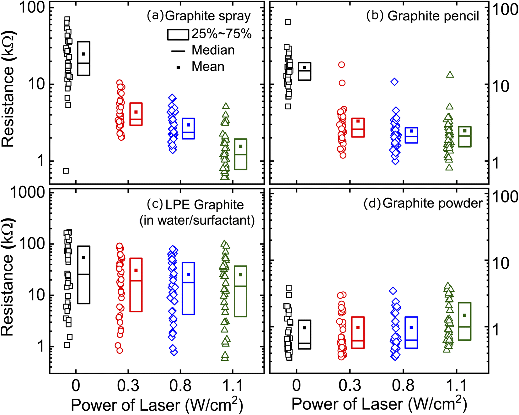 | ||
| Fig. 3 Laser annealing results for various graphite films on standard copy paper. The data points represent individual devices measured. The box plot to the right of a set of data points shows the statistics for that set. The two-terminal resistance is plotted as a function of the laser power density for devices created using spray-on graphite (a), a graphite pencil (b), liquid-phase exfoliated (LPE) graphite in a water/surfactant solution (c), and powder graphite drawn on paper (d). | ||
We attribute the main differences between the laser-induced resistance drop in the films to the diverse nature of the foreign species that hampers the flake-to-flake contact in the graphite film network. In the case of pure graphite, where no impurities are expected to be present in between the flakes, one would in fact expect no improvement upon laser annealing. Moreover, we observe that higher laser power even leads to an increase of resistance indicating damage of the graphite flakes or the paper substrate. For the films based on LPE graphene solutions, one would expect the presence of water with surfactant or DMF molecules between the graphite flakes. We believe that the laser annealing does not achieve full evaporation of these solvent molecules before reaching the paper damage threshold. For spray coated graphite, on the other hand, iso-propanol is used as propellant gas. The boiling point of iso-propanol is lower than that of water and DMF and laser annealing can remove it rather effectively from the graphite network. In the case of the films based on pencil we believe that the mechanism is slightly different: as wax melts at low temperatures (∼40 °C), laser-annealing can melt the wax within the pencil trace that diffuses and coalesces giving way to areas where the graphite-to-graphite contact is improved.
We also explored the possibility of using the laser-annealing process to make patterns of different resistance on the graphite films. Fig. 4(a) presents a proof-of-concept application of the technique, our research logo laser engraved into graphite on paper. For a more quantitative investigation, we selected two test-patterns: a striped pattern (lines of 2 mm wide laser-treated regions separated by 2 mm of untreated film) and a chess board like pattern (with squares of 3.33 by 3.33 mm2). We then directly probed the spatial variation of the resistance of the film using a home-built setup (Fig. S6†). The sample was mounted on a motorized stage used to scan the sample surface. A manual XYZ linear stage was equipped with a probe consisting of two cantilever shaped spring-loaded copper wires separated by 0.5 mm. The copper wires were lowered until establishing a good contact to the sample. We checked that they were compliant enough to not scratch the samples. Finally, we connected the two copper wires to a source-measure unit, applied a 1 V bias and measured the current flow at every step during the scanning of the sample with the motors. In this way, we obtained a spatial map of the sample resistance.
 | ||
| Fig. 4 Pattern annealing graphite films on paper with a raster scanned laser. (a) Image of the logo pattern created in a graphite film drawn on standard copy paper with a graphite pencil. (b) A stripe patterned graphite film on paper. The left side shows a digital camera image of the film after laser annealing a stripe pattern. The right side shows a spatial current map of the film using our home-built scanning setup. The plot below shows the current as a function of position for the box enclosed by the white dashed line above (averaged over 6 lines). (c) A chess board patterned graphite film on paper. The left side shows a digital camera image of the film after laser annealing a chess board pattern. The right side shows a spatial current map of the film using our home-built scanning setup. The plot below shows the current as a function of position for the box enclosed by the white dashed line above (averaged over 10 lines). | ||
Fig. 4(b) and (c) demonstrate how the laser annealing can be effectively used to spatially modulate the resistance of the films based on graphite flakes. In this respect, Fig. 4(b) illustrates the striped pattern device. On the left-hand side, a digital camera image of the device is shown whereas on the right-hand side, a spatial map of the measured current is shown. A clear increase in the current can be appreciated over the regions that were laser annealed. The lower panel in Fig. 4(c) depicts a 1D plot (averaged over 6 lines) of the current as a function of position, showing the increase of current at the annealed stripes. Fig. 4(c) shows the same data set for the chess board like pattern and again the increase in current can be discerned in the annealed regions. This laser-annealing induced local change in resistance can be useful in applications for integrated circuits where a tunable resistance is required across the circuit.25 Moreover, by exceeding the laser damage threshold one could also use the laser annealing to ‘cut’ through the conductive films to isolate different electrical pads.26
We have presented a method to anneal graphite films on paper and polycarbonate. In contrast to conventional high temperature annealing, the proposed technique is derived from fast raster scanning of a high-powered laser to rapidly anneal the films without damaging the underlying sensitive substrates. Significantly, our annealing technique decreases the resistance of spray-on graphite film devices by 16× (from 25.0 kΩ to 1.6. kΩ). An improvement in graphite pencil fabricated films is found as well (from 16.5 kΩ to 2.5 kΩ). Using our technique, we also demonstrate the ability to spatially change the resistance of the film. A home-built scanning system attests for the conductance changes in the patterns written on the film surface. More importantly, our approach is a safe alternative to high temperature annealing for spray-on, drawn, printed, and abrasion fabricated films on sensitive substrates. We anticipate the widespread utilization of this technique to other material films on sensitive substrates for ubiquitous electronics.
Materials and methods
Liquid phase exfoliation with water/surfactant mixture
Sigma Aldrich flake graphite, +100 mesh; Sigma-Aldrich Sodium Cholate Hydrate (≥99%) used as received. Exfoliation Procedure Exfoliation was undertaken based on previous publications.27 Two centrifuge tubes each containing 20 mL mixtures of 15 mg mL−1 graphite and 4 mg mL−1 sodium cholate were sonicated in a bath sonicator (Branson CPX2800-E) for one hour. The dispersions were centrifuged at 6000 rpm (rcf = 3820 × g) for 2 hours and the supernatant was removed. The washed graphite was dried before 20 mL sodium cholate solution (2 mg mL−1) was added to each tube and sonicated for ten hours. To separate different fractions cascade centrifugation was used, centrifuging for two hours at every speed and isolating fractions that were stable between 100–400 g and 6000–30000 g.
Liquid phase exfoliation with DMF
Commercially available graphite powder (micro graphite, 4my 995 from ProGraphite shop) and dimethylformamide (DMF, Sigma Aldrich, ≥99.8%) were used. For the exfoliation, graphite powder was suspended in DMF (1 mg mL−1) and sonicated by probe sonication (Mxmoonant Ultrasonic Homogenizer) for 60 min at 50% power (pulse of 8 s on and 2 s off). The temperature was controlled by a water-ice bath and maintained the dispersion at about 10 °C during sonication.Conflicts of interest
There are no conflicts of interest to declare.Acknowledgements
This work received funding from the European Research Council (ERC) under the European Union's Horizon 2020 Research and Innovation Program (grant agreement no. 755655, ERC-StG 2017 project 2D-TOPSENSE), the Ministry of Science and Innovation (Spain) through the project PID2020-115566RB-I00. AC-G. AMA-E and AN extend their sincere appreciation to the Distinguished Scientist Fellowship Program (DSFP) at King Saud University for funding of this work.References
- K. S. Novoselov, et al., Electric Field Effect in Atomically Thin Carbon Films, Science, 2004, 306, 666–669 CrossRef CAS PubMed.
- A. C. Ferrari, et al., Science and technology roadmap for graphene, related two-dimensional crystals, and hybrid systems, Nanoscale, 2015, 7, 4598–4810 RSC.
- Y. Lee, et al., Wafer-Scale Synthesis and Transfer of Graphene Films, Nano Lett., 2010, 10, 490–493 CrossRef CAS.
- S. Bae, et al., Roll-to-roll production of 30-inch graphene films for transparent electrodes, Nat. Nanotechnol., 2010, 5, 574–578 CrossRef CAS PubMed.
- Y. Hernandez, et al., High-yield production of graphene by liquid-phase exfoliation of graphite, Nat. Nanotechnol., 2008, 3, 563–568 CrossRef CAS PubMed.
- J. N. Coleman, Liquid-Phase Exfoliation of Nanotubes and Graphene, Adv. Funct. Mater., 2009, 19, 3680–3695 CrossRef CAS.
- A. Ciesielski and P. Samorì, Graphene via sonication assisted liquid-phase exfoliation, Chem. Soc. Rev., 2014, 43, 381–398 RSC.
- J. Shen, et al., Liquid Phase Exfoliation of Two-Dimensional Materials by Directly Probing and Matching Surface Tension Components, Nano Lett., 2015, 15, 5449–5454 CrossRef CAS PubMed.
- T. Carey, et al., Fully inkjet-printed two-dimensional material field-effect heterojunctions for wearable and textile electronics, Nat. Commun., 2017, 8, 1202 CrossRef PubMed.
- G. Eda, G. Fanchini and M. Chhowalla, Large-area ultrathin films of reduced graphene oxide as a transparent and flexible electronic material, Nat. Nanotechnol., 2008, 3, 270–274 CrossRef CAS PubMed.
- F. J. Tölle, M. Fabritius and R. Mülhaupt, Emulsifier-Free Graphene Dispersions with High Graphene Content for Printed Electronics and Freestanding Graphene Films, Adv. Funct. Mater., 2012, 22, 1136–1144 CrossRef.
- L. Huang, Y. Huang, J. Liang, X. Wan and Y. Chen, Graphene-based conducting inks for direct inkjet printing of flexible conductive patterns and their applications in electric circuits and chemical sensors, Nano Res., 2011, 4, 675–684 CrossRef CAS.
- F. Torrisi, et al., Inkjet-Printed Graphene Electronics, ACS Nano, 2012, 6, 2992–3006 CrossRef CAS PubMed.
- T. S. Tran, N. K. Dutta and N. R. Choudhury, Graphene inks for printed flexible electronics: graphene dispersions, ink formulations, printing techniques and applications, Adv. Colloid Interface Sci., 2018, 261, 41–61 CrossRef CAS PubMed.
- Y. Gao, W. Shi, W. Wang, Y. Leng and Y. Zhao, Inkjet Printing Patterns of Highly Conductive Pristine Graphene on Flexible Substrates, Ind. Eng. Chem. Res., 2014, 53, 16777–16784 CrossRef CAS.
- E. B. Secor, P. L. Prabhumirashi, K. Puntambekar, M. L. Geier and M. C. Hersam, Inkjet Printing of High Conductivity, Flexible Graphene Patterns, J. Phys. Chem. Lett., 2013, 4, 1347–1351 CrossRef CAS PubMed.
- H. J. Hwang, Y. Lee, C. Cho and B. H. Lee, Facile process to clean PMMA residue on graphene using KrF laser annealing, AIP Adv., 2018, 8, 105326 CrossRef.
- Z. Wan, et al., Laser-Reduced Graphene: Synthesis, Properties, and Applications, Adv. Mater. Technol., 2018, 3, 1700315 CrossRef.
- S. A. Moshkalev, et al., Formation of reliable electrical and thermal contacts between graphene and metal electrodes by laser annealing, Microelectron. Eng., 2014, 121, 55–58 CrossRef CAS.
- S. Majee, et al., Highly Conductive Films by Rapid Photonic Annealing of Inkjet Printable Starch–Graphene Ink, Adv. Mater. Interfaces, 2022, 9, 2101884 CrossRef CAS.
- M. C. Sousa and J. W. Buchanan, Observational Models of Graphite Pencil Materials, Comput. Graph. Forum., 2000, 19, 27–49 CrossRef.
- X. Zheng, et al., The Raman redshift of graphene impacted by gold nanoparticles, AIP Adv., 2015, 5, 057133 CrossRef.
- K. Kumar, Y.-S. Kim and E.-H. Yang, The influence of thermal annealing to remove polymeric residue on the electronic doping and morphological characteristics of graphene, Carbon, 2013, 65, 35–45 CrossRef CAS.
- S. J. Hong, et al., Verification of electron doping in single-layer graphene due to H2 exposure with thermoelectric power, Appl. Phys. Lett., 2015, 106, 142110 CrossRef.
- Y. Sui, et al., Tunable resistivity in ink-jet printed electrical structures on paper by plasma conversion of particle-free, stabilizer-free silver inks, J. Vac. Sci. Technol., A, 2018, 36, 051302 CrossRef.
- V. B. Nam, T. T. Giang, S. Koo, J. Rho and D. Lee, Laser digital patterning of conductive electrodes using metal oxide nanomaterials, Nano Convergence, 2020, 7, 23 CrossRef CAS PubMed.
- C. Backes, et al., Guidelines for Exfoliation, Characterization and Processing of Layered Materials Produced by Liquid Exfoliation, Chem. Mater., 2017, 29, 243–255 CrossRef CAS.
Footnote |
| † Electronic supplementary information (ESI) available. See https://doi.org/10.1039/d2na00557c |
| This journal is © The Royal Society of Chemistry 2022 |