
 Open Access Article
 This Open Access Article is licensed under a Creative Commons Attribution-Non Commercial 3.0 Unported Licence
Effects of low work-function lanthanum oxides on stable electron field emissions from nanoscale emitters
Wataru
Hayami
 *a,
Shuai
Tang†
b,
Jie
Tang
b and
Lu-Chang
Qin
c
*a,
Shuai
Tang†
b,
Jie
Tang
b and
Lu-Chang
Qin
c
aInternational Center for Materials Nanoarchitectonics, National Institute for Materials Science, Tsukuba, Ibaraki 305-0044, Japan. E-mail: HAYAMI.Wataru@nims.go.jp
bCenter for Green Research on Energy and Environmental Materials, National Institute for Materials Science, Tsukuba, Ibaraki 305-0047, Japan
cDepartment of Physics and Astronomy, The University of North Carolina at Chapel Hill, Chapel Hill, NC 27599-3255, USA
First published on 11th October 2022
Abstract
Nanoscale electron field emitters are known to produce more stable electron emissions than conventional emitters. This has been attributed to size effects; nanoscale emitters can operate with a small emission current and a low extraction voltage, which reduces the bombardment of residual gas ions on the emitter tip. However, our experiments discovered that nanoscale LaB6 emitters had extremely stable emissions, suggesting that chemical effects are present in addition to size effects. This suggests that during operations, a material other than LaB6 may be deposited on the surface of the tip to enhance the stability of emissions. Therefore, we searched for possible materials theoretically within the La–B–O ternary system and found that lanthanum oxides (LaO) and oxygen-deficient La2O3 (La2O3−x) had good electrical conductivity and a low work function comparable to that of LaB6. These lanthanum oxides are chemically less reactive to residual gases than LaB6. Thus, if they are present on the LaB6 surface, they could stabilize electron emissions without diminishing the emission performance. These findings suggest that lanthanum oxides could be used for electron field emitters.
1. Introduction
Electron guns have been used for decades in various instruments, including cathode-ray tubes, electron microscopes, and electron-beam lithography systems. They can be classified into the following types of electron emissions: thermionic emissions (TE), Schottky emissions (SE), thermal field emissions (TFE), and cold field emissions (CFE). Electron source materials are chosen to correspond to each emission type, for instance, tungsten (W) for TE and CFE, LaB6 and CeB6 for TE, and tungsten coated with zirconium oxide (W/ZrO) for SE.1–3Currently, W is used for the emitter tip of CFE electron guns because it can be processed to dimensions less than 100 nm, which is necessary to create a high electric field (>109 V m−1) and produce a fairly constant emission current. Many studies have been conducted to find electron source materials with superior emission properties, for example, single-atom tips,4–6 carbon nanotubes,7–9 and etched sharp tips of borides,10–26 carbides,27–39 and nitrides.40–46
In particular, LaB6 has been studied repeatedly since the 1970s because its low work function (WF) (2.1–2.6 eV) and chemical stability made it ideal as a TE emitter. Earlier studies of CFE from a LaB6 tip found that the emission current was not sufficiently stable and decayed after several minutes.10 Since around the year 2000, advanced technologies have been implemented to fabricate nanoscale LaB6 emitters.15–26 A LaB6 nanowire with a thickness of less than 100 nm has been synthesized by chemical vapor deposition (CVD).21 When applied to an electron emitter, the LaB6 nanowire produced a stable CFE.22–24 Notably, the emission current exhibited extreme stability without decay for over tens of hours.24 Furthermore, a LaB6 nanoneedle created by focused ion beam (FIB) milling demonstrated a higher degree of stability than nanowires and greatly exceeded the performance of the W emitter.25 The LaB6 nanoneedle emitter was assembled in a TEM and was capable of long-term stable (<1%/100 h) atomic imaging, which has never been achieved by other CFE electron sources.26
The reason for the high current stability is attributed to the following:1 (i) to achieve the same probe current, the total emission current for the nanoscale emitter is several orders of magnitude smaller than that of the conventional emitter, which reduces the generation of residual gas ions and consequently reduces the ion bombardment on the emitter tip; (ii) the lower extraction voltage for the nanoscale emitter is also advantageous for reducing residual gas ions and damage caused by the ion bombardment. In addition, we proposed another possible factor in our previous study;25 (iii) the electric current density in the apex region becomes so intense (∼106 A cm−2) that electrons provide kinetic momentum to the adatoms on the surface, inducing an atomic flow toward the apex (electromigration) and eventually enhancing the desorption rate of the adatoms.
The above findings are size effects that apply to all nanoscale emitters. In addition to size effects, it appeared in our experiments24,25 that chemical effects might also have been observed on the nanoscale LaB6 emitters, that is, a material other than LaB6 was deposited on the surface, and it enhanced the current stability. We conceived this idea after noticing that the energy-dispersive X-ray spectroscopy (EDS) image of the nanoneedle tip appeared to show a reduction of boron atoms on the surface layers.25
Although the EDS analysis suggested the presence of chemical effects, it was not decisive enough to reach this conclusion. Therefore, in this study, we theoretically investigated whether chemical effects occur on the nanoscale LaB6 tip and attempted to identify the materials covering the surface. The study was conducted for the most part using first-principles calculations and molecular dynamics (MD) simulations. We extensively searched for materials in the phase diagram that satisfied the required conditions for stabilizing the emission current.
2. Calculation methods
The calculations of the electronic structures and Car–Parrinello MD simulations were conducted using the Quantum ESPRESSO code,47,48 based on density functional theory with plane waves and pseudopotentials. The ultrasoft pseudopotentials49 were adopted from the library of Quantum ESPRESSO.50 The generalized gradient approximation functional of Perdew, Burke, and Ernzerhof was employed.51 An energy cut-off of 80 Ry for plane waves and 560 Ry for electron density were sufficient to provide the convergence of the total energy. The DOS and WF were calculated following the optimization of the lattice parameters and the atomic structures using Monkhorst–Pack k-point sampling52 with an 8 × 8 × 8 mesh for the unit cell. The calculated lattice parameters were within an error of 1% from the corresponding experimental values.Slab models were used for the WF calculations and MD simulations, which comprised several atomic layers separated by a vacuum layer of 15 Å. The WF ϕ was estimated using the following formula:53
| ϕ = Vvac − Ef | (1) |
3. Results and discussion
According to the EDS analysis,25 the atomic elements detected on the outermost surface of the LaB6 emitter were La, B, and O. Therefore, we searched for materials consisting of these three elements. Since hydrogen is not detected by EDS, the possibility of the synthesis of hydroxides cannot be excluded. This is discussed in Section 3.5. As there appear to be no experimental phase diagrams available for the ternary La–B–O system, we calculated the theoretical phase diagram using the Open Quantum Materials Database (OQMD).54 The calculation method for judging the stability of compounds was based on DFT + U55 and the Quickhull algorithm.56The results are shown in Fig. 1, where stable and unstable (metastable) compounds are represented by green and red circles, respectively. There are some other unstable compounds omitted from the figure. La3BO6, denoted by the yellow circle, did not appear in this calculation although its existence has been experimentally confirmed.57–59 Therefore, it is added to Fig. 1. As the stable compounds are aligned along the lines of B–La, La–O, B–O, and B2O3–La2O3 binary systems, we searched for possible materials covering the LaB6 tip along these binary lines.
 | ||
| Fig. 1 Calculated ternary phase diagram of the La–B–O system. Green and red circles denote stable and unstable (metastable) compounds, respectively. See the text for the yellow circle (La3BO6). | ||
3.1. Lanthanum borides
First, we considered LaB4 in the B–La system as a potential covering material because of the following: (i) it is metallic;60 (ii) it has been observed on oxidized LaB6 surfaces;61–63 (iii) it is structurally similar to LaB6.64 The covering materials must be conductive; otherwise, they will obstruct electron emissions from the surfaces. LaB4 has a tetragonal crystal structure, including octahedral B6 clusters, like LaB6. By analogy with LaB6,65 we expected that LaB4 would have a lower WF when its surface was terminated by a La layer, and we calculated the WF of the La-terminated LaB4 (001) surface using a slab model of (1 × 1 × 6) unit cells separated by a 15 Å space. The result showed that the WF of the La-terminated surface was about 3.2 eV, and that of the opposite surface, terminated by a B layer, was about 4.5 eV. In contrast to our expectations, the WF of LaB4 was much higher than that of LaB6, meaning that LaB4 would diminish the performance of the LaB6 emitter if present on the surface. Consequently, LaB4 could not be a candidate material.3.2. Lanthanum monoxide LaO
Except for LaB4, no stable materials in the phase diagram (Fig. 1) are as conductive as LaB6. However, LaO (NaCl structure), though judged to be unstable, has been reported to be metallic.66–68 It was synthesized for the first time under high pressure66 and recently as a thin film on substrates.67,68 Thin films of high-pressure phases sometimes appear because of the stress applied by the interface. Notably, LaO was also observed in the LaB6 oxidation experiment.69 For these reasons, we anticipated that LaO could be a covering material, and we calculated the electronic density of states (DOS) and the WF.The DOS of LaO shown in Fig. 2 indicates that it is metallic, which is consistent with previous experimental and theoretical results.66–68 The states at the Fermi level originate mostly from the d-orbitals of the La atoms. The WF of the LaO(001) surface was calculated employing the slab model shown in the inset of Fig. 2. The model consisted of six layers of LaO separated by a 15 Å space fully optimized before the WF calculation. The calculated WF was approximately 2.3 eV, which is very close to that of LaB6. Therefore, LaO does not greatly diminish electron emissions even if it covers the LaB6 surface. It was not previously known that LaO has a WF as low as that of LaB6. LaO could be applied to electron emitters if it generates stable electron emissions.
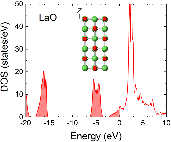 | ||
| Fig. 2 DOS of LaO with the Fermi level set to zero. The inset depicts a slab model for the WF calculation. | ||
If LaO is chemically stable and can cover the LaB6 emitter, it would stabilize electron emissions. To investigate the chemical stability of LaO, we conducted Car–Parrinello MD simulations of gas molecule adsorption under the operating conditions of the emitter. For the (001) surfaces of LaB6 and LaO, slab models of (2 × 2 × 3) unit cells were employed (Fig. 3), on which the gas molecules H2, O2, H2O, and CO were initially placed at a height of 4 Å from the surface. Although the operating temperature of the emitter tip is uncertain, it should be slightly higher than room temperature and was assumed to be 500 K in the simulations. The actual temperature would not exceed this because the energy dispersion of the emitted electron beam was small.25 The duration of the simulations was 1.5 to 3.0 ps.
 | ||
| Fig. 3 Snapshots of MD simulations of H2O adsorption on LaB6(001) (top left) and on LaO(001) (top right); O2 adsorption on LaB6(001) (bottom left) and on LaO(001) (bottom right). O atoms in the LaO crystal and those from the adsorbents are denoted by red and orange spheres, respectively. | ||
In the case of H2O adsorption, the H2O molecule spontaneously dissolved and was chemisorbed on LaB6(001) (Fig. 3, top left) with the H atom on a B atom and the OH on a La atom. In contrast, the H2O molecule did not immediately dissolve on LaO(001) (top right).
With regard to O2 adsorption, the O2 molecule was dissolved and chemisorbed on LaB6(001) (Fig. 3, bottom left) with O atoms on B atoms when the WF was increased by 0.13 eV. Similarly, the O2 molecule was dissolved on LaO(001), but the O atoms seemed to be absorbed into the bulk (bottom right). This suggests that LaO spontaneously transforms into the more stable La2O3 phase when plenty of O atoms are supplied. Since the adsorbed O atoms are far fewer than the bulk O atoms, LaO does not transform into La2O3 in the present case. The WF of LaO(001) hardly increased upon O2 adsorption, probably because the dissolved O atoms did not remain on the surface, and the DOS of the bulk underwent little change with the additional O atoms. As for H2 and CO adsorptions, the H2 molecule was not adsorbed on LaB6(001) or LaO(001), and the CO molecule was adsorbed but not dissolved on these surfaces. The observed inactivity of H2 on the LaB6 surfaces was consistent with experimental results.70
Although the duration time and the initial conditions were limited, the results of the MD simulations suggest that the LaO(001) surface was chemically as stable as, or slightly more stable than, the LaB6(001) surface. The LaO(001) surface was not resistant to oxidation; however, it would appear to be resistant in practice because the WF was hardly influenced by oxidation. Consequently, LaO is a candidate for the materials covering the LaB6 tip.
3.3. Lanthanum oxides La2O3 and LaO2
Along with LaO, a large amount of La2O3 was observed in the LaB6 oxidation experiment.69 This is to be expected because La2O3 is the most stable phase in the La–O binary system (Fig. 1). La2O3 is a potential high-k material that can be used for semiconductor devices.71–74 When it is applied to gate insulators, the leak current becomes a problem in the presence of oxygen vacancies, even at low temperatures. The vacancies are supposed to work as donors and induce the electric current of Poole–Frenkel types71,73,74 and space-charge limited types.73,74Having adequate electrical conductivity, La2O3 with O vacancies (La2O3−x) would not obstruct emissions from the LaB6 tip and would serve as LaO if the WF is sufficiently low. The DOS and WF calculations for La2O3−x require attention because of its polymorphism. La2O3 of hexagonal (space group P![[3 with combining macron]](https://www.rsc.org/images/entities/char_0033_0304.gif) m1), monoclinic (C2/m), and cubic (Ia) structures have been observed in the LaB6 oxidation experiment.69 With the inclusion of another reported cubic phase (LaO1.5, Imm),75 we investigated the electronic structures of La2O3−x in these four crystal structures.
m1), monoclinic (C2/m), and cubic (Ia) structures have been observed in the LaB6 oxidation experiment.69 With the inclusion of another reported cubic phase (LaO1.5, Imm),75 we investigated the electronic structures of La2O3−x in these four crystal structures.
In the cubic (Imm) phase, the oxygen sites are split and randomized, as such a structure cannot be realized using a single unit cell. An approximate structure model was constructed employing a (2 × 2 × 2) cell with the oxygen positions randomized by MD simulations and annealing. There is an additional hexagonal phase (P63/mmc), but it is merely a variant of the hexagonal (Pm1) phase with split oxygen sites and, therefore, was excluded from the calculations. There are several oxygen sites in hexagonal and monoclinic structures. To create vacancies, an O atom was removed from each structure to attain the lowest total energy. For the hexagonal phase, an O atom coordinated with six La atoms was removed, and for the monoclinic phase, an O atom coordinated with five La atoms was removed.
Fig. 4 shows the DOS of hexagonal La2O3 (no vacancies) and four polymorphs of La2O3−x (with vacancies) mentioned above. The concentrations of O vacancies were adjusted to about 5% in the calculations, depending on the number of atoms in the unit cell. In all the structures, it was observed that O vacancies generated new states near the bottom of the conduction band, and the Fermi level laid at the top of the new states. The band gaps from the new states to the conduction band were less than 0.5 eV, so the materials practically became conductive by the thermal excitation of the electrons. The values of the band gap were in good agreement with experimental values.73 The mobility of electrons is determined by the dispersion relation of the conduction band. The lower part of the conduction band consists of 5d and 6s orbitals of La atoms and the dispersion relation is similar to that of LaB6, suggesting the same degree of electron mobility. As the vacancy concentrations increase, it is likely that the materials become more conductive and the DOS approaches that of LaO (Fig. 2).
 | ||
| Fig. 4 Electronic DOS of La2O3 and La2O3−x. (a) no defects, (b) hexagonal with x = 0.125, (c) monoclinic with x = 0.167, (d) cubic (Ia) with x = 0.125, and (e) cubic (Imm) with x = 0.125. The insets depict the surfaces on which the WF was calculated. | ||
It is laborious to calculate the WF for all the crystal surfaces. Empirically, in ionic crystals, neutral surfaces tend to appear on which the total charge of cations and anions is zero. Neutral surfaces do not have electric dipoles perpendicular to the surface, which implies that the work functions of neutral surfaces are determined mainly by the electronic structure of the bulk rather than by the Miller indices. Based on this rule, we calculated the WF on the neutral surfaces chosen, as illustrated in the insets of Fig. 4: the (11![[2 with combining macron]](https://www.rsc.org/images/entities/char_0032_0304.gif) 0) surface for the hexagonal crystal, (010) for the monoclinic, (110) for the cubic (Ia), and (001) for the cubic (Imm). The results summarized in Table 1 show that the WFs of these surfaces were around 2.0 eV, close to that of LaB6 and LaO. It should be noted that these values agree well with the electron affinity of La2O3 (2 eV),72 which corresponds to the energy difference between the vacuum level and the bottom of the conduction band. The good agreement between the calculated and experimental values affirms the validity of the choice of the neutral surfaces. La2O3−x, with such a low WF, would not diminish the emission performance of the LaB6 tip.
0) surface for the hexagonal crystal, (010) for the monoclinic, (110) for the cubic (Ia), and (001) for the cubic (Imm). The results summarized in Table 1 show that the WFs of these surfaces were around 2.0 eV, close to that of LaB6 and LaO. It should be noted that these values agree well with the electron affinity of La2O3 (2 eV),72 which corresponds to the energy difference between the vacuum level and the bottom of the conduction band. The good agreement between the calculated and experimental values affirms the validity of the choice of the neutral surfaces. La2O3−x, with such a low WF, would not diminish the emission performance of the LaB6 tip.
| Material | WF (eV) | Surface |
|---|---|---|
| LaO | 2.3 | (001) |
| La2O3−x hexagonal | 1.8 | (110) |
| La2O3−x monoclinic | 2.0 | (010) |
| La2O3−x cubic (Ia) |
1.9 | (110) |
| La2O3−x cubic (Imm) |
2.1 | (001) |
| La(OH)3−x | 1.9 | (0001) |
| LaB6 | 2.3 | (001) |
| LaB4 | 3.2 | (001) |
To investigate the chemical stability of La2O3−x, as was done for LaO (Fig. 3), MD simulations were conducted with H2O, O2, H2, and CO molecules on the (110) surface of hexagonal La2O3−x (Fig. 4b inset). The conditions of the MD simulations were the same as for LaO (500 K and 3 ps). As a result, these molecules did not dissolve on the surface within the simulation time. Since the electronic states of other polymorphs of La2O3−x are very similar to the hexagonal one, the results indicate that the La2O3−x surfaces are more stable than the LaB6(001) and LaO(001) surfaces. Taking the low WF and high chemical stability into consideration, La2O3−x can be a covering material for the LaB6 tip and may function as an electron emitter.
According to the calculated phase diagram (Fig. 1), LaO2 was classified as being in a stable phase. However, there have been no experimental reports on the synthesis of LaO2; there is only a theoretical prediction of it.76 We investigated the electronic structure of LaO2, based on the atomic structure provided by Marques et al.76,77 When the structure was optimized, it appeared to be locally stable. The calculated DOS showed that LaO2 was an insulator with a band gap of approximately 3 eV. When an O vacancy was introduced, it remained an insulator without any change in the value of the band gap. This is probably because O atoms are redundant in LaO2 to complete the ionic bonds with the La atoms. Since both La2O3 and LaO2 are insulators, all compounds between them (LaOx, [1.5 ≤ x ≤ 2.0]) are very likely to be insulators and would obstruct emissions from the LaB6 tip.
3.4. Lanthanum borates, metaborates, and boron oxides
By analogy with La2O3, we considered that borates, metaborates, and boron oxides in the phase diagram (Fig. 1) might possibly have the same properties as La2O3, and we calculated the electronic structures of LaBO3, LaB3O6, B2O3, and B6O in the presence of O vacancies. La3BO6, denoted by the yellow circle in Fig. 1, was excluded from the considerations because its crystal structure is unknown. Its properties will be inferred from the results for LaBO3 and LaB3O6. Regarding LaB3O6, it has two O sites, one coordinated with a La atom and the other with two La atoms. An O atom was removed from the former site to reduce the total energy.Fig. 5 shows the calculated DOS of these materials with O vacancies. For LaBO3−x (a), LaB3O6−x (b), and B2O3−x (c), the defect levels (blue arrows) appear in the middle of the original band gap. For B6O1−x (d), an unoccupied defect level is located at the bottom of the conduction band. In the DOS of B2O3−x (c), LaB3O6−x (b), and LaBO3−x (a), the defect level shifts upward as the composition approaches La2O3−x on the B2O3–La2O3 line (Fig. 1). This is consistent with the results for La2O3−x, where the defect levels were at the bottom of the conduction band (Fig. 4). Since La3BO6 is located at the midpoint between LaBO3 and La2O3 in the phase diagram (Fig. 1), it is reasonable to infer that La3BO6 with O vacancies still had a band gap. Thus, the La borates, metaborates, and boron oxides cannot be conductive even in the presence of O vacancies and are unlikely to cover the LaB6 tip.
 | ||
| Fig. 5 Electronic DOS of (a) LaBO3−x, (b) LaB3O6−x, (c) B2O3−x, and (d) B6O1−x. The blue arrows indicate the defect levels. The Fermi level is set to zero. | ||
3.5. Lanthanum hydroxide La(OH)3
Except for the ternary compounds presented in Fig. 1, it is known that La(OH)3 is produced from La2O3 by a simple hydration reaction.78 We therefore investigated the possibility that La(OH)3 might become conductive when defects are introduced. The DOS of La(OH)3 was calculated with OH vacancies instead of O vacancies because O and H atoms are paired in the structure. The DOS of La(OH)3−x (Fig. 6) is similar to that of La2O3−x (Fig. 4), where the defect levels appear at the bottom of the conduction band, which makes La(OH)3−x as conductive as La2O3−x. The WF of La(OH)3−x calculated on the neutral (0001) surface (Fig. 6 inset) was approximately 1.9 eV, which is comparable to that of La2O3−x and LaO (Table 1). Thus, La(OH)3−x could be a covering material for the LaB6 tip. However, La(OH)3 dehydrates at 330 °C and converts to La2O3,79 so in this case, La(OH)3 does not need to be considered because the emitter tip was cleaned by flash heating at about 800 °C.25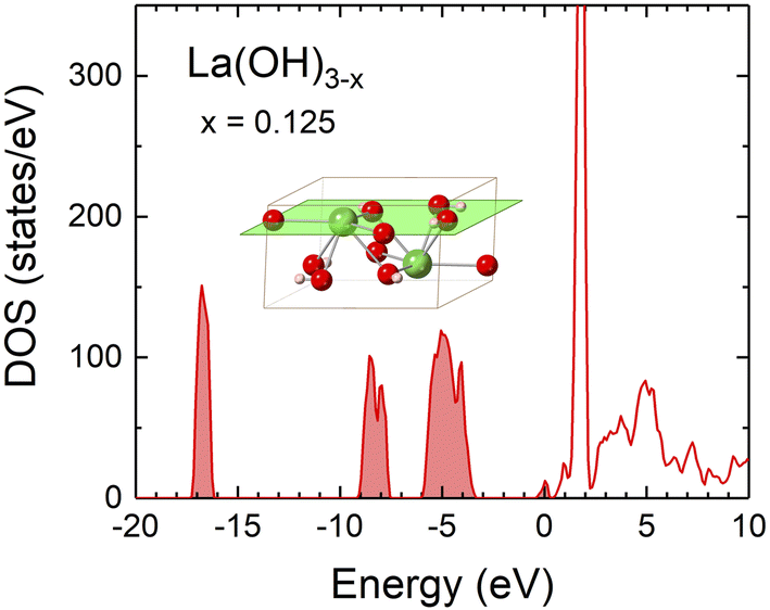 | ||
| Fig. 6 Electronic DOS of La(OH)3−x with x = 0.125. The Fermi level is set to zero. The inset depicts the (0001) surface on which the WF was calculated. | ||
3.6. Synthesis mechanism of LaO and La2O3
Our theoretical studies found that LaO and La2O3−x could enhance the chemical stability of the LaB6 emitter without degrading the emission performance. If these La oxides were present on the LaB6 surface, we can surmise their synthesis mechanism from the various experiments we describe below.When a LaB6 crystal is exposed to an oxygen atmosphere, O2 molecules are dissociatively adsorbed on the surface even at room temperature.80–85 When the crystal is heated in an oxygen atmosphere to around 500–700 °C, the surface starts to be oxidized to yield LaO, La2O3, B2O3, LaBO3, LaB3O6, and La3BO6 on the macroscopic scale.69,86 However, in our experimental conditions,25 the LaB6 tip was heated for cleaning in an ultrahigh vacuum, where the desorption processes are as significant as the oxidation processes. The oxide layers would then be limited to several atomic layers. In the thermal desorption experiments,81,82 B oxides in the forms of BO and B2O2 began to desorb at temperatures around 1000 K (727 °C), and La oxides in the form of LaO desorbed at higher temperatures of around 1400 K (1127 °C). At about 1500 °C, the LaB6 surface became clean.11 In our experiments,25 the LaB6 tip was heated at a moderate temperature of about 800 °C, which would incidentally have B oxides desorb and La oxides remain on the surface.
Regarding La borates and metaborates (LaBO3, LaB3O6, and La3BO6) that have been synthesized in an oxygen atmosphere,69,86 it is uncertain whether they can be synthesized under oxygen-depleted conditions. Considering the fact that these materials are synthesized at temperatures (∼900 °C) slightly higher than the temperature at which boron oxides BO and B2O2 are desorbed in a vacuum (727 °C),81,82 it seems unlikely that La borates and metaborates are preferably synthesized on the LaB6 surface in an ultrahigh vacuum.
4. Conclusions
In order to examine possible chemical effects on LaB6 nanoscale emitters, we searched for materials that could cover the emitter tip to stabilize electron emissions during long operating times. Extensive studies, based on the ternary phase diagram of the La–B–O system, showed that LaO and La2O3−x could serve as the covering material. Compared with LaB6, these materials have higher chemical stability against typical residual gases (H2, O2, H2O, and CO) and have an equivalently low WF, which enables the emitter to maintain excellent emission performance. It should be noted that these chemical effects can coexist with size effects. It is presumed that flash heating at a moderate temperature of around 800 °C played a crucial role in the LaB6 tip having LaO and/or La2O3−x layers, where B oxides are selectively desorbed and La oxides remain on the surface. It was recognized for the first time that LaO and La2O3−x have such a low WF that they could be used for electron emitters.Author contributions
W. H. conducted theoretical calculations and wrote the initial draft. S. T. performed the experiments and provided extensive comments on the manuscript. J. T. and L.-C. Q. managed the entire research project. All authors contributed to the discussion.Conflicts of interest
There are no conflicts to declare.Acknowledgements
Part of this work was supported by the Nanostructural Characterization Group of the NIMS Electron Microscopy Analysis Station.References
- L. W. Swanson and G. A. Schwind, Adv. Imaging Electron Phys., 2009, 159, 63–100 CrossRef CAS.
- L. W. Swanson and G. A. Schwind, in Handbook of Charged Particle Optics, ed. J. Orloff, CRC Press, New York, 2nd edn, 2008, ch. 1, pp. 1–28 Search PubMed.
- R. G. Forbes, in Handbook of Charged Particle Optics, ed. J. Orloff, CRC Press, New York, 2nd edn, 2008, ch. 3, pp. 87–128 Search PubMed.
- N. D. Lang, A. Yacoby and Y. Imry, Phys. Rev. Lett., 1989, 63, 1499–1502 CrossRef CAS PubMed.
- H. Kuo, I. Hwang, T. Fu, J. Wu, C. Chang and T. Tsong, Nano Lett., 2004, 4, 2379–2382 CrossRef CAS.
- T. Ishikawa, T. Urata, B. Cho, E. Rokuta and C. Oshima, Appl. Phys. Lett., 2007, 90, 143120 CrossRef.
- W. A. de Heer, A. Châtelain and D. Ugarte, Science, 1995, 270, 1179–1180 CrossRef CAS.
- Y. Saito, K. Hamaguchi, K. Hata, K. Uchida, Y. Tasaka, F. Ikazaki, M. Yumura, A. Kasuya and Y. Nishina, Nature, 1997, 389, 554–555 CrossRef CAS.
- G. Zhao, J. Zhang, Q. Zhang, H. Zhang, O. Zhou, L.-C. Qin and J. Tang, Appl. Phys. Lett., 2006, 89, 193113 CrossRef.
- R. Shimizu, Y. Kataoka, T. Tanaka and S. Kawai, Jpn. J. Appl. Phys., 1975, 14, 1089–1090 CrossRef CAS.
- M. Futamoto, S. Hosoki, H. Okano and U. Kawabe, J. Appl. Phys., 1977, 48, 3541–3546 CrossRef CAS.
- S. Zaima, M. Sase, H. Adachi, Y. Shibata, C. Ohshima, T. Tanaka and S. Kawai, J. Phys. D: Appl. Phys., 1980, 13, L47–L49 CrossRef CAS.
- H. Nagata, K. Harada and R. Shimizu, J. Appl. Phys., 1990, 68, 3614–3618 CrossRef CAS.
- K. Harada, H. Nagata and R. Shimizu, J. Electron Microsc., 1991, 40, 1–4 Search PubMed.
- M. Nakamoto and K. Fukuda, Appl. Surf. Sci., 2002, 289–294 CrossRef CAS.
- D. J. Late, M. A. More, D. S. Joag, P. Misra, B. N. Singh and L. M. Kukreja, Appl. Phys. Lett., 2006, 89, 123510 CrossRef.
- H. Liu, X. Zhang, Y. Li, Y. Xiao, W. Zhang and J. Zhang, Appl. Phys. Lett., 2018, 112, 151604 CrossRef.
- G. Singh, R. Bücker, G. Kassier, M. Barthelmess, F. Zheng, V. Migunov, M. Kruth, R. E. Dunin-Borkowski, S. T. Purcell and R. J. D. Miller, Appl. Phys. Lett., 2018, 113, 093101 CrossRef.
- K. Kasuya, T. Kusunoki, T. Hashizume, T. Ohshima, S. Katagiri, Y. Sakai and N. Arai, Appl. Phys. Lett., 2020, 117, 213103 CrossRef CAS.
- S. Tang, J. Tang, Y. Wu, Y. H. Chen, J. Uzuhashi, T. Ohkubo and L. C. Qin, Nanoscale, 2021, 13, 17156–17161 RSC.
- H. Zhang, Q. Zhang, J. Tang and L.-C. Qin, J. Am. Chem. Soc., 2005, 127, 2862–2863 CrossRef CAS PubMed.
- H. Zhang, J. Tang, Q. Zhang, G. Zhao, G. Yang, J. Zhang, O. Zhou and L. C. Qin, Adv. Mater., 2006, 18, 87–91 CrossRef CAS.
- H. Zhang, J. Tang, J. Yuan, J. Ma, N. Shinya, K. Nakajima, H. Murakami, T. Ohkubo and L. C. Qin, Nano Lett., 2010, 10, 3539–3544 CrossRef CAS PubMed.
- H. Zhang, J. Tang, J. Yuan, Y. Yamauchi, T. T. Suzuki, N. Shinya, K. Nakajima and L. C. Qin, Nat. Nanotechnol., 2016, 11, 273–279 CrossRef CAS PubMed.
- S. Tang, J. Tang, J. Uzuhashi, T. Ohkubo, W. Hayami, J. Yuan, M. Takeguchi, M. Mitome and L.-C. Qin, Nanoscale Adv., 2021, 3, 2787–2792 RSC.
- S. Tang, J. Tang, E. Okunishi, Y. Ninota, A. Yasuhara, J. Uzuhashi, T. Ohkubo, M. Takeguchi, J. Yuan and L.-C. Qin, Mater. Today, 2022, 57, 35–42 CrossRef CAS.
- K. Senzaki and Y. Kumashiro, Jpn. J. Appl. Phys., 1974, 13, 289–292 CrossRef.
- H. Adachi, K. Fujii, S. Zaima, Y. Shibata, C. Oshima, S. Otani and Y. Ishizawa, Appl. Phys. Lett., 1983, 43, 702–703 CrossRef CAS.
- K. Fujii, S. Zaima, Y. Shibata, H. Adachi and S. Otani, J. Appl. Phys., 1985, 57, 1723–1728 CrossRef CAS.
- W. A. Mackie, C. H. Hinrichs and P. R. Davis, IEEE Trans. Electron Devices, 1989, 36, 2697–2702 CAS.
- Y. Ishizawa, T. Aizawa and S. Otani, Appl. Surf. Sci., 1993, 67, 36–42 CrossRef CAS.
- M. L. Yu, N. D. Lang, B. W. Hussey and T. H. P. Chang, Phys. Rev. Lett., 1996, 77, 1636–1639 CrossRef CAS PubMed.
- J. Yuan, H. Zhang, J. Tang, N. Shinya, K. Nakajima and L.-C. Qin, Appl. Phys. Lett., 2012, 100, 113111 CrossRef.
- T.-W. Chiu, J. Tang, S. Tang, J. Yuan and L.-C. Qin, Phys. Status Solidi A, 2020, 217, 2000007 CrossRef CAS.
- T.-W. Chiu, J. Tang, S. Tang, J. Yuan and L.-C. Qin, Mater. Today Commun., 2020, 25, 101240 CrossRef CAS.
- T.-W. Chiu, J. Tang, S. Tang, W. Hayami, J. Yuan and L.-C. Qin, Appl. Phys. Lett., 2020, 117, 053101 CrossRef CAS.
- S. Tang, J. Tang, T. W. Chiu, J. Uzuhashi, D. M. Tang, T. Ohkubo, M. Mitome, F. Uesugi, M. Takeguchi and L. C. Qin, Nanoscale, 2020, 12, 16770–16774 RSC.
- S. Tang, J. Tang, T.-W. Chiu, W. Hayami, J. Uzuhashi, T. Ohkubo, F. Uesugi, M. Takeguchi, M. Mitome and L. C. Qin, Nano Res., 2020, 13, 1620–1626 CrossRef CAS.
- W. Hayami, S. Tang, T. W. Chiu and J. Tang, ACS Omega, 2021, 6, 14559–14565 CrossRef CAS PubMed.
- M. Endo, H. Nakane and H. Adachi, Appl. Surf. Sci., 1996, 94/95, 113–116 CrossRef CAS.
- W. K. Lo, J. Vac. Sci. Technol., B: Microelectron. Nanometer Struct.–Process., Meas., Phenom., 1996, 14, 3787 CrossRef CAS.
- M. Nagao, Y. Gotoh, T. Ura, H. Tsuji and J. Ishikawa, J. Vac. Sci. Technol., B: Microelectron. Nanometer Struct.–Process., Meas., Phenom., 1999, 17, 623 CrossRef CAS.
- D. Lee, D. Baik, N. Kang, W. Cho, S. Yoon, T. Kim, H. Hwang, D. Ahn and M. Park, J. Vac. Sci. Technol., B: Microelectron. Nanometer Struct.–Process., Meas., Phenom., 2000, 18, 1085 CrossRef CAS.
- T. Chen, J. Hung, F. Pan, L. Chang, J.-T. Sheu and S. Wu, Electrochem. Solid-State Lett., 2008, 11, K40 CrossRef CAS.
- K. Ikeda, W. Ohue, K. Endo, Y. Gotoh and H. Tsuji, J. Vac. Sci. Technol., B: Microelectron. Nanometer Struct.–Process., Meas., Phenom., 2011, 29, 02B116 CrossRef.
- Y. Tao, Q. Gao, X. Wang, X. Wu, C. Mao and J. Zhu, J. Nanosci. Nanotechnol., 2011, 11, 3345–3349 CrossRef CAS PubMed.
- P. Giannozzi, S. Baroni, N. Bonini, M. Calandra, R. Car, C. Cavazzoni, D. Ceresoli, G. L. Chiarotti, M. Cococcioni, I. Dabo, A. Dal Corso, S. de Gironcoli, S. Fabris, G. Fratesi, R. Gebauer, U. Gerstmann, C. Gougoussis, A. Kokalj, M. Lazzeri, L. Martin-Samos, N. Marzari, F. Mauri, R. Mazzarello, S. Paolini, A. Pasquarello, L. Paulatto, C. Sbraccia, S. Scandolo, G. Sclauzero, A. P. Seitsonen, A. Smogunov, P. Umari and R. M. Wentzcovitch, J. Phys.: Condens. Matter, 2009, 21, 395502 CrossRef PubMed.
- P. Giannozzi, O. Andreussi, T. Brumme, O. Bunau, M. Buongiorno Nardelli, M. Calandra, R. Car, C. Cavazzoni, D. Ceresoli, M. Cococcioni, N. Colonna, I. Carnimeo, A. Dal Corso, S. de Gironcoli, P. Delugas, R. A. DiStasio Jr, A. Ferretti, A. Floris, G. Fratesi, G. Fugallo, R. Gebauer, U. Gerstmann, F. Giustino, T. Gorni, J. Jia, M. Kawamura, H. Y. Ko, A. Kokalj, E. Küçükbenli, M. Lazzeri, M. Marsili, N. Marzari, F. Mauri, N. L. Nguyen, H. V. Nguyen, A. Otero-de-la-Roza, L. Paulatto, S. Poncé, D. Rocca, R. Sabatini, B. Santra, M. Schlipf, A. P. Seitsonen, A. Smogunov, I. Timrov, T. Thonhauser, P. Umari, N. Vast, X. Wu and S. Baroni, J. Phys.: Condens. Matter, 2017, 29, 465901 CrossRef CAS PubMed.
- D. Vanderbilt, Phys. Rev. B: Condens. Matter Mater. Phys., 1990, 41, 7892–7895 CrossRef PubMed.
- Quantum ESPRESSO, http://www.quantum-espresso.org Search PubMed.
- J. P. Perdew, K. Burke and M. Ernzerhof, Phys. Rev. Lett., 1996, 77, 3865–3868 CrossRef CAS PubMed.
- H. J. Monkhorst and J. D. Pack, Phys. Rev. B: Solid State, 1976, 13, 5188–5192 CrossRef.
- W. Liu, W. T. Zheng and Q. Jiang, Phys. Rev. B: Condens. Matter Mater. Phys., 2007, 75, 235322 CrossRef.
- OQMD, The Open Quantum Materials Database, https://www.oqmd.org Search PubMed.
- V. Stevanović, S. Lany, X. Zhang and A. Zunger, Phys. Rev. B: Condens. Matter Mater. Phys., 2012, 85, 115104 CrossRef.
- C. B. Barber, D. P. Dobkin and H. Huhdanpaa, ACM Trans. Math. Softw., 1996, 22, 469–483 CrossRef.
- E. M. Levin, C. R. Robbins and J. L. Waring, J. Am. Ceram. Soc., 1961, 44, 87–91 CrossRef.
- M. G. Zuev, Russ. J. Inorg. Chem., 1998, 43, 1132–1135 Search PubMed.
- S. Sari, F. T. Senberber, M. Yildirim, A. S. Kipcak, S. A. Yuksel and E. M. Derun, Mater. Chem. Phys., 2017, 200, 196–203 CrossRef CAS.
- Z. P. Yin and W. E. Pickett, Phys. Rev. B: Condens. Matter Mater. Phys., 2008, 77, 035135 CrossRef.
- V. A. Lavrenko, L. A. Glebov, Y. S. Lugovskaya and I. N. Frantsevich, Oxid. Met., 1973, 7, 131–139 CrossRef CAS.
- R. F. Voitovich and É. A. Pugach, Poroshk. Metall., 1973, 2, 71–75 Search PubMed.
- D. M. Goebel, Y. Hirooka and T. A. Sketchley, Rev. Sci. Instrum., 1985, 56, 1717–1722 CrossRef CAS.
- K. Kato, I. Kawada, C. Oshima and S. Kawai, Acta Crystallogr., Sect. B: Struct. Crystallogr. Cryst. Chem., 1974, 30, 2933–2934 CrossRef.
- M. Aono, T. Tanaka, E. Bannai, C. Oshima and S. Kawai, Phys. Rev. B: Solid State, 1977, 16, 3489–3492 CrossRef CAS.
- J. M. Leger, N. Yacoubi and J. Loriers, J. Solid State Chem., 1981, 36, 261–270 CrossRef CAS.
- K. Kaminaga, D. Oka, T. Hasegawa and T. Fukumura, J. Am. Chem. Soc., 2018, 140, 6754–6757 CrossRef CAS PubMed.
- H. Gan, C. Zhang, X. Z. Du, P. Jiang, C. P. Niu, X. H. Zheng, Y. W. Yin and X. G. Li, Phys. Rev. B, 2021, 104, 054515 CrossRef CAS.
- J. K. Sonber, K. Sairam, T. S. R. C. Murthy, A. Nagaraj, C. Subramanian and R. C. Hubli, J. Eur. Ceram. Soc., 2014, 34, 1155–1160 CrossRef CAS.
- H. E. Gallagher, J. Appl. Phys., 1969, 40, 44–51 CrossRef CAS.
- T. Mahalingam and M. Radhakrishnan, J. Mater. Sci. Lett., 1986, 5, 641–642 CrossRef CAS.
- J. Robertson, J. Non-Cryst. Solids, 2002, 303, 94–100 CrossRef CAS.
- Y. Kim, S. Ohmi, K. Tsutsui and H. Iwai, Jpn. J. Appl. Phys., 2005, 44, 4032–4042 CrossRef CAS.
- I. Rossetto, R. Piagge, F. Toia, S. Spiga, A. Lamperti, S. Vangelista, R. Ritasalo, P. Järvinen and G. Ghidini, J. Vac. Sci. Technol., B: Nanotechnol. Microelectron.: Mater., Process., Meas., Phenom., 2019, 37, 021205 Search PubMed.
- N. Imanaka, T. Masui and Y. Kato, J. Solid State Chem., 2005, 178, 395–398 CrossRef CAS.
- H.-C. Wang, S. Botti and M. A. L. Marques, npj Comput. Mater., 2021, 7, 12 CrossRef CAS.
- M. A. L. Marques, https://tddft.org/bmg/data.php.
- J. Ding, Y. Wu, W. Sun and Y. Li, J. Rare Earths, 2006, 24, 440–442 CrossRef.
- A. Neumann and D. Walter, Thermochim. Acta, 2006, 445, 200–204 CrossRef CAS.
- R. Nishitani, S. Kawai, H. Iwasaki, S. Nakamura, M. Aono and T. Tanaka, Surf. Sci., 1980, 92, 191–200 CrossRef CAS.
- P. R. Davis and S. A. Chambers, Appl. Surf. Sci., 1981, 8, 197–205 CrossRef CAS.
- J. S. Ozcomert and M. Trenary, Chem. Mater., 1993, 5, 1762–1771 CrossRef CAS.
- C. L. Perkins, M. Trenary, T. Tanaka and S. Otani, Surf. Sci., 1999, 423, L222–L228 CrossRef CAS.
- E. Rokuta, N. Yamamoto, Y. Hasegawa, T. Nagao, M. Trenary, C. Oshima and S. Otani, J. Vac. Sci. Technol., A, 1996, 14, 1674–1678 CrossRef CAS.
- T. Yorisaki, A. Tillekaratne, Y. Moriya, C. Oshima, S. Otani and M. Trenary, Surf. Sci., 2010, 604, 1202–1207 CrossRef CAS.
- C.-H. Wen, T.-M. Wu and W.-C. J. Wei, J. Eur. Ceram. Soc., 2004, 24, 3235–3243 CrossRef CAS.
Footnote |
| † Present address: State Key Laboratory of Optoelectronic Materials and Technologies, Guangdong Province Key Laboratory of Display Material and Technology, School of Electronics and Information Technology, Sun Yat-sen University, Guangzhou 510275, China. |
| This journal is © The Royal Society of Chemistry 2022 |