
 Open Access Article
 This Open Access Article is licensed under a
 Creative Commons Attribution 3.0 Unported Licence
Exciton tuning in monolayer WSe2via substrate induced electron doping†
Yang
Pan
 *ab,
Mahfujur
Rahaman
c,
Lu
He
ab,
Ilya
Milekhin
ab,
Gopinath
Manoharan
d,
Muhammad Awais
Aslam
e,
Thomas
Blaudeck
bdf,
Andreas
Willert
f,
Aleksandar
Matković
e,
Teresa I.
Madeira
ab and
Dietrich R. T.
Zahn
ab
*ab,
Mahfujur
Rahaman
c,
Lu
He
ab,
Ilya
Milekhin
ab,
Gopinath
Manoharan
d,
Muhammad Awais
Aslam
e,
Thomas
Blaudeck
bdf,
Andreas
Willert
f,
Aleksandar
Matković
e,
Teresa I.
Madeira
ab and
Dietrich R. T.
Zahn
ab
aSemiconductor Physics, Institute of Physics, Chemnitz University of Technology, Chemnitz, Germany. E-mail: yang.pan@physik.tu-chemnitz.de
bCenter for Materials, Architectures, and Integration of Nanomembranes (MAIN), Chemnitz University of Technology, Chemnitz, Germany
cDepartment of Electrical and Systems Engineering, University of Pennsylvania, Philadelphia, PA, USA
dCenter for Microtechnologies, Chemnitz University of Technology, Chemnitz, Germany
eInstitute of Physics, Montanuniversität Leoben, Leoben, Austria
fFraunhofer Institute for Electronic Nano Systems, Chemnitz, Germany
First published on 25th October 2022
Abstract
We report large exciton tuning in WSe2 monolayers via substrate induced non-degenerate doping. We observe a redshift of ∼62 meV for the A exciton together with a 1–2 orders of magnitude photoluminescence (PL) quenching when the monolayer WSe2 is brought in contact with highly oriented pyrolytic graphite (HOPG) compared to dielectric substrates such as hBN and SiO2. As the evidence of doping from HOPG to WSe2, a drastic increase of the intensity ratio of trions to neutral excitons was observed. Using a systematic PL and Kelvin probe force microscopy (KPFM) investigation on WSe2/HOPG, WSe2/hBN, and WSe2/graphene, we conclude that this unique excitonic behavior is induced by electron doping from the substrate. Our results propose a simple yet efficient way for exciton tuning in monolayer WSe2, which plays a central role in the fundamental understanding and further device development.
1 Introduction
Beyond graphene,1 transition metal dichalcogenides (TMDCs) are currently at the center of 2D materials research, owing to their extraordinary optical, electrical, thermal, and mechanical properties,2–5 and, most importantly, to the unique indirect- to direct-bandgap transition when the material is thinned from bulk to monolayer.6,7 The direct bandgap nature of monolayer TMDCs makes them promising materials for next generation optoelectronic devices.8–10 Exciton tuning and bandgap engineering become extremely important in this case, as they build the basis for fundamental research including but not limited to exciton–polariton, many-body physics, and optical selection rules.11–15 Moreover, they are the key for sufficiently widening the application field and devices towards 2D photonics and optoelectronics.16,17 Different approaches of exciton tuning and bandgap engineering have been reported such as changing the dielectric environment, mechanical straining, doping, alloying, injecting plasmonic hot electrons, and manipulating the carrier concentration via an external electric field.18–25In this work, we report tuning the exciton energy in monolayer WSe2via substrate induced non-degenerate electron doping. We observe an ∼62 meV redshift for the A exciton (from ∼1.65 eV to ∼1.59 eV) together with a few orders of magnitude photoluminescence (PL) quenching when the monolayer WSe2 is brought in contact with HOPG compared to the WSe2 excitonic feature on dielectric substrates such as hBN, SiO2, and polydimethylsiloxane (PDMS), which has been measured and reported in our previous work.26 As a by-product, a drastic increase of the intensity ratio of trions to neutral excitons up to 5.5 times was observed, which is a characteristic of electron doping in TMDC monolayers. To understand this unique behavior, we employed a systematic PL and Kelvin probe force microscopy (KPFM) investigation on different TMDC/substrate combinations, namely WSe2/HOPG, WSe2/graphene, and WSe2/hBN as a reference. Surprisingly, we were only able to observe such a pronounced redshift when WSe2 was in contact with HOPG but not with graphene. The KPFM measurements provide different contact potential difference (CPD) values when comparing WSe2/HOPG to WSe2/graphene and WSe2/hBN. This indicates different Fermi level positions and different carrier concentrations in WSe2. The PL quenching, redshift, increase of the intensity ratio of trions to neutral excitons, and different CPD values all conclusively point towards electrons from the HOPG substrate injected to WSe2 and leading to bandgap renormalization and thus the tuning of exciton energy. Our work explains the unique behavior of monolayer WSe2/HOPG and demonstrates a simple yet efficient method, which enables the exciton energy in monolayer WSe2 to be tuned by ∼62 meV. This is essential for fundamental studies and the development of devices such as photodetectors, excitonic LEDs, and coupling with plasmonics.10,27–30
2 Materials and methods
2.1 Sample preparation
Few layer hBN (from 2D semiconductors), graphene (from NGS Naturgraphit), and monolayer WSe2 (from HQ graphene) are mechanically exfoliated from their bulk crystals via Nitto tape onto a PDMS stamp and then transferred bottom-to-top onto the HOPG substrate following a deterministic all-dry transfer technique.31,32 All materials on PDMS are first characterized by PL and Raman prior to transfer. HOPG is cleaved before transfer to ensure a fresh surface. After transfer, the samples are annealed in a nitrogen atmosphere at 150 °C for 2 hours to optimize the contact between flakes and ensure a clean surface. The detailed process used for sample fabrication is shown in Fig. 1S and 2S.†2.2 Optical spectroscopy
PL measurements are performed using a Horiba Xplora Plus equipped with a 100×, 0.9 NA objective, a spectrometer comprising a 600 l mm−1 grating, and an electron-multiplying CCD (EMCCD). A DPSS 532 nm CW laser source was used for excitation. The laser power is ∼100 μW measured under the objective for PL measurements if not specified differently. The setup is equipped with a Märzhäuser motorized xyz stage with a 100 nm step size precision for PL mapping.Raman spectra are acquired using a Horiba LabRAM HR spectrometer with a 100×, 0.9 NA objective, a 2400 l mm−1 grating, and a liquid nitrogen cooled Symphony CCD detector. A solid-state 514.7 nm laser is used for excitation with a laser power of ∼100 μW measured under the objective. We choose a confocal pinhole of 50 μm to reach a high spectral resolution of approximately 0.8 cm−1.
2.3 Kelvin probe force microscopy
We use an AIST-NT SmartSPM™ 1000 for KPFM measurements. The KPFM measurements are performed under ambient conditions with constant temperature and humidity. The NSG10 Pt coated tip is commercially available with a typical tip radius of ∼35 nm.3 Results and discussion
Fig. 1(a) and (b) display the optical microscopy image and the schematic cross-section of a WSe2/hBN/HOPG hetero-stack, respectively. The monolayer WSe2 is transferred onto the hBN/HOPG hetero-stack in a way that it creates contacts with both few layer hBN and HOPG. According to the atomic force microscopy (AFM) measurement shown in Fig. 8S,† the top brown-colored hBN has a thickness of ∼38.2 nm, and the middle part has a thickness of ∼3.8 nm. We acquired a micro PL map on the sample with a step size of 0.5 μm. As shown in the intensity map in Fig. 1(c), the PL intensity of WSe2 on thick hBN is higher than that on thin hBN because of interference enhancement.33,34 More importantly, comparing the PL intensity of WSe2 on hBN and HOPG, one can clearly identify that a drastic decrease of PL intensity occurs on HOPG. Several mechanisms can cause the low PL quantum yield and thus lead to the decrease of PL intensity, such as high defect concentration, strong many-body effects, charge dissociation and charge transfer.34–37 Since the samples investigated in this work are prepared by mechanical exfoliation from the same flake, we attribute the PL intensity decrease to charge dissociation or charge transfer. The few dots that still remain intense may correspond to bubbles or hydrocarbon contaminants at the interface, which can enhance the PL signal (more information about the influence of bubbles on the PL spectra can be found in Fig. 5S†).38–40Fig. 1(d) displays the peak position map indicating that the sample is clearly divided into two parts: WSe2/hBN with a peak position of ∼1.65 eV and WSe2/HOPG with a peak position of ∼1.55 eV.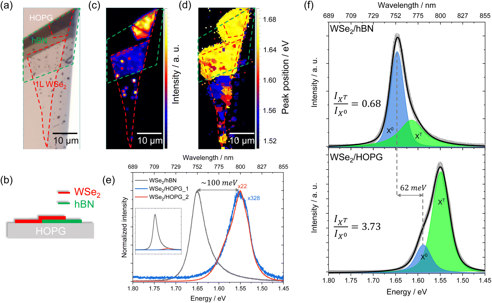 | ||
| Fig. 1 (a) Optical microscopy image and (b) schematic cross-section of the WSe2/hBN/HOPG hetero-stack. PL (c) intensity and (d) peak position map of the sample. (e) PL spectra of WSe2/hBN and WSe2/HOPG. For comparison, the PL intensity of WSe2/HOPG is normalized to that of WSe2/hBN. Inset: as-measured (not-normalized) PL spectra. (f) Fitted PL spectra of WSe2/hBN and WSe2/HOPG. | ||
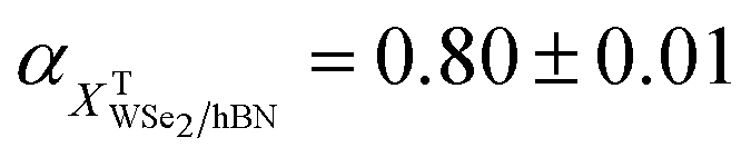
The detailed spectra of WSe2/hBN and WSe2/HOPG are shown in Fig. 1(e). A strong PL quenching of 1–2 orders of magnitude is observed when WSe2 is in contact with HOPG, which indicates charge dissociation through the junction or charge transfer between WSe2 and HOPG.34,35 Monolayer WSe2 on hBN shows a characteristic PL at ∼1.65 eV, which is consistent with the literature values,26,41 while the PL peak position of WSe2/HOPG shows a marked ∼100 meV redshift, which is much higher than the reported value caused by changing of the dielectric environment.18 Besides the quenching and redshift, the PL line shape changes significantly. We thus deconvoluted the PL spectra into peaks corresponding to the radiative recombination of different exciton/trion species in monolayer WSe2 (detailed fitting parameters can be found in the ESI†). As shown in Fig. 1(f), two peaks with a Voigt line shape were identified in the fitted spectra. The neutral exciton (X0) originates from the direct bandgap transition at the K point in the Brillouin zone and there is a charged exciton peak also known as trion XT.41–44 We also investigated the Stokes shift of monolayer WSe2 as shown in Fig. 3S,† which is negligible with a value of ∼2 meV. It is therefore fair enough to consider the PL peak position as the exciton energy. The fitting result suggests a 62 meV redshift of X0 and most interestingly, a drastic increase of the relative XT intensity. The ratio of IXT/IX0 increases from 0.68 ± 0.01 on hBN to 3.73 ± 0.04 on HOPG, which is strong evidence of a higher electron concentration in WSe2 on HOPG than in WSe2 on hBN.
Even though we propose that charge transfer and electron doping from HOPG to monolayer WSe2 seem to be the most reasonable mechanism of PL quenching, redshift, and increasing intensity ratio of trions to neutral excitons, we still carefully examined whether they originate from the defect-bound localized states or strain due to lattice mismatch. Power dependent PL intensities of WSe2/hBN and WSe2/HOPG are displayed in Fig. 2(a). The PL intensity is obtained from the integrated area of the Voigt fitted X0 and XT features. The PL intensity as a function of excitation laser power is then fitted by a power law: I ∝ Pα,41,45 where the extracted exponential factor  ,
,  ,
,  , and
, and 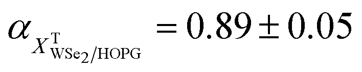 for X0 and XT on WSe2/hBN and WSe2/HOPG, respectively. The fitting results suggest a sublinear power dependence of the PL intensity for both X0 and XT on WSe2/hBN and WSe2/HOPG and do not show any saturation phenomena at high laser power, which excludes the possibility of defects as the origin of the observed behavior.46Fig. 2(b) shows the high spectral resolution (∼0.8 cm−1) Raman spectra of WSe2/hBN and WSe2/HOPG (only two spectra are shown in the main text for clarity, more spectra can be found in the ESI†). The most intense peak at ∼250 cm−1 corresponds to the combination of the in-plane E2g and out-of-plane A1g vibrational modes, which are almost degenerate at the same frequency.26,47–49 The feature at ∼260 cm−1 is a second order peak caused by a double resonance effect involving the longitudinal acoustic phonon at the M point in the Brillouin zone assigned as 2LA(M).49,50 The E2g/A1g mode is highly sensitive to the strain.51,52 The fitted Raman spectra reveal a small 0.15 cm−1 peak position difference, which indicates that strain is also small and cannot account for the huge redshift in PL.
 | ||
| Fig. 2 (a) PL intensity as a function of excitation power for X0 and XT emissions from WSe2/hBN and WSe2/HOPG. Solid lines are fits to a power law: I ∝ Pα. (b) High spectral resolution Raman spectra of WSe2/hBN and WSe2/HOPG. Inset is a zoom in at 248–252 cm−1. | ||
KPFM is a powerful technique to obtain the local surface potential and Fermi level position in the nanoscale.34,53 We therefore measured KPFM on the WSe2/hBN/HOPG hetero-stack to obtain further insight into the energy level alignment at the various interfaces. In the ideal case KPFM measures the contact potential difference (CPD) between the metallic AFM tip and the sample according to the relation: CPD = (ϕsample − ϕtip)/e, where ϕsample and ϕtip are the work functions of the sample and the tip, and e is the elementary charge. KPFM does not give a quantitative, absolute value of the Fermi level position under ambient conditions, because the CPD value is known to be strongly influenced by the measurement environment, tip geometry, and parasitic effects such as capacitive coupling, as well as the chosen experimental parameters.54–57 Nevertheless, it still qualitatively indicates the trend of the Fermi level position and material work functions.34,53,58,59 The values of the energy levels discussed in the following paragraph are directly extracted from the KPFM measurements.
Fig. 3(a) shows the CPD map of WSe2/hBN/HOPG. Even though it is the same monolayer WSe2 flake, one can clearly distinguish the high contrast between WSe2 on hBN and WSe2 on HOPG. The absolute work function of HOPG is determined to be ϕHOPG = 4.4 eV by the ultraviolet photoelectron spectroscopy (UPS) measurement shown in Fig. 10S.† The electron affinity of monolayer WSe2 is reported to be 3.7–3.9 eV.60,61 We therefore calculate and draw the band diagrams of WSe2 before (on hBN) and after (on HOPG) coming into contact with HOPG as shown in Fig. 3(b) and (c), respectively. The band diagrams reveal a decrease of the work function or increase of the Fermi level when WSe2 is in contact with HOPG, which indicates a higher electron concentration in WSe2 on HOPG than in WSe2 on hBN. The high electron concentration in WSe2/HOPG can only originate from electron doping from HOPG to WSe2, which explains the PL quenching, redshift, and increasing intensity ratio of trions to neutral excitons shown in Fig. 1.
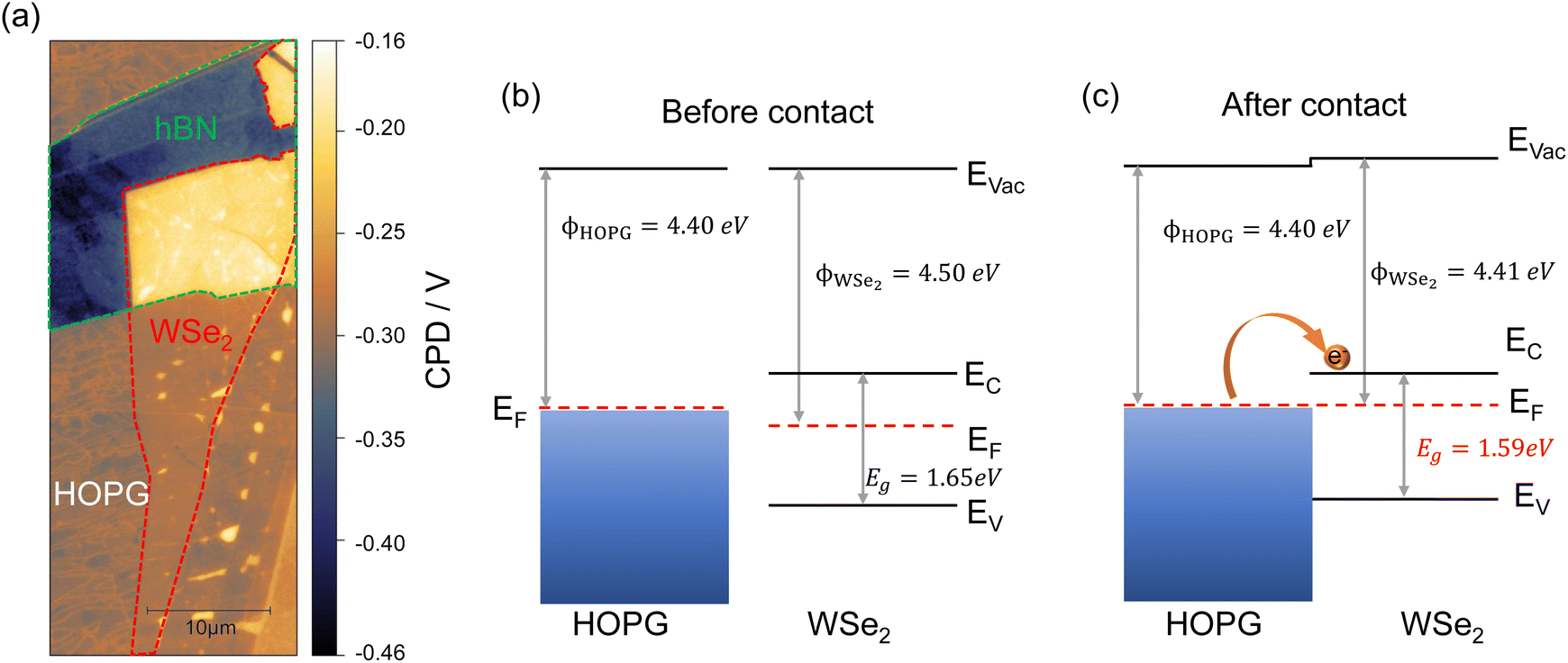 | ||
| Fig. 3 (a) KPFM of WSe2/hBN/HOPG. Band diagram of monolayer WSe2 and HOPG before (b) and after (c) contact. Before contact means when WSe2 is isolated from HOPG by hBN and after contact means that WSe2 is on HOPG. | ||
Apparently interfacing WSe2 with HOPG results in efficient tuning of the exciton emission in a straightforward manner. Researchers also studied the combination of WSe2 and graphene,18 yet did not report similar results. This naturally leads to the question: do graphene and graphite lead to a different interaction when interfaced with WSe2? To answer this question, we prepared a hetero-stack of WSe2/graphene/hBN/HOPG as shown in Fig. 4(a) and (b), where WSe2 is partially on hBN, partially on graphene, and partially on HOPG. The PL spectra of WSe2/hBN, WSe2/graphene, and WSe2/HOPG are shown in Fig. 4(c). Again, we observe a similar PL quenching, redshift, and increasing intensity ratio of trions to neutral excitons for WSe2 on HOPG. However, a redshift of only 20 meV is detected on WSe2/graphene, which is in excellent agreement with the value reported by Raja et al.18 This redshift of the A exciton is attributed to the altered local dielectric screening of the Coulomb interaction in WSe2. Besides the 20 meV redshift, there is a clear broadening of the PL for WSe2 on graphene compared with that of WSe2 on hBN. We consider that this broadening originates from the environmental dielectric disorder introduced by the several stamping steps during the sample preparation or the charge transfer between WSe2 and graphene.62,63 A higher trion emission intensity is also not observed in the case of WSe2/graphene. This clearly indicates that the interaction of WSe2 on graphene is different from that of WSe2 on HOPG. We assume that this difference is due to the lower amount of free electrons in graphene than that in HOPG. The KPFM measurement performed on such a sample is displayed in Fig. 4(d). A CPD contrast is only observed between WSe2/HOPG and WSe2/hBN with a value of ΔCPDWSe2/hBN−WSe2/HOPG = (20.4 ± 4.9) mV, while WSe2/graphene and WSe2/hBN reveal a negligible difference of ΔCPDWSe2/hBN−WSe2/gr = (2.4 ± 4.3) mV. This suggests that a significant change of the Fermi level position occurs due to electron doping from the substrate and only happens for WSe2 on HOPG but not for WSe2 on graphene. We use the mass action model to estimate the carrier concentration in the monolayers (details in the ESI†).64,65 Assuming that the radiative decay rates of excitons and trions are in the same order of magnitude as described in ref. 64, the electron concentration is in the range of ∼1013 cm−2 in monolayer WSe2 interfaced with HOPG, while it is approximately one magnitude smaller when interfaced with hBN or graphene.
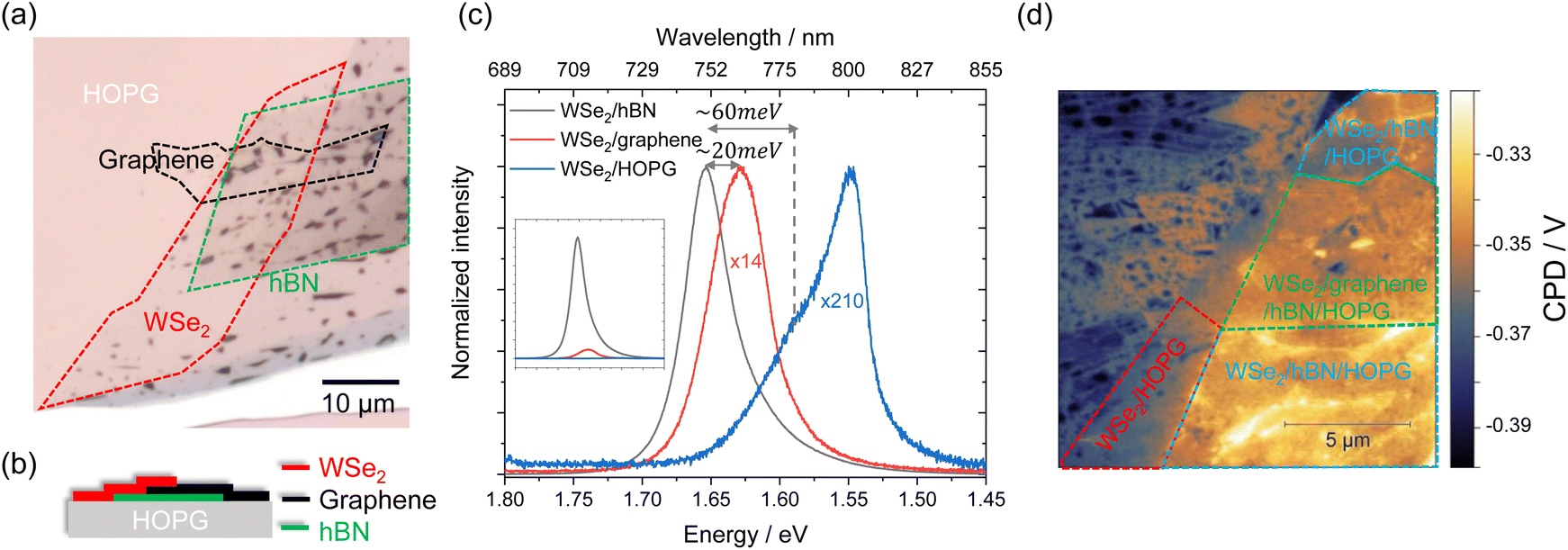 | ||
| Fig. 4 (a) Optical microscopy image and (b) schematic cross-section of the WSe2/graphene/hBN/HOPG hetero-stack. (c) PL spectra of WSe2/hBN, WSe2/graphene, and WSe2/HOPG. For comparison, the intensities of the WSe2/graphene and WSe2/HOPG PL are normalized to that of WSe2/hBN/HOPG. Inset: as-measured (not-normalized) PL spectra. (d) KPFM of WSe2/graphene/hBN/HOPG. | ||
4 Conclusions
In summary, we investigated WSe2/hBN, WSe2/graphene, and WSe2/HOPG hetero-stacks. We observed a strong PL intensity quenching, 62 meV redshift of the A exciton, and a drastic increase of the intensity ratio of trions to neutral excitons on WSe2/HOPG compared to WSe2/graphene and WSe2/hBN. The KPFM results reveal a high CPD contrast, which indicates a renormalization of the energy level alignment at the interface. The effects observed for WSe2 on HOPG are thus assigned to significant electron doping of the WSe2 monolayer from the HOPG substrate. We propose a simple yet efficient way to tune the exciton emission in monolayer WSe2 by substrate induced electron doping.Author contributions
Y. P. fabricated the samples, performed the measurements and analyzed the data. M. R., I. M. L. H., and T. I. M. contributed to data analysis and discussion. G. M., T. B. and A. W. performed the reflectance contrast measurement. M. A. A. and A. M. provided the graphene. D. R. T. Z. supervised the work. M. R. and D. R. T. Z. were involved in the evaluation and interpretation of the results. Y. P. wrote the manuscript. All authors discussed the results and commented on the manuscript.Conflicts of interest
The authors declare no conflict of interest.Acknowledgements
The authors gratefully acknowledge financial support by the Deutsche Forschungsgemeinschaft (DFG, projects ZA 146/43-1 and ZA 146/47-1). M. A. A. and A. M. acknowledge financial support by the Austrian Science Fund (FWF) under the grant no. I4323-N36. We thank Manuel Monecke for helping with the UPS measurement.References
- K. S. Novoselov, et al., Electric field effect in atomically thin carbon films, Science, 2004, 306, 666–669 CrossRef CAS.
- J. A. Wilson and A. Yoffe, The transition metal dichalcogenides discussion and interpretation of the observed optical, electrical and structural properties, Adv. Phys., 1969, 18, 193–335 CrossRef CAS.
- S. Wu, et al., Vapor–solid growth of high optical quality MoS2 monolayers with near-unity valley polarization, ACS Nano, 2013, 7, 2768–2772 CrossRef CAS PubMed.
- N. Peimyoo, et al., Thermal conductivity determination of suspended mono-and bilayer WS2 by Raman spectroscopy, Nano Res., 2015, 8, 1210–1221 CrossRef CAS.
- Y. Li, et al., Enhancement of exciton emission from multilayer MoS2 at high temperatures: intervalley transfer versus interlayer decoupling, Small, 2017, 13, 1700157 CrossRef.
- A. Splendiani, et al., Emerging photoluminescence in monolayer MoS2, Nano Lett., 2010, 10, 1271–1275 CrossRef.
- Y. Li, et al., Accurate identification of layer number for few-layer WS2 and WSe2 via spectroscopic study, Nanotechnology, 2018, 29, 124001 CrossRef.
- H. Tian, et al., Optoelectronic devices based on two-dimensional transition metal dichalcogenides, Nano Res., 2016, 9, 1543–1560 CrossRef.
- Z. Cheng, et al., 2D Materials Enabled Next-Generation Integrated Optoelectronics: from Fabrication to Applications, Adv. Sci., 2021, 8, 2003834 CrossRef.
- C. Zhou, et al., Self-driven WSe2 photodetectors enabled with asymmetrical van der Waals contact interfaces, NPJ 2D Mater. Appl., 2020, 4, 1–9 CrossRef.
- L. Lackner, et al., Tunable exciton-polaritons emerging from WS2 monolayer excitons in a photonic lattice at room temperature, Nat. Commun., 2021, 12, 1–6 CrossRef PubMed.
- S. Dufferwiel, et al., Exciton–polaritons in van der Waals heterostructures embedded in tunable microcavities, Nat. Commun., 2015, 6, 1–7 Search PubMed.
- T. Lin, et al., Many-body effects in doped WS2 monolayer quantum disks at room temperature, NPJ 2D Mater. Appl., 2019, 3, 1–6 CrossRef CAS.
- J. Xiao, et al., Nonlinear optical selection rule based on valley-exciton locking in monolayer WS2, Light Sci. Appl., 2015, 4, e366 CrossRef CAS.
- P. Gong, H. Yu, Y. Wang and W. Yao, Optical selection rules for excitonic Rydberg series in the massive Dirac cones of hexagonal two-dimensional materials, Phys. Rev. B, 2017, 95, 125420 CrossRef.
- B. M. Francis, et al., Two-dimensional Material based Printed Photonics: A Review, 2D Mater., 2022, 9(4), 042003 CrossRef.
- T. Tan, X. Jiang, C. Wang, B. Yao and H. Zhang, 2D material optoelectronics for information functional device applications: status and challenges, Adv. Sci., 2020, 7, 2000058 CrossRef CAS PubMed.
- A. Raja, et al., Coulomb engineering of the bandgap and excitons in two-dimensional materials, Nat. Commun., 2017, 8, 1–7 CrossRef.
- Y. Gong, et al., Band gap engineering and layer-by-layer mapping of selenium-doped molybdenum disulfide, Nano Lett., 2014, 14, 442–449 CrossRef CAS PubMed.
- H. J. Conley, et al., Bandgap engineering of strained monolayer and bilayer MoS2, Nano Lett., 2013, 13, 3626–3630 CrossRef CAS.
- R. Frisenda, et al., Biaxial strain tuning of the optical properties of single-layer transition metal dichalcogenides, NPJ 2D Mater. Appl., 2017, 1, 1–7 CrossRef.
- Z. Li, et al., Active light control of the MoS2 monolayer exciton binding energy, ACS Nano, 2015, 9, 10158–10164 CrossRef PubMed.
- P. V. Nguyen, et al., Visualizing electrostatic gating effects in two-dimensional heterostructures, Nature, 2019, 572, 220–223 CrossRef.
- L. Fernández, et al., Renormalization of the band gap in 2D materials through the competition between electromagnetic and four-fermion interactions in large N expansion, Phys. Rev. D, 2020, 102, 016020 CrossRef.
- A. Chaves, et al., Bandgap engineering of two-dimensional semiconductor materials, NPJ 2D Mater. Appl., 2020, 4, 1–21 CrossRef.
- P. Tonndorf, et al., Photoluminescence emission and Raman response of monolayer MoS2, MoSe2, and WSe2, Opt. Exp., 2013, 21, 4908–4916 CrossRef CAS.
- J. Xiao, M. Zhao, Y. Wang and X. Zhang, Excitons in atomically thin 2D semiconductors and their applications, Nanophotonics, 2017, 6, 1309–1328 CAS.
- W. Liu, et al., Strong exciton–plasmon coupling in MoS2 coupled with plasmonic lattice, Nano Lett., 2016, 16, 1262–1269 CrossRef CAS.
- J. S. Ross, et al., Electrically tunable excitonic light-emitting diodes based on monolayer WSe2 p–n junctions, Nat. Nanotechnol., 2014, 9, 268–272 CrossRef CAS.
- M. Ferrera, et al., Controlling excitons in the quantum tunneling regime in a hybrid plasmonic/2D semiconductor interface, Appl. Phys. Rev., 2022, 9, 031401 CAS.
- A. Castellanos-Gomez, et al., Deterministic transfer of two-dimensional materials by all-dry viscoelastic stamping, 2D Mater., 2014, 1, 011002 CrossRef CAS.
- Y. Pan, S. Li, M. Rahaman, I. Milekhin and D. R. T. Zahn, Signature of lattice dynamics in twisted 2D homo/hetero-bilayers, 2D Mater., 2022, 9, 045018 CrossRef.
- L. Ding, et al., Understanding interlayer coupling in TMD-HBN heterostructure by Raman spectroscopy, IEEE Trans. Electron Devices, 2018, 65, 4059–4067 Search PubMed.
- R. R. Rojas-Lopez, et al., Photoluminescence and charge transfer in the prototypical 2D/3D semiconductor heterostructure MoS2/GaAs, Appl. Phys. Lett., 2021, 119, 233101 CrossRef.
- Y. Hwang, T. Kim and N. Shin, Interlayer Energy Transfer and Photoluminescence Quenching in MoSe2/Graphene van der Waals Heterostructures for Optoelectronic Devices, ACS Appl. Nano Mater., 2021, 4, 12034–12042 CrossRef.
- B. Zheng, et al., WO3–WS2 vertical bilayer heterostructures with high photoluminescence quantum yield, J. Am. Chem. Soc., 2019, 141, 11754–11758 CrossRef CAS PubMed.
- W. Zheng, et al., Defect-induced distinct exciton-exciton interactions in WS2 monolayers, Sci. China Mater., 2022, 1–9, 2502–2510 CrossRef.
- D. Purdie, et al., Cleaning interfaces in layered materials heterostructures, Nat. Commun., 2018, 9, 1–12 CrossRef.
- S. J. Haigh, et al., Cross-sectional imaging of individual layers and buried interfaces of graphene-based heterostructures and superlattices, Nat. Mater., 2012, 11, 764–767 CrossRef CAS.
- A. V. Tyurnina, et al., Strained bubbles in van der Waals heterostructures as local emitters of photoluminescence with adjustable wavelength, ACS Photonics, 2019, 6, 516–524 CrossRef CAS.
- J. Huang, T. B. Hoang and M. H. Mikkelsen, Probing the origin of excitonic states in monolayer WSe2, Sci. Rep., 2016, 6, 1–7 CrossRef PubMed.
- E. Liu, et al., Valley-selective chiral phonon replicas of dark excitons and trions in monolayer WSe2, Phys. Rev. Res., 2019, 1, 032007 CrossRef CAS.
- M. He, et al., Valley phonons and exciton complexes in a monolayer semiconductor, Nat. Commun., 2020, 11, 1–7 CrossRef.
- Z. Li, T. Wang, S. Miao, Z. Lian and S.-F. Shi, Fine structures of valley-polarized excitonic states in monolayer transitional metal dichalcogenides, Nanophotonics, 2020, 9, 1811–1829 CrossRef.
- Z. Wu, et al., Defects as a factor limiting carrier mobility in WSe2: a spectroscopic investigation, Nano Res., 2016, 9, 3622–3631 CrossRef.
- Z. Wu and Z. Ni, Spectroscopic investigation of defects in two-dimensional materials, Nanophotonics, 2017, 6, 1219–1237 Search PubMed.
- X. Luo, et al., Effects of lower symmetry and dimensionality on Raman spectra in two-dimensional WSe2, Phys. Rev. B, 2013, 88, 195313 CrossRef.
- W. Zhao, et al., Lattice dynamics in mono-and few-layer sheets of WS2 and WSe2, Nanoscale, 2013, 5, 9677–9683 RSC.
- H. Terrones, et al., New first order Raman-active modes in few layered transition metal dichalcogenides, Sci. Rep., 2014, 4, 1–9 Search PubMed.
- E. Del Corro, et al., Excited excitonic states in 1L, 2L, 3L, and bulk WSe2 observed by resonant Raman spectroscopy, ACS Nano, 2014, 8, 9629–9635 CrossRef CAS.
- A. Dadgar, et al., Strain engineering and Raman spectroscopy of monolayer transition metal dichalcogenides, Chem. Mater., 2018, 30, 5148–5155 CrossRef CAS.
- S. B. Desai, et al., Strain-induced indirect to direct bandgap transition in multilayer WSe2, Nano Lett., 2014, 14, 4592–4597 CrossRef CAS.
- W. Melitz, J. Shen, A. C. Kummel and S. Lee, Kelvin probe force microscopy and its application, Surf. Sci. Rep., 2011, 66, 1–27 CrossRef CAS.
- C. E. Giusca, et al., Water affinity to epitaxial graphene: the impact of layer thickness, Adv. Mater. Interfac., 2015, 2, 1500252 CrossRef.
- H. Jacobs, P. Leuchtmann, O. Homan and A. Stemmer, Resolution and contrast in Kelvin probe force microscopy, J. Appl. Phys., 1998, 84, 1168–1173 CrossRef CAS.
- S. Barbet, et al., Cross-talk artefacts in Kelvin probe force microscopy imaging: a comprehensive study, J. Appl. Phys., 2014, 115, 144313 CrossRef.
- H. Jacobs, H. Knapp and A. Stemmer, Practical aspects of Kelvin probe force microscopy, Rev. Sci. Instrum., 1999, 70, 1756–1760 CrossRef CAS.
- E. G. Castanon, et al., Calibrated Kelvin-probe force microscopy of 2D materials using Pt-coated probes, J. Phys. Commun., 2020, 4, 095025 CrossRef CAS.
- A. Matkovia, et al., Interfacial band engineering of MoS2/gold interfaces using pyrimidine-containing self-assembled monolayers: toward contact-resistance-free bottom-contacts, Adv. Electron. Mater., 2020, 6, 2000110 CrossRef.
- J. Xiao, Y. Zhang, H. Chen, N. Xu and S. Deng, Enhanced performance of a monolayer MoS2/WSe2 heterojunction as a photoelectrochemical cathode, Nano-Micro Lett., 2018, 10, 1–9 CrossRef PubMed.
- W. Liu, W. Cao, J. Kang and K. Banerjee, High-performance field-effect-transistors on monolayer-WSe2, ECS Trans., 2013, 58, 281 CrossRef.
- A. Raja, et al., Dielectric disorder in two-dimensional materials, Nat. Nanotechnol., 2019, 14, 832–837 CrossRef CAS.
- X. Xing, et al., Tunable ultrafast electron transfer in WSe 2–graphene heterostructures enabled by atomic stacking order, Nanoscale, 2022, 14, 7418–7425 RSC.
- S. Mouri, Y. Miyauchi and K. Matsuda, Tunable photoluminescence of monolayer MoS2 via chemical doping, Nano Lett., 2013, 13, 5944–5948 CrossRef CAS.
- J. S. Ross, et al., Electrical control of neutral and charged excitons in a monolayer semiconductor, Nat. Commun., 2013, 4, 1–6 Search PubMed.
Footnote |
| † Electronic supplementary information (ESI) available. See DOI: https://doi.org/10.1039/d2na00495j |
| This journal is © The Royal Society of Chemistry 2022 |