
 Open Access Article
 This Open Access Article is licensed under a Creative Commons Attribution-Non Commercial 3.0 Unported Licence
Surface etching and edge control of hexagonal boron nitride assisted by triangular Sn nanoplates†
Hsin
Yi
a,
Pablo
Solís-Fernández
b,
Hiroki
Hibino
c and
Hiroki
Ago
 *ab
*ab
aInterdisciplinary Graduate School of Engineering Sciences, Kyushu University, Fukuoka 816-8580, Japan. E-mail: ago.hiroki.974@m.kyushu-u.ac.jp
bGlobal Innovation Center (GIC), Kyushu University, Fukuoka 816-8580, Japan
cSchool of Engineering, Kwansei Gakuin University, Hyogo 669-1330, Japan
First published on 8th August 2022
Abstract
Hexagonal boron nitride (hBN) is an ideal insulating substrate and template for other two-dimensional (2D) materials. The combination of hBN and 2D materials of group IV atoms, such as graphene, is interesting, because it can offer attractive physical properties and promising applications. Here, we demonstrate the unique behavior of tin (Sn), one of the group IV elements, on multilayer hBN which was grown by chemical vapor deposition (CVD). At high temperatures, triangular nanoplates formed after thermal deposition of Sn on the hBN surface, with their orientations determined by the hBN lattice. The triangular Sn nanoplates moved on the hBN surface, leaving monolayer-deep nanotrenches. Low-energy electron microscopy (LEEM) revealed that the nanotrenches are aligned in the armchair directions of the hBN. Furthermore, an additional Ar annealing without supplying Sn vapor induced the structural change of the linear trenches to triangular pits, indicating the preferential formation of zigzag edges in the absence of Sn. Our work highlights the unique behavior of Sn on hBN and offers a novel route to engineer the hBN surface.
Introduction
Hexagonal boron nitride (hBN), a two-dimensional (2D) insulator with a large band gap of 5.9 eV, is a promising material for a wide range of unique applications, such as tunnel magnetoresistance (TMR) devices, ultraviolet light emission diodes (LEDs), gas barrier films, templates for functional films, dielectrics for quantum circuits, and bright single-photon emitters.1–7 Due to its atomically flat surface and thermal/chemical stability, hBN is an ideal substrate and surface protective layer for other 2D materials. Hence, using multilayer hBN as a support and/or protection layer allows the observation of the intrinsic electronic, optical, and magnetic properties of graphene and transition metal dichalcogenides (TMDCs).8–10 The use of hBN has boosted emerging research in different 2D materials, such as superconducting and correlated states in twisted bilayer graphene (BLG) and moiré excitons in TMDC bilayers.11–13 These exciting physical phenomena can be observed when the 2D materials are protected by encapsulation within multilayer hBN.hBN is also a promising template for the growth/deposition of other functional materials, such as GaN, VO2, Fe3O4, and polythiophene.14–17 It can also work as a release layer to assist the transfer from the growth substrates to other substrates.18 Besides, 2D Sn with the √7 × √7 phase has been reported on hBN/Ir(111).19 Thus, the interaction between Sn metal and the hBN surface is interesting.
It has been reported that transition metals can interact with hBN at high temperatures in the presence of H2, leading to the formation of triangular holes.20,21 Besides, several reports have shown that transition metal nanoparticles can be used to create etched trenches on the hBN surface.22–25 Wang et al. demonstrated that Ni and Pt nanoparticles show different etching behaviors of hBN when heating in H2, with the etching following the zigzag and armchair directions of the hBN, respectively.24 It is interesting that the etching directions can be defined by the interaction between the metal species and the relatively complex structure of hBN, with its alternating network of B and N atoms. The nanotrenches made by the metal-assisted etching can be further applied to grow graphene nanoribbons (GNRs), with the edges controlled by the side edges of the hBN trenches.22,24 Therefore, nanoparticle-assisted etching offers a novel route to pattern hBN surfaces and fabricate nanomaterials with well-controlled edge structures.
Compared with graphene, hBN is more difficult to etch because of its high thermal and chemical stability.3,4 Several reports have shown the oxidative etching of hBN by heating in air.4,26 Some specific methods to etch hBN have also been developed, such as the use of high pressure CF4 plasma to selectively etch hBN from heterostacks with graphene.27 Alternating O2 and N2 plasma treatments was also shown to induce layer-by-layer etching of hBN.28 Besides, electron beam-induced etching of hBN has also been demonstrated.29 Compared to these methods, the nanoparticle-assisted etching approach has the advantage of allowing the creation of more elaborated patterns under milder conditions.
Here, we present the unique behavior of Sn on hBN surface at high temperatures. We found that thermally deposited Sn on the hBN surface forms triangular nanoplates. These nanoplates can move along the armchair directions of hBN, resulting in the formation of monolayer-deep nanotrenches on the hBN surface. The Sn-assisted etching is different from the previous literature of hBN etching with transition metal nanoparticles,22–25 because Sn does not require H2 gas to etch hBN. Furthermore, the nanotrenches will change their shape when they are further annealed in Ar without supplying Sn vapor, leading to energetically more favorable zigzag edge terminations. Our work highlights the unique behavior of liquid Sn on hBN surfaces and provides an interesting route to modify the surface morphology of multilayer hBN.
Experimental
Synthesis of multilayer hBN
Multilayer hBN was grown by low-pressure CVD at 1200 °C on a Fe–Ni alloy catalyst with borazine (B3N3H6) feedstock using a procedure adapted from our previous works.30,31 The as-grown multilayer hBN was transferred by spin-coating a polymethyl methacrylate (PMMA) film, and then chemically etching the Fe–Ni catalyst. After transferring the PMMA/hBN stack on a SiO2/Si substrate, the PMMA was removed by acetone. The hBN thickness measured by atomic force microscope (AFM) varied between 1 and 10 nm across the surface.Etching of hBN with Sn
Sn powder (70 mg) and a 1 cm2 hBN/SiO2 substrate were placed at the upstream and center of a quartz tube within a furnace, respectively, as shown in Fig. 1a. The temperature was increased to 850–1100 °C, depending on the experiment, under a flow of high-purity Ar gas (99.999%) at ambient pressure. After keeping the same temperature for 30 minutes, the furnace was cooled down naturally.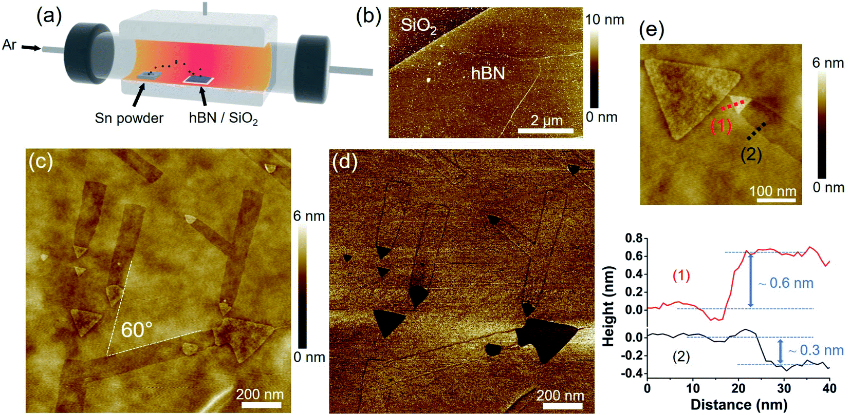 | ||
| Fig. 1 (a) Setup used to deposit Sn on multilayer hBN at high temperatures. (b) AFM image of a multilayer hBN on SiO2 before the annealing. AFM height (c) and phase (d) images of the hBN after annealing with Sn vapor at 1000 °C for 30 min. (e) AFM height image (upper panel) and the height profile of the corresponding nanoplate and nanotrench (lower panel). | ||
Sn-free annealing
After being etched with Sn and characterized, the sample was placed at the center of the quartz tube and annealed at 1000 °C for 10 minutes under an Ar flow at ambient pressure without placing Sn powder at the upstream. The furnace was cooled down naturally after the annealing.Characterizations
AFM images were taken with a Bruker Nanoscope V. Low-energy electron microscopy (LEEM) images and low-energy electron diffraction (LEED) patterns were measured with a Elmitec LEEM III. The scanning electron microscope (SEM) image was taken with a Hitachi S-4800. Energy-dispersive X-ray spectroscopy (EDS) was measured with a Bruker QUANTAX FlatQUAD.Results and discussion
Etching of hBN with triangular Sn nanoplates
Fig. 1b shows an AFM image of a multilayer hBN before the annealing with Sn vapor. The pristine hBN had a flat surface with the thickness of 1–10 nm across the surface. hBN with different thickness and a relatively large area (∼1 cm2) obtained by CVD allowed us to study the behavior of Sn on different thicknesses of hBN. hBN wrinkles, which formed due to the different thermal expansion coefficients of the Fe–Ni catalyst and hBN, were also observed on the hBN surface (see Fig. 1b).Fig. 1c shows an AFM image of the hBN after the annealing with Sn vapor at 1000 °C. Straight and shallow nanotrenches with widths ranging from 50 to 130 nm can be seen on the surface. Each nanotrench was terminated with an equilateral triangular nanoplate at the end, and the side length of each triangular nanoplate matched the width of the corresponding nanotrench. These observations indicate that the nanotrenches are the traces left by the movement of the triangular nanoplates while etching the hBN. As shown in Fig. 1c, all the triangular nanoplates have the same orientation. The nanotrenches are also oriented along three directions separated by 60° as indicated by the dashed lines. These results imply that the etching is related to the crystallographic orientation of the hBN. Fig. 1d is the AFM phase image corresponding to the same area as Fig. 1c. Under certain circumstances, the contrast of the AFM phase image can be interpreted as regions with different physical and chemical properties.32 The phase of the hBN surface and the nanotrenches were the same. However, the triangular nanoplates had a different phase, suggesting that they are not hBN and likely consist of Sn. The SEM-EDS analysis also confirmed the existence of Sn, as shown in Fig. S1.†
The AFM height profile in Fig. 1e indicates that the depth of the nanotrench is ∼0.3 nm, which roughly corresponds to the thickness of one hBN layer. The triangular nanoplate is higher than the hBN surface, with the height difference being less than 1 nm. During heating, Sn may start depositing on the hBN surface and form triangular nanoplates. When the temperature is high enough, the nanoplates can move on the hBN surface, leaving monolayer-deep nanotrenches.
It has been reported that Ni and Pt nanoparticles also make linear etched trenches on the hBN surface.22–25 However, our work has two main differences from the previous studies: (i) in our case the etching occurs with triangular nanoplates instead of spherical nanoparticles, (ii) H2 was not introduced during our process. Therefore, the interaction between Sn and hBN, and the etching mechanism should be different from that reported for transition metal nanoparticles.
Characterizations of etched trenches on hBN surface
To determine the lattice orientation of the nanotrenches, low-energy electron microscopy (LEEM) measurements were performed. To avoid charging during the LEEM observation, single-layer graphene (SLG) was transferred on top of the hBN/SiO2. Fig. 2a is a bright-field LEEM (BF-LEEM) image with some nanotrenches highlighted in red and the corresponding nanoplates highlighted in yellow. The low-energy electron diffraction (LEED) pattern obtained from the green circle is shown in Fig. 2b. The six bright diffraction spots in the LEED pattern were from the SLG on the top. Three faint spots highlighted by green circles can be assigned to the diffraction from the hBN, which has a three-fold symmetry. The diffraction spots from the hBN were much weaker than those of the SLG since the incident and scattered electrons were attenuated by the SLG. From the relative orientation of the nanotrenches (Fig. 2a) and the orientation of reciprocal lattice of the hBN (Fig. 2b), we can conclude that the nanotrenches are aligned along the armchair directions of hBN. Fig. 2c shows the two possible orientations of the triangular nanoplates relative to the top hBN layer. Since the orientation of the hBN can be determined by the LEED pattern,33–35 comparison of the triangular nanoplates and the LEED pattern (see Fig. 2a and b) confirmed that the nanoplates have the orientation Sn(1), whose edges are parallel to the N-terminated zigzag directions of the hBN. This indicates that the atomic arrangement of B and N atoms strongly affects the formation and orientation of the triangular nanoplates. Orientations of the triangular nanoplates and the nanotrenches are summarized in Fig. 2d.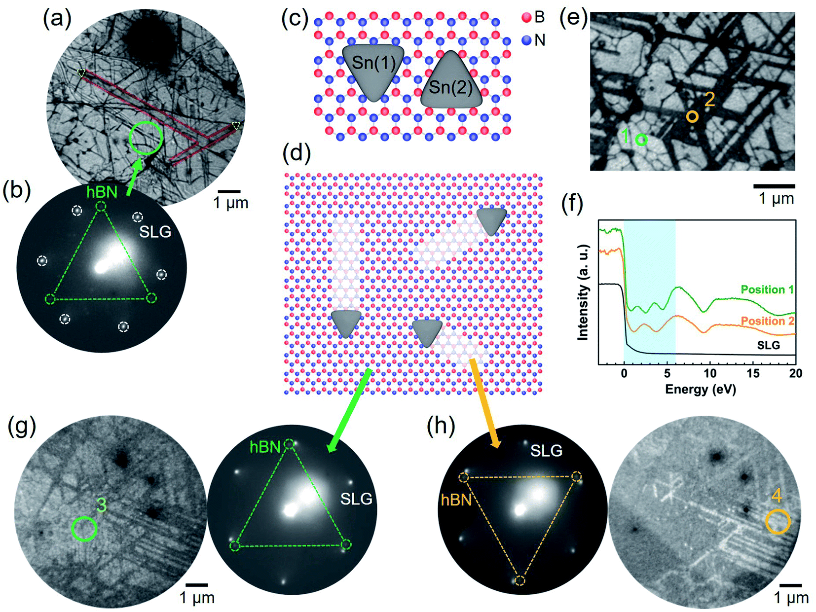 | ||
| Fig. 2 (a and b) BF-LEEM image of nanotrenches and the LEED pattern measured at the marked position. LEEM and LEED were measured with electron energies of 6 eV and 35 eV, respectively. (c) Possible orientations of the triangular nanoplates relative to the hBN lattice. (d) Schematic of the hBN surface with triangular nanoplates moving in armchair directions. (e) BF-LEEM image of the etched trenches measured with an electron energy of 3.8 eV. (f) LEER spectra measured at the marked positions in (e). For comparison the spectrum of SLG is also depicted. (g and h) DF-LEEM images measured with an electron energy of 36 eV using (10) and (01) diffraction spots, respectively. The LEED patterns were measured at the marked positions (3 and 4). | ||
The single-atom depth of the nanotrenches can also be determined by LEEM. Fig. 2e and f show the BF-LEEM image and the low-energy electron reflectivity (LEER) spectra, respectively, of an area which was extensively etched. For comparison, the LEER spectrum of a single-layer graphene was also included in Fig. 2f. Previous studies have reported that the interlayer states of hBN cause oscillations of the reflectivity in the low energy region. The number of minima in the LEER spectrum relates to the number of layers, with the appearance of n reflectivity minima representing the existence of n + 1 layers.34,35 This is valid for hBN as well as graphene.35 The spectra shown in Fig. 2f were collected at a flat non-etched area (position 1) and within nanotrenches (position 2). At position 1, three reflectivity minima can be observed in the 0–6 eV range (blue background in Fig. 2f), representing the existence of four layers (3L-hBN and 1L-graphene). At the position 2, two reflectivity minima can be observed, representing the existence of three layers (2L-hBN and 1L-graphene). Therefore, the LEER spectra also prove that the nanotrenches have single-atom depth, which is consistent with the AFM height profile (Fig. 1e).
Assuming that the multilayer hBN has AA′ stacking, this top layer etching can also be observed by the LEED measurement. Fig. 2g and h compare the dark-field LEEM (DF-LEEM) images of the same area using the (10) and (01) diffraction spots of the hBN, respectively. Reflecting the AA′ stacking, the non-etched and etched areas have opposite contrasts in the dark field images, making the nanotrenches clear in the images. Diffraction patterns collected from the marked positions (3 and 4) revealed that there is a 60° rotation of the top hBN layer relative to the hBN layer of the nanotrenches. These DF-LEEM images provide additional evidence that the etching occurred only at the top hBN layer, exposing the second layer of hBN at the nanotrenches.
Effects of annealing temperature and hBN thickness
Fig. 3 compares the AFM images of thin (1–2 nm) and thick (>4 nm) hBN after the annealing with Sn vapor at three different temperatures (850, 1000, and 1100 °C). At the thin hBN areas, many triangular nanoplates with the same orientation were observed after the annealing at 850 °C (Fig. 3a). However, no nanotrenches were created on the hBN surface at this low temperature. When the annealing temperature was increased to 1000 °C, nanotrenches could be observed on the hBN surface, indicating that the nanoplates were thermally activated and they were moving on the hBN surface (Fig. 3b). The annealing at 1100 °C produced wider nanotrenches than those produced at 1000 °C. Besides, when annealing at 1100 °C a number of spherical nanoparticles were attached to the edges of the nanotrenches (Fig. 3c). We speculate that at the high temperatures, some Sn nanoparticles may be left at the edges while the Sn nanoplate was etching the hBN. This behavior explains the observed gradual decrease of the width of the nanotrenches as the nanoplate was losing Sn (see Fig. 3c).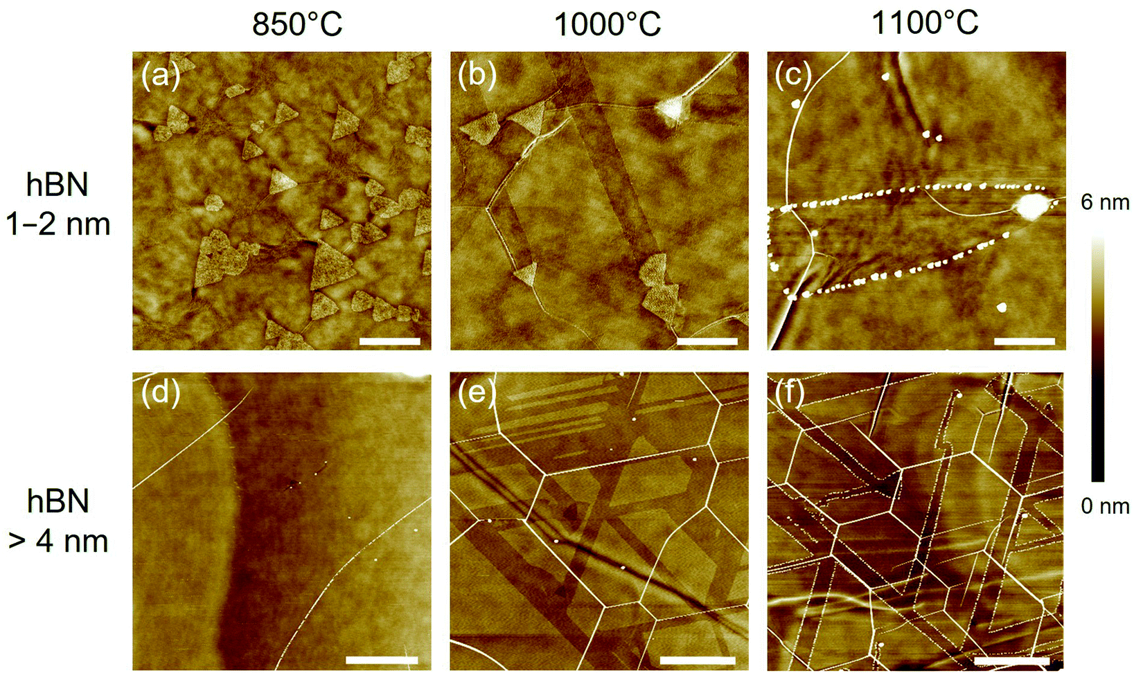 | ||
| Fig. 3 Comparison of the thin and thick hBN areas after the annealing with Sn vapor at 850 °C, 1000 °C and 1100 °C for 30 min. (a–c) AFM images of the thin hBN areas (1–2 nm). The scale bars are 200 nm. (d–f) AFM images of the thick hBN areas (>4 nm). The scale bars are 1 μm. | ||
In the case of thick hBN (>4 nm), no etched trenches nor nanoplates were observed after the annealing at 850 °C (Fig. 3d). Increasing the annealing temperature to 1000 °C produced etched trenches on the hBN surface. Sn nanoplates can create long etched trenches on the flat surface of thick hBN. The trenches connect with each other, and some areas are extensively etched (Fig. 3e). The sample at 1100 °C shows well-oriented etched trenches (Fig. 3f). As seen in Fig. 3f, a spherical nanoparticle is located at the end of some of the etched trenches. Although the etching may also start with the triangular Sn nanoplates, the gradual loss of Sn to the edges of the trenches results in the decrease of both the size of the original nanoplates and the width of the etched trenches. Eventually, only Sn nanoparticles can be observed on the surface. The loss of Sn to the edges observed at 1100 °C may also occur at 1000 °C but with a lower rate.
On the other hand, we speculate that triangular nanoplates observed at the thin hBN areas are initially composed of metallic Sn during the hBN etching process. Because hBN is very thin, after the etching Sn can go down and reach the SiO2 surface, forming a Sn–SiO2 alloy. Once the alloying occurs, the triangular nanoplate would “freeze” and stay at the same position.
It is noted that many hBN wrinkles can be observed after the annealing at the high temperatures (1000 and 1100 °C, see Fig. 3e and f). The hBN wrinkles, which have been previously described for the case of Al2O3 substrate,36 are thought to arise from the different thermal expansion coefficients of the hBN and the SiO2 substrate. In particular, the 1100 °C sample showed high-density and well-oriented wrinkles. It was reported that hBN wrinkles tend to form along armchair directions due to the anisotropic 2D structure.36 As seen in Fig. 3e and f, the etched trenches are parallel to the hBN wrinkles, being an additional evidence of the hBN etching in armchair directions.
Edge structure change induced by Sn-free annealing
It is noted that no nanotrenches appeared after annealing the pristine hBN at 1000 °C under an Ar flow without Sn powder at the upstream (Fig. S2†), indicating that the etching observed so far is due to the presence of Sn. However, we found that the edges of the etched trenches are active upon further annealing under the same conditions (1000 °C, Ar flow) but without supplying Sn vapor. This allowed an additional change of the nanotrench edge structures. Fig. 4a shows the AFM image of three nanotrenches before the additional Sn-free annealing. After a 10 min Sn-free annealing, the nanotrenches became wider, which can be seen in Fig. 4b. Besides, the nanotrenches still retained a single-atom depth during the edge structure change. Compared to the flat hBN surface, the nanotrench edges are more active due to the presence of dangling bonds and vacancies; therefore, the etching proceeded selectively. It is noted that in some cases, the hBN near the triangular nanoplates was damaged after Sn-free annealing, which was probably because the Sn inside the nanoplates melted and diffused during the heat treatment, as shown in Fig. S3.†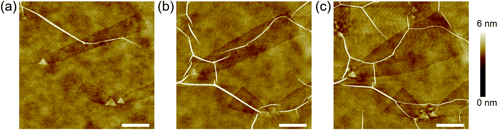 | ||
| Fig. 4 Evolution of the edge structure of nanotrenches induced by Sn-free annealing. AFM images measured before (a) and after annealing in Ar without supplying Sn vapor at 1000 °C for 10 min (b) and 20 min (c). The scale bars are 200 nm. | ||
Additional 10 min Sn-free annealing further changed the shape of the nanotrenches, resulting in near triangular pits (Fig. 4c). As discussed in Fig. 2c (Sn(1)), the triangular nanoplates have the edges parallel to the N-terminated zigzag directions. Fig. 4c shows that the width of the etched patterns increases as the distance from the nanoplates increases. Therefore, the armchair edges will change to the N-terminated zigzag edges instead of B-terminated zigzag edges during the Sn-free annealing, as compared in Fig. S4.† Our observations are in agreement with the theoretical calculation proposing that N-terminated zigzag edges are more stable than armchair and B-terminated zigzag edges.37 It is noted that after each annealing step, the morphology of the hBN wrinkles changed and their density increased due to the additional strain induced by the heat treatment (see Fig. 4a–c).
Mechanism of triangular nanoplate formation and subsequent etching
Fig. 5a–d illustrate the proposed model of the linear etching of hBN with a triangular Sn nanoplate. After the deposition of Sn from the vapor phase, Sn might form a triangular nanoplate whose orientation is determined by the underlying hBN lattice due to their interaction and the anisotropic hBN atomic arrangement (Fig. 5a and b). At sufficiently high temperatures (1000 °C or higher), the nanoplate can move along one of the armchair directions of hBN, resulting in a monolayer-deep nanotrench on the hBN surface (Fig. 5c and d). A little amount of Sn might be left at the edges during etching, resulting in the gradual decrease of the size of the Sn nanoplate.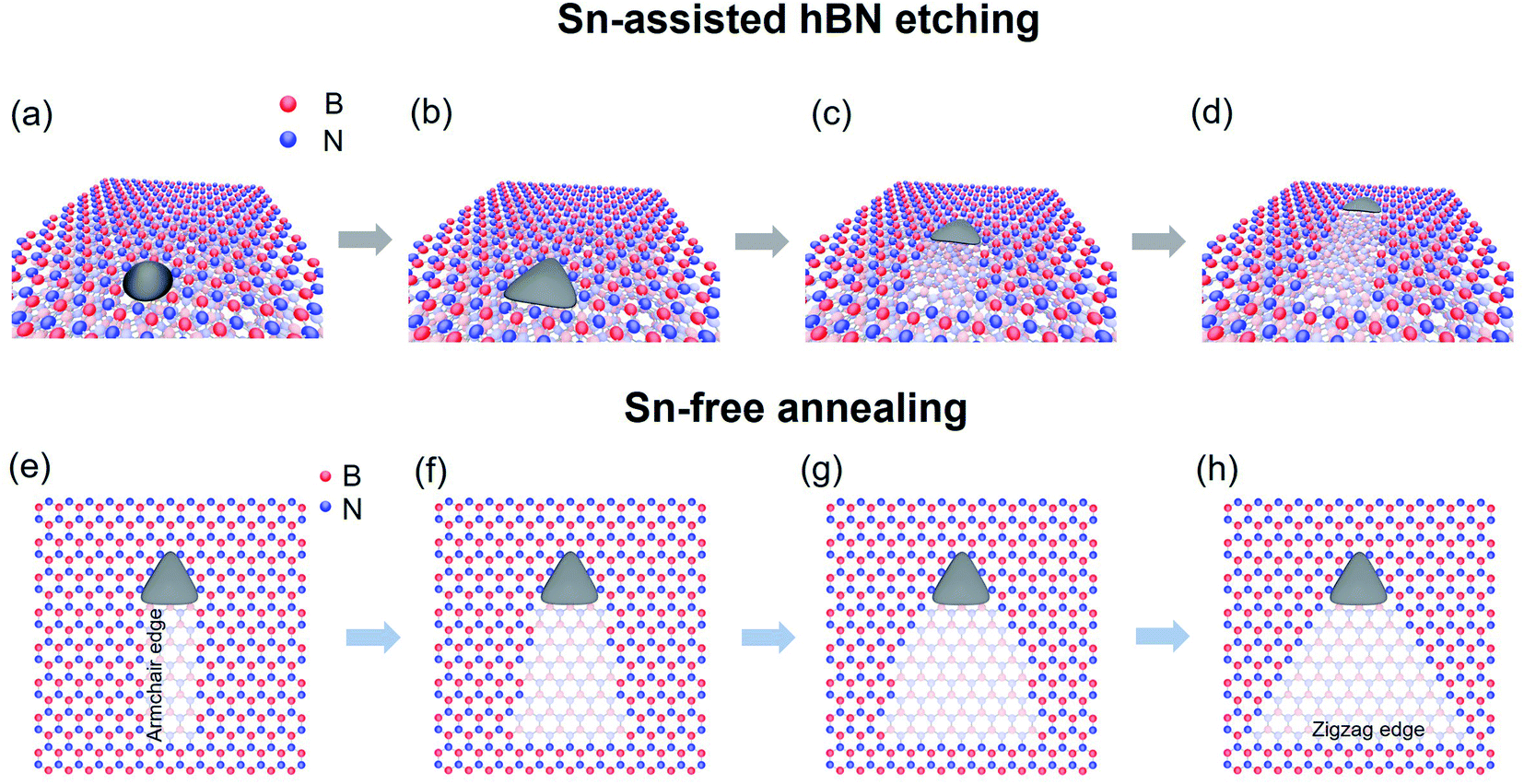 | ||
| Fig. 5 Schematic of the linear etching of top layer hBN with a triangular nanoplate (a–d), and the further edge structure change induced by Sn-free annealing (e–h). | ||
If the nanotrench is further annealed without supplying Sn vapor, the nanotrench with armchair edges will experience structural changes. Reflecting the lower stability of the armchair edges, the nanotrench will become a triangular pit with N-terminated zigzag edges in the end (Fig. 5e–h). The edge-controlled etching in this work can be understood as follows. It has been reported that depending on the nanoparticle catalysts, etching of hBN can occur in different etching directions (zigzag or armchair).24,25 In this work, hBN etching with Sn proceeds along the armchair directions. During the Sn-free annealing, the armchair edges are energetically less favorable at the high temperatures. Therefore, if the etching is not driven by Sn, there is a tendency to form N-terminated zigzag edges.
As the Sn-assisted etching can be carried out in a hydrogen-free environment, the mechanism of Sn-assisted etching can be largely different from the Pt and Ni nanoparticle-assisted etching using H2 gas.22–25 Although our experiments were conducted under the flow of high-purity Ar gas (99.999%), we cannot rule out the presence of a trace amount of oxygen, which may be due to the impurities in Ar or released from the quartz tube and other elements of the experimental setup. However, we consider that the etching is mainly driven by Sn. First, no nanotrenches appeared after annealing at 1000 °C in the absence of Sn (see Fig. S2†). Second, the oxidative etching of hBN in the previous reports is less anisotropic compared to the etching observed in the case of Sn.4,26
As far as we know, this is the first report demonstrating etching of a 2D material by triangular nanoplates. Further studies are needed to understand the detailed formation mechanism of the unique triangular nanoplates and the Sn-assisted hBN etching mechanism.
Conclusions
We have demonstrated the formation of unique triangular Sn nanoplates and the subsequent etching of hBN with these nanoplates. We found that the triangular nanoplates move on the hBN surface along armchair directions, resulting in the formation of monolayer-deep nanotrenches. This method has the advantages that it can be carried out in one step and does not require hydrogen gas. Moreover, Sn-free annealing induced the edge structure change of the nanotrenches from armchair edges to zigzag edges, leading to the formation of triangular pits on the hBN surface. This work not only offers the interesting behavior of Sn on hBN but also provides a facile approach to pattern hBN surfaces, expanding the potential of hBN for 2D device integration.Author contributions
H. A., P. S.-F., H. Y. designed the experiments. H. Y. prepared samples and performed most of the measurements. H. H. performed LEEM/LEED measurements and analysis. H. Y., H. A., P. S.-F. wrote the manuscript. All authors discussed the data and results.Conflicts of interest
There are no conflicts to declare.Acknowledgements
This work was supported by the JSPS Grant-in-Aid for Scientific Research on Innovative Areas “Science of 2.5 Dimensional Materials: Paradigm Shift of Materials Science Toward Future Social Innovation” (KAKENHI grant numbers JP21H05232, JP21H05233), and JSPS KAKENHI grant numbers JP21K18878, JP21H01768, JP20H05670, JP18H03864, JST CREST grant numbers JPMJCR18I1, JPMJCR20B1, and the JSPS A3 Foresight Program.Notes and references
- Z. Wang, D. Sapkota, T. Taniguchi, K. Watanabe, D. Mandrus and A. F. Morpurgo, Nano Lett., 2018, 18, 4303–4308 CrossRef CAS PubMed.
- D. A. Laleyan, S. Zhao, S. Y. Woo, H. N. Tran, H. B. Le, T. Szkopek, H. Guo, G. A. Botton and Z. Mi, Nano Lett., 2017, 17, 3738–3743 CrossRef CAS PubMed.
- Z. Liu, Y. Gong, W. Zhou, L. Ma, J. Yu, J. C. Idrobo, J. Jung, A. H. MacDonald, R. Vajtai, J. Lou and P. M. Ajayan, Nat. Commun., 2013, 4, 2541 CrossRef PubMed.
- L. H. Li, J. Cervenka, K. Watanabe, T. Taniguchi and Y. Chen, ACS Nano, 2014, 8, 1457–1462 CrossRef CAS PubMed.
- T. H. Lee, K. Kim, G. Kim, H. J. Park, D. Scullion, L. Shaw, M.-G. Kim, X. Gu, W.-G. Bae, E. J. G. Santos, Z. Lee, H. S. Shin, Y. Nishi and Z. Bao, Chem. Mater., 2017, 29, 2341–2347 CrossRef CAS.
- J. I.-J. Wang, M. A. Yamoah, Q. Li, A. H. Karamlou, T. Dinh, B. Kannan, J. Braumüller, D. Kim, A. J. Melville, S. E. Muschinske, B. M. Niedzielski, K. Serniak, Y. Sung, R. Winik, J. L. Yoder, M. E. Schwartz, K. Watanabe, T. Taniguchi, T. P. Orlando, S. Gustavsson, P. Jarillo-Herrero and W. D. Oliver, Nat. Mater., 2022, 21, 398–403 CrossRef CAS PubMed.
- T. T. Tran, C. Elbadawi, D. Totonjian, C. J. Lobo, G. Grosso, H. Moon, D. R. Englund, M. J. Ford, I. Aharonovich and M. Toth, ACS Nano, 2016, 10, 7331–7338 CrossRef CAS PubMed.
- C. R. Dean, A. F. Young, I. Meric, C. Lee, L. Wang, S. Sorgenfrei, K. Watanabe, T. Taniguchi, P. Kim, K. L. Shepard and J. Hone, Nat. Nanotechnol., 2010, 5, 722–726 CrossRef CAS PubMed.
- A. S. Mayorov, R. V. Gorbachev, S. V. Morozov, L. Britnell, R. Jalil, L. A. Ponomarenko, P. Blake, K. S. Novoselov, K. Watanabe, T. Taniguchi and A. K. Geim, Nano Lett., 2011, 11, 2396–2399 CrossRef CAS PubMed.
- G.-H. Lee, X. Cui, Y. D. Kim, G. Arefe, X. Zhang, C.-H. Lee, F. Ye, K. Watanabe, T. Taniguchi, P. Kim and J. Hone, ACS Nano, 2015, 9, 7019–7026 CrossRef CAS PubMed.
- Y. Cao, V. Fatemi, S. Fang, K. Watanabe, T. Taniguchi, E. Kaxiras and P. Jarillo-Herrero, Nature, 2018, 556, 43–50 CrossRef CAS PubMed.
- Y. Cao, V. Fatemi, A. Demir, S. Fang, S. L. Tomarken, J. Y. Luo, J. D. Sanchez-Yamagishi, K. Watanabe, T. Taniguchi, E. Kaxiras, R. C. Ashoori and P. Jarillo-Herrero, Nature, 2018, 556, 80–84 CrossRef CAS PubMed.
- K. L. Seyler, P. Rivera, H. Yu, N. P. Wilson, E. L. Ray, D. G. Mandrus, J. Yan, W. Yao and X. Xu, Nature, 2019, 567, 66–70 CrossRef CAS PubMed.
- F. Liu, Y. Yu, Y. Zhang, X. Rong, T. Wang, X. Zheng, B. Sheng, L. Yang, J. Wei, X. Wang, X. Li, X. Yang, F. Xu, Z. Qin, Z. Zhang, B. Shen and X. Wang, Adv. Sci., 2020, 7, 2000917 CrossRef CAS PubMed.
- S. Genchi, M. Yamamoto, K. Shigematsu, S. Aritomi, R. Nouchi, T. Kanki, K. Watanabe, T. Taniguchi, Y. Murakami and H. Tanaka, Sci. Rep., 2019, 9, 2857 CrossRef PubMed.
- S. Genchi, A. I. Osaka, A. N. Hattori, K. Watanabe, T. Taniguchi and H. Tanaka, ACS Appl. Electron. Mater., 2021, 3, 5031–5036 CrossRef CAS.
- J. Kerfoot, S. A. Svatek, V. V. Korolkov, T. Taniguchi, K. Watanabe, E. Antolin and P. H. Beton, ACS Nano, 2020, 14, 13886–13893 CrossRef CAS PubMed.
- Y. Kobayashi, K. Kumakura, T. Akasaka and T. Makimoto, Nature, 2012, 484, 223–227 CrossRef CAS PubMed.
- X. Dong, L. Zhang, M. Yoon and P. Zhang, 2D Mater., 2021, 8, 045003 CrossRef CAS.
- S. Sharma, G. Kalita, R. Vishwakarma, Z. Zulkifli and M. Tanemura, Sci. Rep., 2015, 5, 10426 CrossRef PubMed.
- Y. Y. Stehle, X. Sang, R. R. Unocic, D. Voylov, R. K. Jackson, S. Smirnov and I. Vlassiouk, Nano Lett., 2017, 17, 7306–7314 CrossRef CAS PubMed.
- L. Chen, L. He, H. S. Wang, H. Wang, S. Tang, C. Cong, H. Xie, L. Li, H. Xia, T. Li, T. Wu, D. Zhang, L. Deng, T. Yu, X. Xie and M. Jiang, Nat. Commun., 2017, 8, 14703 CrossRef PubMed.
- A. Ansary, M. Nasseri, M. J. Boland and D. R. Strachan, Nano Res., 2018, 11, 4874–4882 CrossRef CAS.
- H. S. Wang, L. Chen, K. Elibol, L. He, H. Wang, C. Chen, C. Jiang, C. Li, T. Wu, C. X. Cong, T. J. Pennycook, G. Argentero, D. Zhang, K. Watanabe, T. Taniguchi, W. Wei, Q. Yuan, J. C. Meyer and X. Xie, Nat. Mater., 2021, 20, 202–207 CrossRef CAS PubMed.
- C. Chen, L. He, C. Jiang, L. Chen, H. S. Wang, X. Wang, Z. Kong, X. Mu, Z. Wei, K. Watanabe, T. Taniguchi, T. Wu, D. Zhang and H. Wang, 2D Mater., 2022, 9, 025015 CrossRef.
- Y. Liao, K. Tu, X. Han, L. Hu, J. W. Connell, Z. Chen and Y. Lin, Sci. Rep., 2015, 5, 14510 CrossRef CAS PubMed.
- Y. Seo, S. Masubuchi, E. Watanabe, M. Onodera, R. Moriya, K. Watanabe, T. Taniguchi and T. Machida, Appl. Phys. Lett., 2020, 117, 243101 CrossRef CAS.
- Z. Ma, C. Prawoto, Z. Ahmed, Y. Xiao, L. Zhang, C. Zhou and M. Chan, J. Mater. Chem. C, 2019, 7, 6273–6278 RSC.
- C. Elbadawi, T. T. Tran, M. Kolíbal, T. Šikola, J. Scott, Q. Cai, L. H. Li, T. Taniguchi, K. Watanabe, M. Toth, I. Aharonovich and C. Lobo, Nanoscale, 2016, 8, 16182–16186 RSC.
- Y. Uchida, S. Nakandakari, K. Kawahara, S. Yamasaki, M. Mitsuhara and H. Ago, ACS Nano, 2018, 12, 6236–6244 CrossRef CAS PubMed.
- Y. Uchida, K. Kawahara, S. Fukamachi and H. Ago, ACS Appl. Electron. Mater., 2020, 2, 3270–3278 CrossRef CAS.
- J. I. Paredes, S. Villar-Rodil, P. Solís-Fernández, A. Martínez-Alonso and J. M. D. Tascón, Langmuir, 2009, 25, 5957–5968 CrossRef CAS PubMed.
- C. Herrmann, M. Raths, C. Kumpf and K. L. Kavanagh, Surf. Sci., 2022, 721, 122080 CrossRef CAS.
- C. M. Orofeo, S. Suzuki, H. Kageshima and H. Hibino, Nano Res., 2013, 6, 335–347 CrossRef CAS.
- H. Hibino, S. Wang, C. M. Orofeo and H. Kageshima, Prog. Cryst. Growth Charact. Mater., 2016, 62, 155–176 CrossRef CAS.
- L. Chen, K. Elibol, H. Cai, C. Jiang, W. Shi, C. Chen, H. S. Wang, X. Wang, X. Mu, C. Li, K. Watanabe, T. Taniguchi, Y. Guo, J. C. Meyer and H. Wang, 2D Mater., 2021, 8, 024001 CrossRef CAS.
- X. Fu and R. Zhang, Nanoscale, 2017, 9, 6734–6740 RSC.
Footnote |
| † Electronic supplementary information (ESI) available: Additional experimental results. See https://doi.org/10.1039/d2na00479h |
| This journal is © The Royal Society of Chemistry 2022 |