
 Open Access Article
 This Open Access Article is licensed under a Creative Commons Attribution-Non Commercial 3.0 Unported Licence
Composition-dependent photoconductivities in indium aluminium nitride nanorods grown by magnetron sputter epitaxy†
Hemanth Kumar
Bangolla
 a,
Ming-Deng
Siao
a,
Yi-Hua
Huang
a,
Ruei-San
Chen
*a,
Agnė
Žukauskaitė
b,
Justinas
Palisaitis
c,
Per O. Å.
Persson
c,
Lars
Hultman
c,
Jens
Birch
c and
Ching-Lien
Hsiao
c
a,
Ming-Deng
Siao
a,
Yi-Hua
Huang
a,
Ruei-San
Chen
*a,
Agnė
Žukauskaitė
b,
Justinas
Palisaitis
c,
Per O. Å.
Persson
c,
Lars
Hultman
c,
Jens
Birch
c and
Ching-Lien
Hsiao
c
aGraduate Institute of Applied Science and Technology, National Taiwan University of Science and Technology, Taipei 10607, Taiwan. E-mail: rsc@mail.ntust.edu.tw
bFraunhofer Institute for Organic Electronics, Electron Beam and Plasma Technology FEP, Dresden 01277, Germany
cThin Film Physics Division, Department of Physics, Chemistry, and Biology (IFM), Linköping University, Linköping SE-581 83, Sweden
First published on 30th September 2022
Abstract
Photoconduction (PC) properties were investigated for ternary indium aluminium nitride (InxAl1−xN) nanorods (NRs) with different indium compositions (x) from 0.35 to 0.68, as grown by direct-current reactive magnetron sputter epitaxy. Cross-sectional scanning transmission electron microscopy (STEM) reveals single-crystal quality of the vertically aligned InxAl1−xN NRs. Single-rod photodetector devices with good ohmic contacts were fabricated using the focused-ion-beam technique (FIB), where the In-rich In0.68Al0.32N NR exhibits an optimal photocurrent responsivity of 1400 A W−1 and photoconductive gain of 3300. A transition from a positive photoresponse to a negative photoresponse was observed, while increasing the In composition x from 0.35 to 0.57. The negative PC was further enhanced by increasing x to 0.68. A model based on the coexistence and competition of deep electron trap states and recombination centers was proposed to explain the interesting composition-dependent PC in these ternary III-nitride 1D nanostructures.
1. Introduction
Ternary group III-nitride semiconductors such as InGaN, AlGaN, and InAlN have been widely utilized in multiple optoelectronic device applications such as ultraviolet detectors, light emitting diodes (LEDs), laser diodes (LDs), transistors, and solar cells.1–7 Among these, indium aluminium nitride (InAlN or InxAl1−xN) has been less explored than the other two compounds. Recently, the InxAl1−xN system has attracted attention due to its tunable and broad direct band gap ranging from 0.7 eV (InN) in the infrared (IR) region to 6.2 eV (AlN) in the ultraviolet (UV) region8,9 by changing the atomic ratio of In/Al. Hence, InxAl1−xN compounds are particularly suitable for wavelength-selective optoelectronic devices such as photodetectors, LEDs, and LDs.10Even though InxAl1−xN compounds can offer a wide variety of applications, it remains less explored due to the difficulty in obtaining high-quality crystals. Researchers have employed metal organic chemical vapour deposition (MOCVD),11,12 molecular beam epitaxy (MBE),8,13 plasma assisted reactive evaporation,10,14 and magnetron sputter epitaxy (MSE)15–17 to obtain high quality InxAl1−xN thin films. Among these methods, MSE is more popular for the preparation of InxAl1−xN due to its advantages such as low cost, low substrate temperature, and large-area production.15 Apart from these, sputtering allows a wide range of substrates such as sapphire, glass, quartz, silicon, SiC, and ZnO to deposit InxAl1−xN compounds.18–21 By utilizing MSE, the composition of InxAl1−xN compounds can easily be tuned by varying the applied magnetron power of In and Al targets. The low-temperature deposition of MSE permits deposition of single-phase In-rich composition of InxAl1−xN, which is difficult to grow in other high process-temperature techniques.15 Alizadeh et al. reported InxAl1−xN films with high In content of x = 0.90 deposited by dual source reactive evaporation.14 The InxAl1−xN films with full composition range (x = 0–1) were also realized by room-temperature heteroepitaxy using MSE.22
Photodetectors based on one-dimensional (1D) nanostructures such as nanorods (NRs) and nanowires exhibit superior responsivity and detectivity due to their unique properties such as large surface-to-volume ratio, light scattering (between NRs), and reduced cross-section to the quantum confinement size regime. 1D nanomaterials effectively increase overall electron mobility and minimize charge transit time due to reduced carrier scattering from the 3D to quasi-1D mode.23 The substantial surface effects also reduce recombination and enhance excess carrier collection efficiency, which leads to higher performance of the photodetectors using 1D materials.24 Wang et al. fabricated a self-powered solar-blind photodetector based on AlGaN nanowires, which shows a high photocurrent density of 55 μA cm−2 and responsivity of 48.8 mA W−1 at an illumination wavelength of 254 nm.25 Kang et al. reported an ultraviolet-C photodetector based on n-AlGaN nanoflowers that consist of a large number of self-assembled 1D nanowires.26 A photoresponsivity of ∼0.72 A W−1 and sensitivity of ∼40% were obtained for the nanoflower detector. Wang et al. reported bidirectional photoconductivity behaviour in the p–n heterojunction of p-AlGaN/n-GaN nanowires.27 The group III-nitride photodetectors with various device architectures such as multiple quantum shell nanowires (MQS NWs),28 multi quantum well nanorod arrays (MQW NR),29 photo electrochemical (PEC),27 and avalanche photodiodes30 also have been proposed.
In this work, we address the photoconductivity of InxAl1−xN NRs with different In compositions grown by MSE. The crystalline and morphological properties of the NRs were studied by X-ray diffraction (XRD), field-emission scanning electron microscopy (FESEM), scanning transmission electron microscopy (STEM), and energy-dispersive X-ray spectroscopy (EDX) in STEM. Two-terminal InxAl1−xN single-NR devices were fabricated using Pt electrodes prepared by focused-ion beam (FIB) deposition on an insulating SiO2 (500 nm)/n+-Si substrate. The photocurrent response measurements were performed under green light illumination with different powers in order to investigate photoconductivity in InxAl1−xN single-NR devices. To explain the particular composition-dependent PC in InxAl1−xN single-NR devices, a PC mechanism based on the coexistence of electron traps and recombination centers is proposed. To date photoconductivity (PC) studies in ternary InxAl1−xN and especially its nanorods are rare. This work is the first report dealing with the systematic study of PC performance in InxAl1−xN nanorods with different high-indium compositions.
2. Experimental details
The InxAl1−xN NRs were grown on c-plane sapphire substrates by direct-current (dc) reactive MSE. A constant heating temperature of 400 °C was maintained for all samples. A base pressure of <3 × 10⁻⁹ Torr was maintained in the chamber using mechanical and turbo molecular pumps. More details can be found elsewhere.22 High-purity Al target (99.999%, 75 mm diameter) and In target (99.999%, 50 mm-diameter) were used in reactive co-sputtering of ternary InxAl1−xN NRs in a gas mixture of argon (Ar) and nitrogen (N2). The partial pressures of Ar and N2 were kept at 3 and 2 mTorr, respectively. For obtaining different compositions, the dc magnetron power of the Al target was varied between 200 and 80 W (PAl = 200, 120, and 80 W). The power of the In (PIn) target was kept constant at 10 W. A sputtering time of 5 h was used for all the samples. Finally, the two terminal single NR devices were fabricated using platinum (Pt) metal electrodes deposited on the insulating SiO2 (500 nm)/n+-Si substrates. The fabricated devices were named In0.35Al0.65N NR, In0.57Al0.43N NR and In0.68Al0.32N NR depending on the composition.The crystalline structure and morphological properties of the as-grown NRs were characterized by θ − 2θ scan XRD (Philips PW1710 Bragg–Brentano powder diffractometer) and FESEM (Zeiss Leo 1550) respectively. Atomic structure STEM imaging and EDX compositional analyses of the NRs were performed using a Linköping double Cs corrected FEI Titan3 60–300, operated at 300 kV. Pt electrodes were deposited using the FIB (FEI Quanta 3D FEG) technique. Source dc bias vs. current measurements were done by using a semiconductor characterization system (Keithley 4200-SCS). A laser source of wavelength 532 nm was used as the illumination source for the photoconductive measurements. A calibrated power meter (Ophir Nova II) with a silicon photodiode head (Ophir PD300-UV) was used to measure the incident power of the laser. To minimize the error of the power density calculation, a holographic diffuser was used to broaden the laser beam size (∼20 mm2).
3. Results and discussion
Fig. 1 shows the XRD patterns of the InxAl1−xN NR samples prepared with different Al magnetron powers (PAl). All samples exhibit two diffraction peaks, from the nanorods, InxAl1−xN(0002), and substrate, Al2O3(0006), respectively. In the figure, the dashed line at 31.4° denotes the position of the InN(0002) peak and the dotted line at 36.0° denotes the position of the AlN(0002) peak.22,31 The obtained peak position for all the samples is in between the InN and AlN peaks, and there is no peak related to any binary or In and Al metal phases. The above result indicates the exclusive formation of the compound InxAl1−xN. The InxAl1−xN(0002) peaks confirm that the NRs are of hexagonal structure and were grown preferentially along their c-axis direction.3,22 From the XRD patterns, it can be seen that decreasing PAl leads to a decrease of the diffraction angle for the InxAl1−xN NRs, which indicates changing InxAl1−xN composition.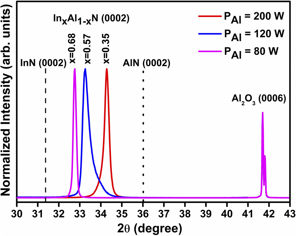 | ||
| Fig. 1 XRD patterns of InxAl1−xN NRs with different In contents (x) grown by MSE using different magnetron powers of the Al target (PAl). | ||
Assuming that all as-grown samples are stress-free, the composition of InxAl1−xN NRs was estimated using Vegard's law given by18,32
| cInxAl1−xN = xcInN + (1 − x)cAlN, | (1) |
 | (2) |
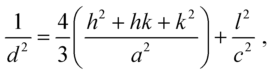
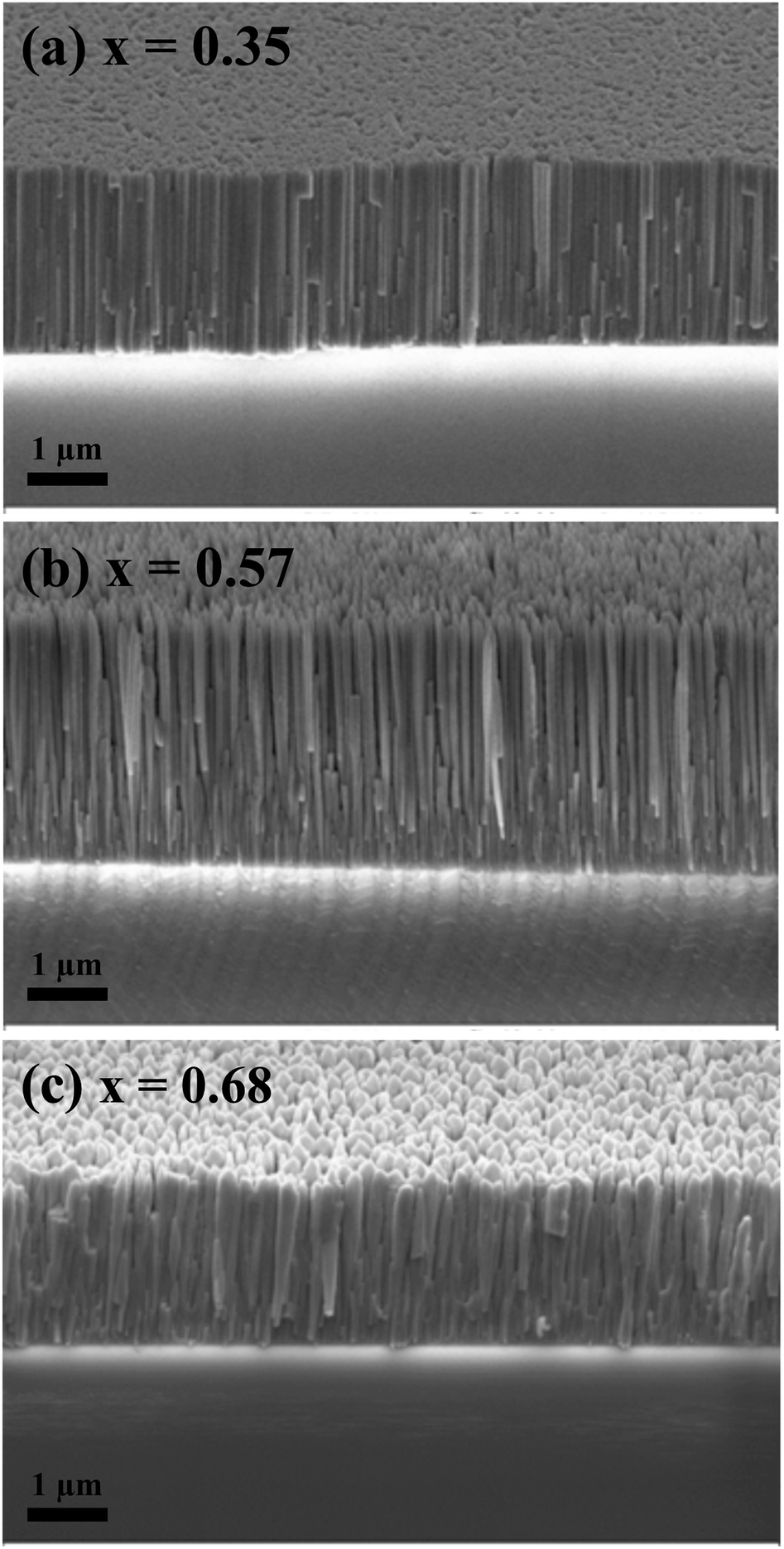
The plan-view SEM images of InxAl1−xN NR samples with different compositions are depicted in Fig. 2. The different InxAl1−xN NRs show similar morphology with highly dense and vertically-aligned NRs on sapphire substrates. STEM-EDX mapping was used to determine the elemental distribution and crystalline structure of the In0.68Al0.32N NR sample as shown in Fig. 3. The cross-sectional STEM image, Fig. 3(a), shows the vertical alignment of NRs and the high-resolution STEM image, Fig. 3(b), shows a clear lattice image confirming the single-crystal quality of the NRs. The EDX elemental mapping, Fig. 3(c), reveals a uniform distribution of elements In, Al, and N across the NRs. No segregation of In-rich or Al-rich clusters is formed in the InxAl1−xN NRs, and no obvious core–shell structure is observed in contrast to the InxAl1−xN NRs reported by Serban et al.34 An EDX line scan was employed to confirm the compositional homogeneity for the cross-sectional In0.68Al0.32N NRs as shown in Fig. 3(d). The line scan section was performed along the yellow dashed line denoted in Fig. 3(c) in which the intensities of both In and Al signals uniformly increase and then decrease in the distance from 0 to 60 nm. The higher intensity denotes higher content of Al and In at the NR core, which is consistent with the cylindrical geometry of the rods. EDX line analysis reveals the uniform distribution of elements Al and In throughout the NR, indicating that the NRs were grown in a single-phase compound rather than a core–shell structure.35
 | ||
| Fig. 2 Plan-view SEM images of InxAl1−xN NRs with different In contents (a) x = 0.35, (b) x = 0.57, and (c) x = 0.68. | ||
 | ||
| Fig. 3 (a) Cross-sectional STEM image, (b) high-resolution STEM image, inset shows a clear lattice image, (c) EDS elemental mapping of Al, In, and N, and (d) EDX line scan of In0.68Al0.32N NRs. | ||
It is known that the energy band gap (Eg) of InxAl1−xN samples depends on the In content in the samples. Hence, it is significant for their applications in optoelectronic devices to calculate the energy band gap of InxAl1−xN samples with different In contents. In accordance with the In content (x), the energy band gap (Eg) of MSE-grown InxAl1−xN can be approximated by following the bowing equation36
| Eg(InxAl1−xN) = 2.28x2 − 4.91x + 4.17. | (3) |
The calculated Eg values are 2.73, 2.11, and 1.88 eV for the samples In0.35Al0.65N, In0.57Al0.43N, and In0.68Al0.32N, respectively. It is observed that the Eg value decreases from 2.73 to 1.88 eV with increase of the In content in the samples from 0.35 to 0.68. The obtained Eg values of InxAl1−xN are in close agreement with the reported values for such alloys.14,31,37,38
Fig. 4 shows the dark current vs. applied voltage (Id–V) measurements of the two terminal single-NR devices with different compositions of In0.35Al0.65N, In0.57Al0.43N, and In0.68 Al0.32N. A typical plan-view SEM image of the NR device is shown in the inset of Fig. 4. The length and width values of the NR were obtained from the SEM image as denoted in the inset figure. For all devices, the Id–V curves reveal linear nature, which suggests good ohmic contact between InxAl1−xN NRs and Pt metal.39,40 The Id–V curves also show that the conductance (G) (i.e. slope) value increases with an increase of indium composition. The electrical conductance (G) defined as G = I/V (ref. 41) can be obtained from the linear fit of the Id–V graph. The slope of the Id–V graph gives the conductance values 2.32 × 10⁻³, 8.00 × 10⁻³, and 1.64 × 10⁻² Ω−1 for the In0.35Al0.65N, In0.57Al0.43N, and In0.68Al0.32N devices, respectively.
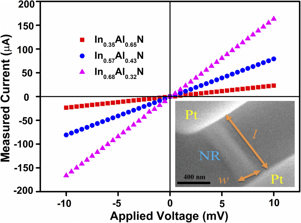 | ||
| Fig. 4 I d–V measurements of InxAl1−xN single-NR devices, where the inset shows a typical SEM image of a FIB-fabricated NR device to measure the length (l) and width (w) of the conduction channel. | ||
The conductivity (σ) of the InxAl1−xN NR devices was calculated from the following relation41
 | (4) |
In Fig. 5 the typical photocurrent response of InxAl1−xN NRs under green light (λ = 532 nm, E = 2.33 eV) illumination at a bias of 0.01 V in air is shown. For all samples, the photocurrent was recorded with different illumination powers (40 to 110 mW). To report photocurrent values, the background dark currents were subtracted from the response curves. The original current response curves under light illumination can be found in ESI Fig. 1.† The results reveal a clear photoresponse of the InxAl1−xN NR devices to the different optical powers. All the photoresponses increase with the increase of power. It is noted that the In0.35Al0.65N NR shows a positive photoresponse and the other two devices (In0.57Al0.43N and In0.68Al0.32N) with higher In composition show a negative photoresponse. A clear transition from conventional positive photoconductivity (PPC) to anomalous negative photoconductivity (NPC) was observed as the In content x increases from 0.35 to 0.68.
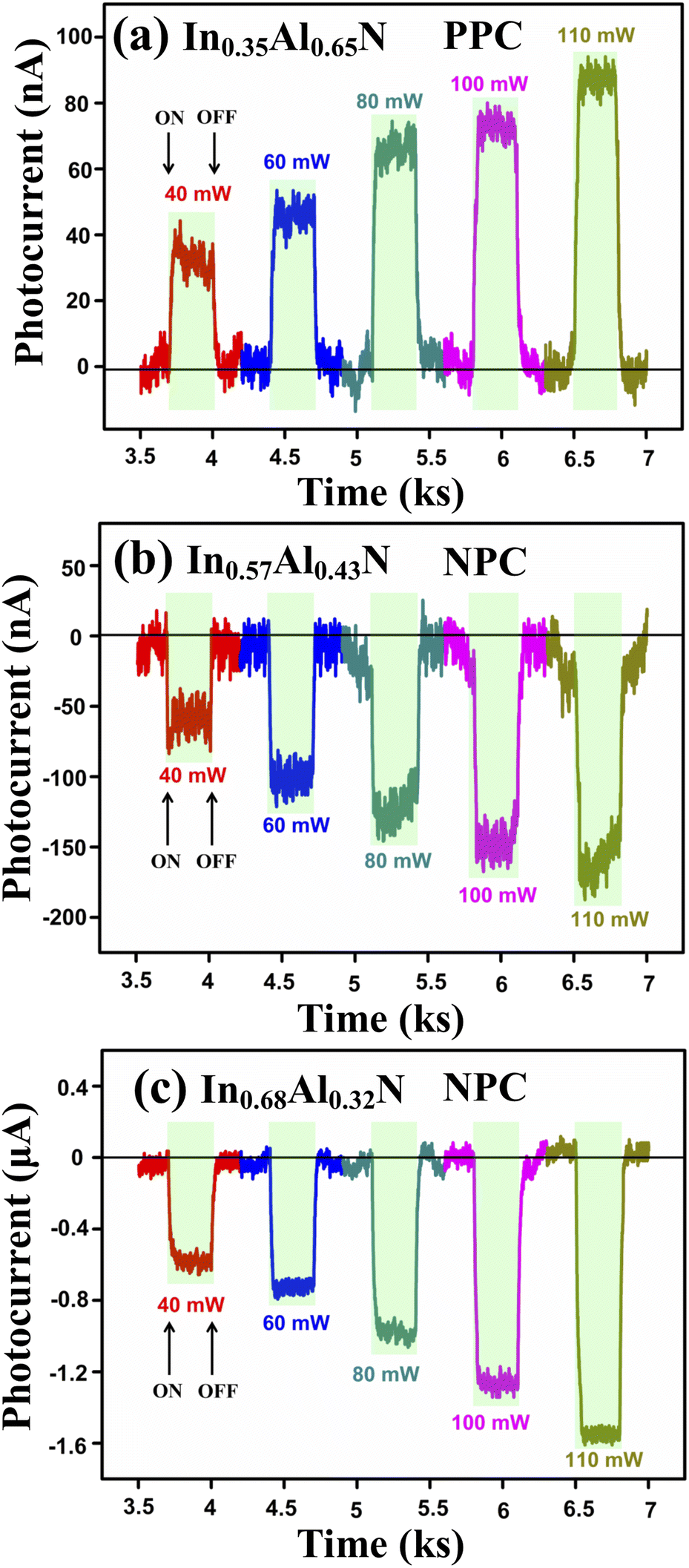 | ||
| Fig. 5 Photocurrent response measurements of InxAl1−xN NR devices under green light illumination with a wavelength of 532 nm and increasing laser power. ON and OFF denote the operation of the laser light source. | ||
The photocurrent vs.light intensity (I) curves for InxAl1−xN NR devices are illustrated in Fig. 6. Optical intensity was obtained from the laser power divided by the laser spot area (diameter ∼ 5 mm). The photocurrent values are linearly dependent on the light intensity for the In0.35Al0.65N NR and inversely dependent on the intensity for In0.57Al0.43N and In0.68Al0.32N NRs. Responsivity (R), a critical parameter determining photodetector performance, is defined as the photocurrent generated by the power of light incident on a photoconductor with an effective area (APC). R can be calculated from the formula43
 | (5) |
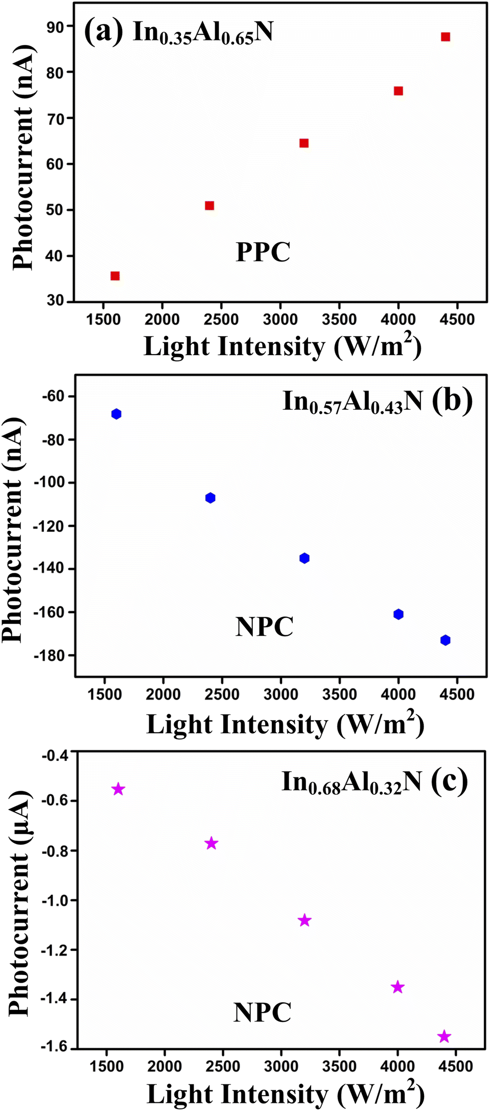 | ||
| Fig. 6 Photocurrent vs. light intensity curves of InxAl1−xN NRs with different In contents (a) x = 0.35, (b) x = 0.57, (c) x = 0.68. | ||
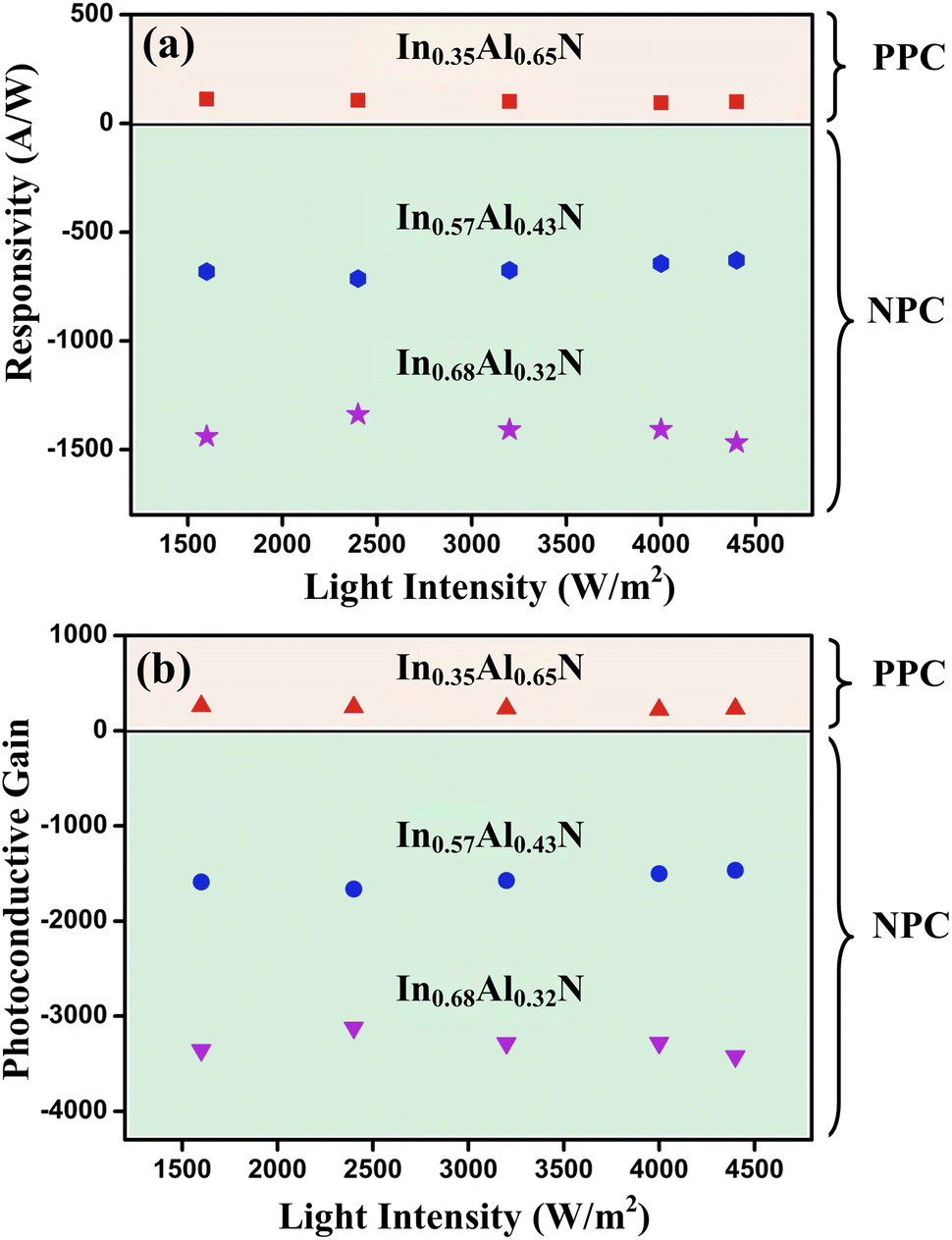 | ||
| Fig. 7 (a) Responsivity and (b) photoconductive gain vs. light intensity of InxAl1−xN NRs with different compositions. | ||
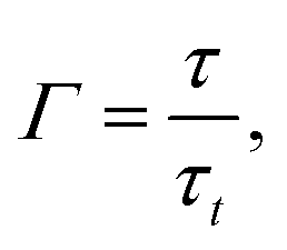
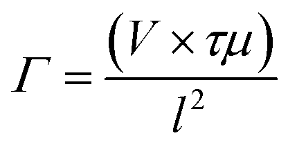
To investigate the physical origin of the high responsivity, photoconductive gain (Γ) was estimated. Γ is a dimensionless parameter and conceptually denotes the number of excess carriers circulating through a photoconductor per unit time before recombination. Therefore, gain is defined as the ratio of carrier lifetime (τ) to transit time (τt) between two electrodes and is written as44,45
 | (6) |
 | (7) |
Γ is also defined as the number of electrons detected per absorbed photon and it is linearly proportional to responsivity and photocurrent, hence the Γ value can be estimated according to the equation48
 | (8) |
The calculated gain vs. intensity curves of the InxAl1−xN NRs are shown in Fig. 7(b). The results show that photoconductive gain (Γ) values are almost constant at different intensities (1600 to 4400 W m−2). The average values of Γ of In0.35Al0.65N, In0.57Al0.43N, and In0.68Al0.32N NRs are 240, −1560, and −3300, respectively. The obtained best responsivity value of the NPC device is compared with those of other NPC devices as listed in Table 1. From the table, it is clear that obtained responsivity of the In0.68Al0.32N NR device is higher than many of the reported values for other NPC photodetectors.
To explain the transition of PPC to NPC in InxAl1−xN NRs, the PC mechanism is demonstrated and proposed for the first time as follows. Generally, band-to-band (or super-bandgap) excitation generates electron–hole pairs (EHPs) as the excess carriers that results in a positive photocurrent. Since the presently used excitation energy (2.33 eV) is lower than the bandgap of the In0.35Al0.65N NR (2.73 eV), the sub-band gap excitation is insufficient for the electrons to be excited from the valence band (VB) to the conduction band (CB) directly. They may, however, follow a two-step process as shown in Fig. 8(a). Electrons are excited from the valence band to the defect bands (such as the electron trap (ET) states) and subsequently to the conduction band (Step 1 and 2 in Fig. 8(a)). The sub-bandgap illumination generates excess EHPs and a positive photocurrent.
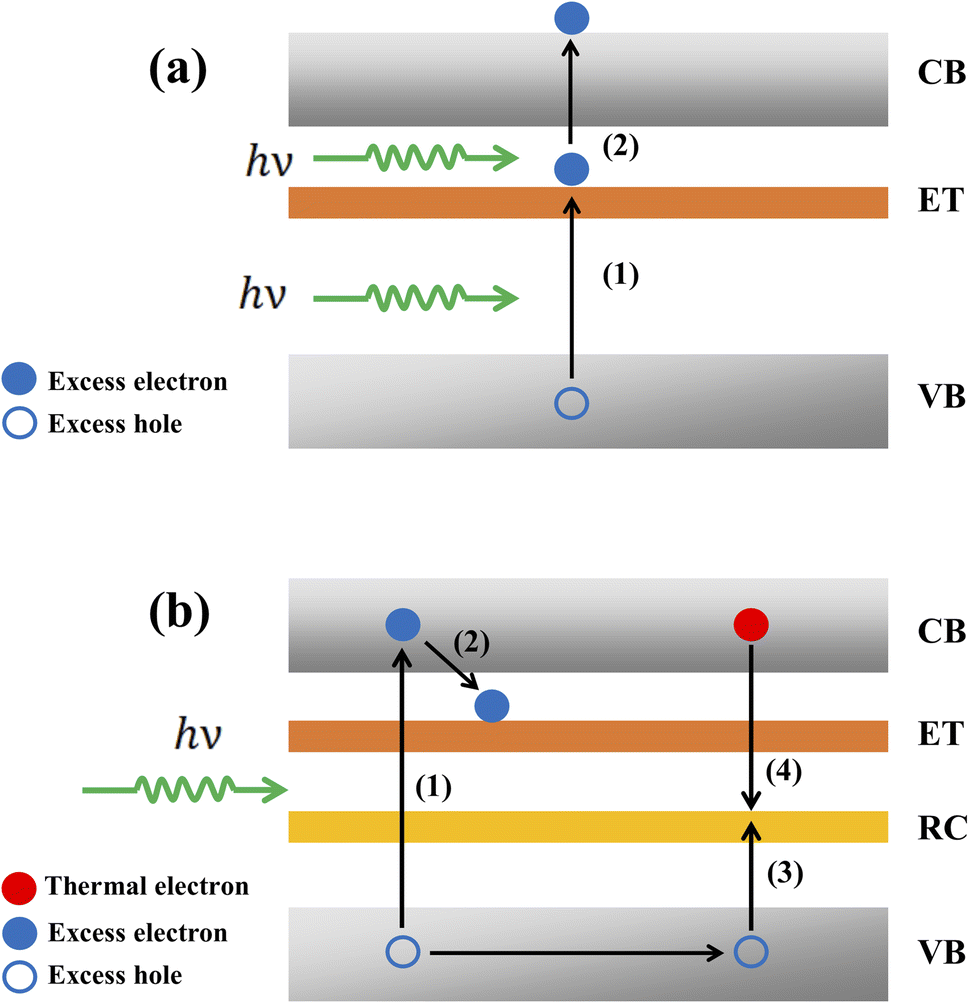 | ||
| Fig. 8 Schematic band diagrams showing transitions involving the (a) PPC mechanism for In0.35Al0.65N NRs and (b) NPC mechanism for In0.57Al0.43N and In0.68Al0.32N NRs. CB denotes the conduction band. VB denotes the valence band. ET denotes electron trap states. RC denotes recombination centers. | ||
Deep electron trap states have been frequently observed in the InAlN films grown by metal–organic chemical vapour deposition.53–55 On increasing the In content from 0.35 to 0.68, it is inferred that more In incorporation could increase the relevant defect density and at the same time could create other imperfection states such as recombination centers (RC) that sometimes originate from the deep acceptor states. The RC or deep acceptors created by high In composition have been previously reported for InAlN films.56,57 Coexistence of the ET and RC could be responsible for the negative photoresponse. The proposed band diagram for the NPC mechanism is shown in Fig. 8(b). In this case, the In-rich In0.57Al0.43N and In0.68Al0.32N NRs have the bandgap (≤2.11 eV) lower than the excitation energy (2.33 eV). The excited electrons could be captured by the ET via the super-bandgap excitation (Steps 1 and 2 in Fig. 8(b)). Subsequently if the unpaired excess holes are also captured by the RC, the positively charged RC will attract thermal electrons (Step 3 and 4 in Fig. 8(b)). Trapping of the thermal electrons lowers the carrier concentration and thus results in a negative photocurrent. This statement explains the transition from PPC to NPC in InxAl1−xN NRs with increasing In composition.
4. Conclusions
Photoconductivity in InxAl1−xN NRs grown by the MSE technique was investigated. The formation of InxAl1−xN NRs was confirmed using XRD, plan-view FESEM, and cross-sectional STEM-EDX techniques. A clear transition from PPC to NPC has been observed in the single-crystalline InxAl1−xN NRs with increasing In content. A model based on the presence of electron trap states and recombination centers is proposed to explain the noted composition-dependent photoconductivity spanning from positive to negative values. The controllable PC characteristics by the MSE process together with the high responsivity and PC gain in the InxAl1−xN NRs demonstrate the potential of ternary nitride 1D nanomaterials for high-performance broad-band photodetectors.Author contributions
Hemanth Kumar Bangolla: methodology, formal analysis, writing/original draft preparation. Ming-Deng Siao: methodology. Yi-Hua Huang: methodology. Ruei-San Chen: supervision, conceptualization, resources, writing/review & editing. Agnė Žukauskaitė: investigation. Justinas Palisaitis: investigation. Per O. Å. Persson: investigation. Lars Hultman: investigation. Jens Birch: investigation. Ching-Lien Hsiao: investigation. All authors discussed the results and approved the final version of the manuscript.Conflicts of interest
The authors declare that there are no conflicts of interest to disclose.Note added after first publication
This article replaces the version published on the 30th of September, which contained an error in eqn (7).Acknowledgements
Author R. S. C. acknowledges the support of the Ministry of Science and Technology. (MOST) of Taiwan (Grant No. MOST 108-2628-M-011-001-MY3, MOST 109-2622-E-011-034, and MOST 110-2622-E-011-017). Author C.-L. H. acknowledges the support of the Swedish Research Council (Grant No. 2018-04198), Swedish Energy Agency (Grant No. 46658-1), and STINT Foundation (Grant No. MG2019-8485). The Swedish Government Strategic Research Area in Materials Science on Functional Materials at Linköping University (Faculty Grant SFO-Mat-LiU 2009-00971) is acknowledged for financial support. The Knut and Alice Wallenberg Foundation is acknowledged for support of the electron microscopy laboratory in Linköping and for project funding (KAW 2020.0033). The Swedish Research Council and the Swedish Foundation for Strategic Research are acknowledged for access to ARTEMI, the Swedish National Infrastructure in Advanced Electron Microscopy (Grant No. 2021-00171 and RIF21-0026).References
- R. B. Chung, F. Wu, R. Shivaraman, S. Keller, S. P. Denbaars, J. S. Speck and S. Nakamura, J. Cryst. Growth, 2011, 324, 163–167 CrossRef CAS.
- F. Wang, S. F. Li, Q. Sun and Y. Jia, Solid State Sci., 2010, 12, 1641–1644 CrossRef CAS.
- R. S. Chen, C. C. Tang, C. L. Hsiao, P. O. Holtz and J. Birch, Appl. Surf. Sci., 2013, 285, 625–628 CrossRef CAS.
- H. Yu, M. H. Memon, D. Wang, Z. Ren, H. Zhang, C. Huang, M. Tian, H. Sun and S. Long, Opt. Lett., 2021, 46, 3271–3274 CrossRef CAS PubMed.
- S. Ali and M. Usman, Eur. Phys. J. Plus, 2022, 137, 1–7 CrossRef PubMed.
- H. Zhang, F. Liang, K. Song, C. Xing, D. Wang, H. Yu, C. Huang, Y. Sun, L. Yang, X. Zhao, H. Sun and S. Long, Appl. Phys. Lett., 2021, 118, 242105 CrossRef CAS.
- P. Nath, A. Biswas and V. Nath, Microsyst. Technol., 2021, 27, 301–306 CrossRef CAS.
- W. C. Chen, Y. H. Wu, C. Y. Peng, C. N. Hsiao and L. Chang, Nanoscale Res. Lett., 2014, 9, 1–7 CrossRef PubMed.
- R. C. Cramer, E. C. H. Kyle and J. S. Speck, J. Appl. Phys., 2019, 126, 035703 CrossRef.
- J. Chen, L. Shen, D. Qi, L. Wu, X. Li, J. Song and X. Zhang, Ceram. Int., 2022, 48, 2802–2810 CrossRef CAS.
- H. Kim-Chauveau, P. DeMierry, J. M. Chauveau and J. Y. Duboz, J. Cryst. Growth, 2011, 316, 30–36 CrossRef CAS.
- N. Hatui, M. Frentrup, A. A. Rahman, A. Kadir, S. Subramanian, M. Kneiss and A. Bhattacharya, J. Cryst. Growth, 2015, 411, 106–109 CrossRef CAS.
- Y. H. Wu, Y. Y. Wong, W. C. Chen, D. S. Tsai, C. Y. Peng, J. S. Tian, L. Chang and E. Y. Chang, Mater. Res. Express, 2014, 1, 015904 CrossRef CAS.
- M. Alizadeh, V. Ganesh, H. Mehdipour, N. F. F. Nazarudin, B. T. Goh, A. Shuhaimi and S. A. Rahman, J. Alloys Compd., 2015, 632, 741–747 CrossRef CAS.
- W. Lv, L. Shen, J. Liu, J. Chen, L. Wu, D. Qi, G. Zhang and X. Li, Appl. Surf. Sci., 2020, 504, 144335 CrossRef CAS.
- H. F. Liu, C. G. Li, K. K. Ansah Antwi, S. J. Chua and D. Z. Chi, Mater. Lett., 2014, 128, 344–348 CrossRef CAS.
- J. Palisaitis, C. L. Hsiao, L. Hultman, J. Birch and P. O. Å. Persson, Acta Mater., 2013, 61, 4683–4688 CrossRef CAS.
- C. J. Dong, M. Xu, Q. Y. Chen, F. S. Liu, H. P. Zhou, Y. Wei and H. X. Ji, J. Alloys Compd., 2009, 479, 812–815 CrossRef CAS.
- T. Peng, J. Piprek, G. Qiu, J. O. Olowolafe, K. M. Unruh, C. P. Swann and E. F. Schubert, Appl. Phys. Lett., 1997, 71, 2439–2441 CrossRef CAS.
- K. Sato, J. Ohta, S. Inoue, A. Kobayashi and H. Fujioka, Appl. Phys. Express, 2009, 2, 0110031–0110033 Search PubMed.
- K. Ueno, A. Kobayashi, J. Ohta, H. Fujioka, H. Amanai, S. Nagao and H. Horie, Phys. Status Solidi RRL, 2009, 3, 58–60 CrossRef CAS.
- C. L. Hsiao, J. Palisaitis, M. Junaid, P. O. Å. Persson, J. Jensen, Q. X. Zhao, L. Hultman, L. C. Chen, K. H. Chen and J. Birch, Thin Solid Films, 2012, 524, 113–120 CrossRef CAS.
- N. A. A. Zulkifli, K. Park, J. W. Min, B. S. Ooi, R. Zakaria, J. Kim and C. L. Tan, Appl. Phys. Lett., 2020, 117, 191103 CrossRef CAS.
- S. Ju, K. Lee, M. H. Yoon, A. Facchetti, T. J. Marks and D. B. Janes, Nanotechnology, 2007, 18, 155201 CrossRef.
- D. Wang, C. Huang, X. Liu, H. Zhang, H. Yu, S. Fang, B. S. Ooi, Z. Mi, J. H. He and H. Sun, Adv. Opt. Mater., 2021, 9, 1–8 Search PubMed.
- S. Kang, R. Nandi, H. Kim, K. U. Jeong and C. R. Lee, J. Mater. Chem. C, 2018, 6, 1176–1186 RSC.
- D. Wang, X. Liu, Y. Kang, X. Wang, Y. Wu, S. Fang, H. Yu, M. H. Memon, H. Zhang, W. Hu, Z. Mi, L. Fu, H. Sun and S. Long, Nat. Electron., 2021, 4, 645–652 CrossRef CAS.
- W. Lu, N. Nakayama, K. Ito, S. Katsuro, N. Sone, Y. Miyamoto, K. Okuno, M. Iwaya, T. Takeuchi, S. Kamiyama and I. Akasaki, ACS Appl. Mater. Interfaces, 2021, 13, 54486–54496 CrossRef CAS PubMed.
- A. Fan, Z. Zhuang, X. Zhang, C. Li, H. Jiang, S. Chen, X. Luo, G. Hu and Y. Cui, J. Alloys Compd., 2021, 885, 161166 CrossRef CAS.
- D. Ji, B. Ercan, G. Benson, A. K. M. Newaz and S. Chowdhury, Appl. Phys. Lett., 2020, 116, 211102 CrossRef CAS.
- A. Núñez-Cascajero, S. Valdueza-Felip, L. Monteagudo-Lerma, E. Monroy, E. Taylor-Shaw, R. W. Martin, M. González-Herráez and F. B. Naranjo, J. Phys. D: Appl. Phys., 2017, 50, 065101 CrossRef.
- N. Afzal, M. Devarajan and K. Ibrahim, J. Alloys Compd., 2015, 652, 407–414 CrossRef CAS.
- Z. Dridi, B. Bouhafs and P. Ruterana, Semicond. Sci. Technol., 2003, 18, 850–856 CrossRef CAS.
- E. A. Serban, P. O. Å. Persson, I. Poenaru, M. Junaid, L. Hultman, J. Birch and C. L. Hsiao, Nanotechnology, 2015, 26, 215602 CrossRef PubMed.
- C. L. Hsiao, J. Palisaitis, M. Junaid, R. S. Chen, P. O. Å. Persson, P. Sandstrom, P. O. Holtz, L. Hultman and J. Birch, Appl. Phys. Express, 2011, 4, 115002 CrossRef.
- J. J. Chen, D. L. Qi, X. F. Li, J. Y. Song and L. H. Shen, Appl. Phys. A: Mater. Sci. Process., 2022, 128, 1–8 CrossRef.
- W. Song, T. Li, L. Zhang, W. Zhu and L. Wang, J. Alloys Compd., 2021, 885, 160977 CrossRef CAS.
- M. Alizadeh, V. Ganesh, A. Pandikumar, B. T. Goh, S. Azianty, N. M. Huang and S. A. Rahman, J. Alloys Compd., 2016, 670, 229–238 CrossRef CAS.
- M. D. Siao, W. C. Shen, R. S. Chen, Z. W. Chang, M. C. Shih, Y. P. Chiu and C. M. Cheng, Nat. Commun., 2018, 9, 1442 CrossRef CAS PubMed.
- H. W. Yang, H. F. Hsieh, R. S. Chen, C. H. Ho, K. Y. Lee and L. C. Chao, ACS Appl. Mater. Interfaces, 2018, 10, 5740–5749 CrossRef CAS PubMed.
- Y. H. Huang, R. S. Chen, J. R. Zhang and Y. S. Huang, Nanoscale, 2015, 7, 18964–18970 RSC.
- S. Surender, S. Pradeep, K. Prabakaran, S. M. Sumithra, S. Singh and K. Baskar, J. Alloys Compd., 2018, 734, 48–54 CrossRef CAS.
- M. Anandan, H. F. Hsieh, F. C. Liu, C. Y. Chen, K. Y. Lee, L. C. Chao, C. H. Ho and R. S. Chen, Nanotechnology, 2020, 31, 465201 CrossRef CAS PubMed.
- P. Bhattacharya, Semiconductor Optoelectronic Devices, Prentice-Hall Inc., New Jersey, 1997, Chap. 8, pp. 346–348 Search PubMed.
- M. Razeghi and A. Rogalski, J. Appl. Phys., 1996, 79, 7433–7473 CrossRef CAS.
- R. S. Chen, H. Y. Tsai, Y. S. Huang, Y. T. Chen, L. C. Chen and K. H. Chen, Appl. Phys. Lett., 2012, 101, 113109 CrossRef.
- R. S. Chen, C. A. Chen, H. Y. Tsai, W. C. Wang and Y. S. Huang, J. Phys. Chem. C, 2012, 116, 4267–4272 CrossRef CAS.
- F. González-Posada, R. Songmuang, M. Den Hertog and E. Monroy, Nano Lett., 2012, 12, 172–176 CrossRef PubMed.
- B. H. Kim, S. H. Kwon, H. H. Gu and Y. J. Yoon, Phys. E, 2019, 106, 45–49 CrossRef CAS.
- L. Xie, L. Guo, W. Yu, T. Kang, R. K. Zheng and K. Zhang, Nanotechnology, 2018, 29, 464002 CrossRef PubMed , 0–7.
- Q. Wang, Y. Tu, T. Ichii, T. Utsunomiya, H. Sugimura, L. Hao, R. Wang and X. He, Nanoscale, 2017, 9, 14703–14709 RSC.
- S. Ratha, A. J. Simbeck, D. J. Late, S. K. Nayak and C. S. Rout, Appl. Phys. Lett., 2014, 105, 243502 CrossRef.
- Z. Chen, K. Fujita, J. Ichikawa, Y. Sakai and T. Egawa, Jpn. J. Appl. Phys., 2011, 50, 081001 CrossRef.
- M. A. Py, L. Lugani, Y. Taniyasu, J. F. Carlin and N. Grandjean, Phys. Rev. B: Condens. Matter Mater. Phys., 2014, 90, 115208 CrossRef , 1–13.
- D. Johnstone, J. H. Leach, V. A. Kovalskii, Q. Fan, J. Xie and H. Morkoç, Gall. Nitride Mater. Devices IV, 2009, 7216, 72162R Search PubMed.
- R. E. Jones, S. X. Li, K. M. Yu, J. W. Ager, E. E. Haller, W. Walukiewicz, H. Lu and W. J. Schaff, J. Phys. D: Appl. Phys., 2009, 42, 095406 CrossRef.
- P. Chauhan, S. Hasenöhrl, E. Dobročka, L. Vančo, R. Stoklas, J. Kováč, P. Šiffalovič and J. Kuzmík, Appl. Surf. Sci., 2019, 470, 1–7 CrossRef CAS.
Footnote |
| † Electronic supplementary information (ESI) available. See https://doi.org/10.1039/d2na00456a |
| This journal is © The Royal Society of Chemistry 2022 |