
 Open Access Article
 This Open Access Article is licensed under a
 Creative Commons Attribution 3.0 Unported Licence
Recent progress in one dimensional TiO2 nanomaterials as photoanodes in dye-sensitized solar cells
Deepak
Joshy
a,
Soumya B.
Narendranath
b,
Yahya A.
Ismail
 a and
Pradeepan
Periyat
*c
a and
Pradeepan
Periyat
*c
aDepartment of Chemistry, University of Calicut, Kerala 673635, India
bDepartment of Chemistry, Central University of Kerala, 671316, India
cDepartment of Environmental Studies, Kannur University, Kerala, India. E-mail: pperiyat@kannuruniv.ac.in
First published on 30th September 2022
Abstract
Exploiting the vast possibilities of crystal and electronic structural modifications in TiO2 based nanomaterials creatively attracted the scientific community to various energy applications. A dye sensitised solar cell, which converts photons into electricity, is considered a viable solution for the generation of electricity. TiO2 nanomaterials were well accepted as photoanode materials in dye-sensitized solar cells, and possess non-toxicity, high surface area, high electron transport rates, fine tuneable band gap, high resistance to photo corrosion and optimum pore size for better diffusion of dye and electrolyte. This review focuses on various aspects of TiO2 nanomaterials as photoanodes in dye-sensitized solar cells. TiO2 photoanode modification via doping and morphological variations were discussed in detail. The impact of various morphologies on the design of TiO2 photoanodes was particularly stressed.
 Deepak Joshy | Mr Deepak Joshy is presently working as a Senior Research Fellow under the CSIR-UGC JRF scheme in the Department of Chemistry, University of Calicut under the guidance of Dr Pradeepan Periyat. His research mainly focuses on the design and development of nanomaterials for energy saving and environmental applications. His major research areas are photocatalysts and adsorbents for water purification, inorganic pigments for cool coatings and supercapacitors. |
 Soumya B. Narendranath | Dr Soumya B. Narendranath is currently a post-doctoral fellow in the Department of Chemistry, Central University of Kerala, India. She obtained her PhD degree from CSIR-National Chemical Laboratory (NCL), Pune, where she studied photocatalytic water splitting activity of layered metal oxides. She is the recipient of the SERB-National Post-Doctoral Fellowship and Dr D. S. Kothari-UGC Fellowship. She has completed two post-doctoral fellowships at Central University of Kerala. Her research interests include design and development of metal oxide nanoparticles for solar energy utilization and heterogeneous catalysis for biomass conversion. |
 Yahya A. Ismail | Dr Yahya A. Ismail received his PhD from Aligarh Muslim University (AMU), India. He joined as a Reader in Chemistry at University of Calicut in 2005. Then he worked as a CRI researcher at the Center for Bio artificial Muscles, Hanyang University, South Korea. Later, he served as a faculty member in University of Nizwa and Al Sharqiyah University, Oman. Presently, he is working as an Associate Professor of Chemistry, University of Calicut, India. His research is focused on conducting polymer-based artificial muscles and sensors, electrochemical super capacitors and stimuli responsive polymers. |
 Pradeepan Periyat | Dr Pradeepan Periyat is currently working as an Associate Professor and Head, Department of Environmental Studies, Mangattuparamba Campus, Kannur University, Kerala, India. He completed two post doctoral fellowships at University of Limerick, Ireland and Monash University, Melbourne, Australia. He was awarded the prestigious Marie-Curie Fellowship from 2009 to 2012. He is an Associate Member of the Royal Society of Chemistry (RSC), London. He received the Young Scientist Award 2017 from KSCSTE, Kerala State Government. He has published 60 scientific articles in leading peer reviewed journals and 12 book chapters. His research group focuses on nanomaterials synthesis for energy and environmental applications. |
1. Introduction
The excessive consumption of fossil fuels to meet the increasing energy demand has resulted in profound consequences such as global warming, environmental pollution, etc. To address the challenges raised by environmental degradation and the energy crisis, the development of a sustainable energy production approach is required. Even though various renewable energy resources such as geothermal energy, biofuels, and wind-tidal energies can substantially contribute to sustainable energy development, solar energy has to play a major role. In this era of growing energy demand and environmental issues, solar energy is the only choice left in front of us as solar radiation possesses immense potential, vast abundance and environmental friendliness. Out of the 4 million exajoules (1018 J) of solar energy reaching the earth, around 50![[thin space (1/6-em)]](https://www.rsc.org/images/entities/char_2009.gif) 000 EJ's are easily exploitable.1 The significance of solar energy becomes more clear from the fact that the world's annual energy consumption for the year 2017 was around 565 EJ's which is only a fraction of the harvestable solar energy (i.e. 50000 EJ's).2 But in the present scenario, electricity produced from the renewable energy sector constitutes only 8.4% of the total world electricity production.2 More than 20% of the contribution to the renewable energy sector is made by solar energy.3 But this share of solar energy is significantly small compared to the magnitude of solar power available for harvesting. The lack of efficient and economically viable solar harvesting techniques is the main reason for this huge difference. Solar cells are one of the widely employed solar energy conversion devices. Solar cells are classified into different generations based on the material and technology present in them. We have first generation silicon solar cells as the most widely commercialized solar cell type.4,5 Silicon solar cells have efficiencies of around 26% which is almost near the theoretical efficiency maximum.6 At the same time, second-generation solar cells are based on thin-film technology and employ materials such as CdTe, CIGS, etc.7–10 The efficiency of second-generation solar cells has reached up to 21.7% recently.6 But the large-scale commercialization of first and second-generation solar cells is very expensive. Also, the components used in these two generations are capable of causing environmental hazards. So, to develop an economically viable and eco-friendly way of solar energy conversion, the third generation of solar cells, known as dye-sensitized solar cells (DSSCs) was introduced.11–14 The concept of a DSSC was introduced by Michael Gratzel in 1991.15 Significant attraction garnered by DSSCs is due to their large-scale and economically viable production capability along with flexibility. The efficiencies of DSSCs introduced so far are found to be within 14.3%.16 If the issues associated with low efficiency and shorter durability are addressed properly, DSSCs are the best to play a vital role in the development of a sustainable energy culture. Also, large-scale commercialization of DSSCs can convert a major share of the available solar radiation. Performance enhancement, durability increment and production cost reduction of DSSCs can be carried out in various ways. Mainly it involves either the synthesis of novel component materials/modification of existing materials or the introduction of more rational DSSC designs. As a DSSC assembly consists of various components such as a photoanode, sensitizer(dye), counter electrode, redox electrolyte, etc., investigation into performance enhancement can be carried out on any one of these components. In this review, special emphasis is given to the DSSC photoanode and the contribution of one dimensional TiO2 nanomaterial based photoanodes for the critical development of DSSCs.
000 EJ's are easily exploitable.1 The significance of solar energy becomes more clear from the fact that the world's annual energy consumption for the year 2017 was around 565 EJ's which is only a fraction of the harvestable solar energy (i.e. 50000 EJ's).2 But in the present scenario, electricity produced from the renewable energy sector constitutes only 8.4% of the total world electricity production.2 More than 20% of the contribution to the renewable energy sector is made by solar energy.3 But this share of solar energy is significantly small compared to the magnitude of solar power available for harvesting. The lack of efficient and economically viable solar harvesting techniques is the main reason for this huge difference. Solar cells are one of the widely employed solar energy conversion devices. Solar cells are classified into different generations based on the material and technology present in them. We have first generation silicon solar cells as the most widely commercialized solar cell type.4,5 Silicon solar cells have efficiencies of around 26% which is almost near the theoretical efficiency maximum.6 At the same time, second-generation solar cells are based on thin-film technology and employ materials such as CdTe, CIGS, etc.7–10 The efficiency of second-generation solar cells has reached up to 21.7% recently.6 But the large-scale commercialization of first and second-generation solar cells is very expensive. Also, the components used in these two generations are capable of causing environmental hazards. So, to develop an economically viable and eco-friendly way of solar energy conversion, the third generation of solar cells, known as dye-sensitized solar cells (DSSCs) was introduced.11–14 The concept of a DSSC was introduced by Michael Gratzel in 1991.15 Significant attraction garnered by DSSCs is due to their large-scale and economically viable production capability along with flexibility. The efficiencies of DSSCs introduced so far are found to be within 14.3%.16 If the issues associated with low efficiency and shorter durability are addressed properly, DSSCs are the best to play a vital role in the development of a sustainable energy culture. Also, large-scale commercialization of DSSCs can convert a major share of the available solar radiation. Performance enhancement, durability increment and production cost reduction of DSSCs can be carried out in various ways. Mainly it involves either the synthesis of novel component materials/modification of existing materials or the introduction of more rational DSSC designs. As a DSSC assembly consists of various components such as a photoanode, sensitizer(dye), counter electrode, redox electrolyte, etc., investigation into performance enhancement can be carried out on any one of these components. In this review, special emphasis is given to the DSSC photoanode and the contribution of one dimensional TiO2 nanomaterial based photoanodes for the critical development of DSSCs.
1.1. DSSC structure & working- an overview
A photoanode forms the core part of the DSSC and it consists of a transparent conducting oxide (TCO) glass plate or plastic substrate on which nanometre-sized semiconducting metal oxide particles are deposited and sintered. Fluorine-doped tin oxide (FTO) is the most widely employed substrate.17,18 Usually, a mesoporous TiO2 film having a thickness of around 10 µm is coated on the FTO substrate to facilitate electron transfer.19 Sensitizer or dye molecules responsible for light absorption are adsorbed onto the mesoporous nanomaterial film. Upon irradiation by solar radiation, the dye molecule will get excited and emit an electron. This emitted electron will get injected into the conduction band of the nanocrystalline semiconductor metal oxide film. From there the electron will get transferred to the FTO plate and then to the external circuit. The dye molecule which got oxidised on solar irradiation is now regenerated by employing a redox couple.20,21 The iodide/triiodide redox system is the most widely used one.22 Upon reduction of the oxidised dye molecule, the iodide ion gets oxidised into triiodide. The regeneration of the redox couple is facilitated by electrons which reach the counter electrode through the external circuit. The counter electrode consists of a thin layer of Pt nanoparticles deposited on a conducting glass substrate.23,24 Here the electron emitted from the dye molecule travels through the mesoporous nanomaterial layer deposited on the FTO plate and then flows through the external load and finally reaches the counter electrode to regenerate the redox system. The redox electrolyte system present in between the two electrodes not only facilitates dye regeneration but also prevents the recombination of conduction band electrons with oxidised dye molecules. While fabricating the DSSC, as shown in Fig. 1 the photoanode and cathode are sandwiched together with a layer of the polymer film in between them.25 Then the redox electrolyte system is injected into the space in between so that the triiodide ions can diffuse towards the counter electrode and get reduced to iodide ions. A number of such repeating cycles produce current in the circuit. The resultant efficiency of a DSSC depends on the electron recombination rate. The lower the electron recombination rate, the higher the efficiency will be. The lower electron recombination rate results from the high electron transport rate.26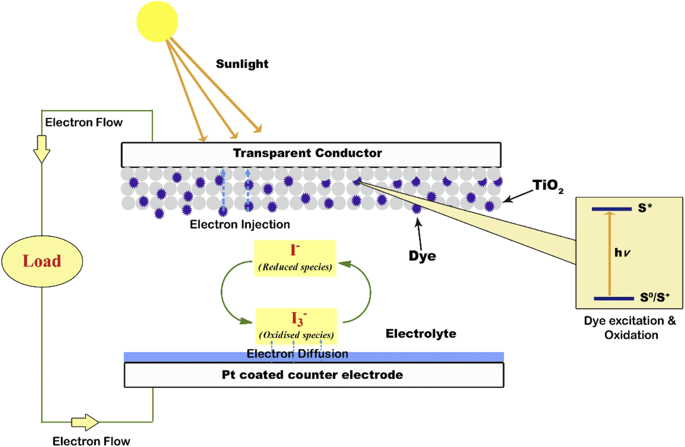 | ||
| Fig. 1 Schematic diagram of a DSSC. | ||
1.2. Important terms associated with DSSCs
The important parameters associated with dye sensitised solar cells are incident photon-to-current efficiency (IPCE), open circuit voltage (VOC), short circuit current (Jsc), fill factor (FF) and cell efficiency.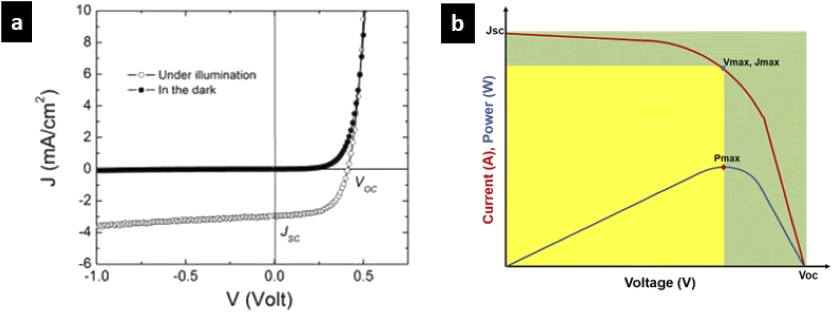 | ||
| Fig. 2 (a) The current versus voltage curve associated with a solar cell circuit in the dark and under illumination (Copyright: https://depts.washington.edu/). (b) Graphical representation of the fill factor. | ||
A higher fill factor favours the maximum output of a solar cell. The graphical representation of the fill factor is shown in Fig. 2b. This graph shows the solar cell output current and power as a function of voltage. It is the ratio of the area of the larger rectangle (pale green) to the area of the smaller rectangle (yellow).
| Pmax = Voc × Jsc × FF |
| η = Voc × Jsc × FF/Pin |
1.3. Role of the photoanode in a DSSC
Among the functional components of a DSSC, the photoanode forms the crucial part. The nature of the material used as the photoanode and its morphology are important factors determining the overall performance of a DSSC. The functions of a photoanode include dye pickup, electron injection, transportation and collection which in turn influence the photocurrent, photovoltage and power conversion efficiency. Efforts are being made to improve the efficiency of DSSCs by introducing novel materials as photoanodes and by modifying the morphologies of existing materials. The essential requirements for an ideal photoanode are:(i) Higher surface area facilitates the adsorption of dye molecules to a greater extent.31,32
(ii) Photoanodes should have higher electron transport rates so that the electron injection from the dye to the external circuit through the photoanode occurs smoothly.33
(iii) Photoanodes should have suitable band gap alignment with the energy levels of the sensitizer.34
(iv) It should possess high resistance to photo corrosion.35
(v) Photoanode materials should possess a pore size that can be optimized to achieve better diffusion of dye and electrolyte.36
(vi) It should possess the ability to absorb/scatter sunlight for the improved performance of the dye.37
(vii) The photoanode material needs to be in optimum contact with the dye molecules and the conducting substrate.38
The above-mentioned characteristics are vital in achieving a better photoconversion efficiency.
This review discusses the significance of TiO2 nanomaterials as photoanodes in DSSCs. The characteristic photovoltaic properties and important modifications of TiO2 for photoanode applications are surveyed. A summary of research on TiO2 and its important one-dimensional morphologies and their modifications to be used as photoanode materials in DSSCs is given here.
2. Photoanode materials
The limitations associated with the conventional materials lead to the investigation of more effective photoanode materials, which have advanced properties with bulk and surface modifications. Commonly investigated materials include metal oxides such as TiO2, ZnO,39–42 Nb2O5,43–45 SnO2,46–48 SrTiO3,49,50 WO3,51–53 and Zn2SnO4.54–56 All these are wide band gap semiconductor materials whose structure, morphology and crystallinity decide the performance of the DSSCs. The band structures of these materials are shown in Fig. 3.57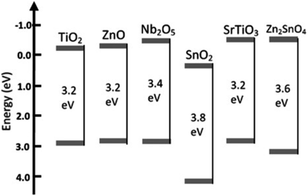 | ||
| Fig. 3 Band positions of various semiconductor oxide materials used as photoanodes.57 (Reprinted with permission from ref. Yang et al., 2013. Copyright 2013 WILEY‐VCH Verlag GmbH & Co. KGaA, Weinheim.) | ||
Among these materials, TiO2 and ZnO are the most widely used materials for DSSC fabrication.58–62 Although ZnO has better electron mobility compared to TiO2, its efficiency is less than those DSSCs employing TiO2. This lower efficiency of ZnO emerges due to decreased dye adsorption and instability in acidic environments.63 Therefore, TiO2 has superior photovoltaic applicability compared to ZnO. Four polymorphs of TiO2 are known, viz, as rutile (tetragonal), anatase (tetragonal), brookite (orthorhombic) and TiO2 (B) (monoclinic) as shown in Fig. 4.64–66 Among these polymorphs of TiO2, anatase is preferred over rutile for photovoltaic applications irrespective of rutile's greater stability and lower band gap. This is because the anatase phase has a higher conduction band energy level, absorptive affinity and a lower electron–hole recombination rate.67 Since the synthesis of brookite TiO2 is difficult, its applicability as a photoanode remains less explored.68
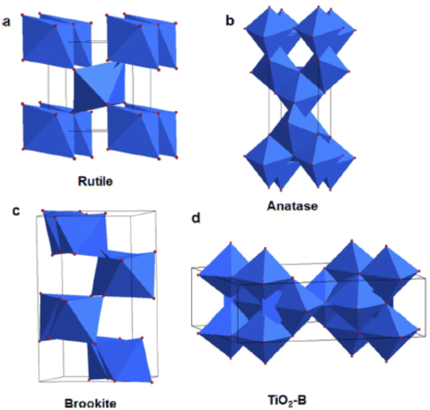 | ||
| Fig. 4 Schematic unit cell structure of four TiO2 polymorphs: (a) rutile (b) anatase (c) brookite and (d) TiO2 (B)66 (Reprinted with permission from ref. Wang, X. et al., 2014. Copyright 2014 American Chemical Society). | ||
DSSCs employing anatase TiO2 showed efficiencies ranging from 12–14%.69,70 So TiO2 is considered the best choice available as a photoanode material due to its (a) cost-effectiveness, (b) easy availability, (c) good stability along with non-toxicity and (d) suitable optical and electronic characteristics.67 Furthermore, most of the stable sensitizers showing higher light absorption capability have their LUMO positioned favourably with the conduction band of TiO2. These favourable qualities of TiO2 initiated further investigations to improve the functioning of TiO2 photoanodes. During this process of improvement, the main challenges to deal with include the (i) large band gap (3.2 eV) of TiO2 causing adsorption in the UV region71 and (ii) low internal electron transport rate.72 Furthermore, research aimed at better performance of TiO2 by focusing on factors such as high surface area, an increased light scattering effect, enhanced interface quality, fast electron mobility and better charge collection ability. The physical, chemical and optical properties of TiO2 depend not only on its intrinsic electronic structure but also on its shape, size, porosity, pore size distribution, organization and surface features. One approach to increase the photoconversion efficiency is by maximising the surface area of TiO2 and thereby enhancing the reaction at the interface of the photoanode and interacting media. The extent of dye adsorption depends on the surface area available. The greater the dye pickup, the more the electron/current density that will be generated. Semiconductor mesoporous TiO2 (Fig. 5), nanorods (Fig. 6a and b), nanowires (Fig. 6c and d), nanotubes (Fig. 6e), nanosheets and various other nanoarchitectures have been employed and explored for enhanced dye adsorption.73–76 Besides increasing the surface area, enhancing electron mobility is also a crucial factor in improving the performance of the photoanode. Defects in TiO2 act as electron traps at the grain boundaries and the absence of defects will assure better collection of injected electrons from the semiconductor. Another method involves surface modification of TiO2 semiconductors which has remarkable influence on charge separation, electron mobility and the recombination process.77 Attempts are being made to minimise electron recombination losses due to grain boundaries and also to extend the absorption of TiO2 towards the near-infrared region.
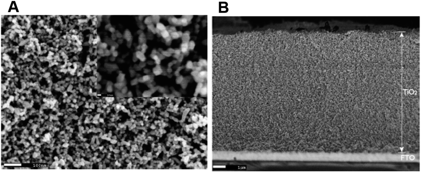 | ||
| Fig. 5 (a) SEM images of mesoporous TiO2 and (b) film thickness of mesoporous TiO273 (Reprinted with permission from ref. Muniz et al., 2011. Copyright 2010 Elsevier). | ||
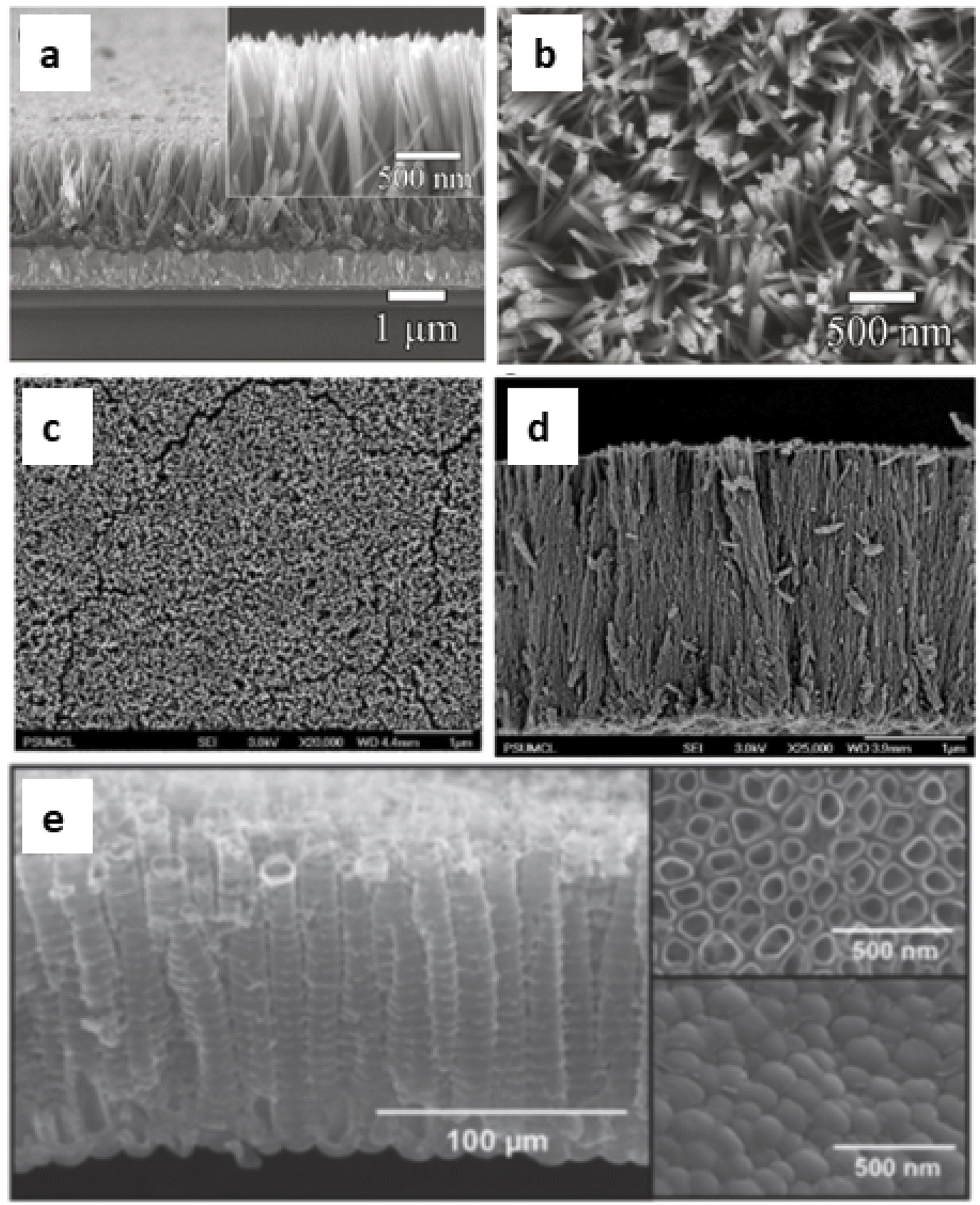 | ||
| Fig. 6 SEM images: (a) cross sectional view and (b) top view of TiO2 nanorods74 (Reprinted with permission from ref. Cho et al., 2011. Copyright 2011 American Chemical Society); FESEM images (c) top view images and (d) cross sectional image of a TiO2 nanowire array on FTO coated glass75 (Reprinted with permission from ref. Feng et al., 2008. Copyright 2008 American Chemical Society) and (e) SEM images of TiO2 nanotubes76 (Reprinted with permission from ref. Roy et al., 2010. Copyright 2009 Royal Society of Chemistry). | ||
2.1. TiO2 photoanode modification by doping
Electronic properties of TiO2 can be effectively modified by doping i.e. by the deliberate insertion of impurities into the TiO2 lattice.78 Doping in the TiO2 lattice results in an increase in free charge carriers and conductivity.79 This is due to the defect-ridden nature of TiO2 and it influences the electronic structure and trap states present in the lattice.80 While doping, either the Ti4+ cation or O2− anion can be replaced. TiO2 has a band structure consisting of conduction band (CB) energy levels formed by the Ti4+ orbitals and valence band (VB) energy levels comprised of O2− 2p orbitals.67 Thus replacing Ti4+ and O2− ions will alter the CB and VB structures respectively.81 The atomic radii of the dopants should be comparable to the ions to be replaced.82 The sensitizer dye molecules used to bind with Ti atoms in the TiO2 lattice and the replacement of Ti with other atoms will affect the dye adsorption due to different binding strengths between the dye and the dopant.83,84 It was also observed that the growth rate of TiO2 nanoparticles is inhibited by dopants resulting in smaller particles having increased surface area.85,86 As a result of an increase in surface area, dye adsorption and current densities are improved.87 This will automatically enhance light absorption and facilitate the use of thinner films having a lower recombination rate in DSSCs.32Various morphologies of TiO2 have a major influence on its optical and electronic properties.88 It is found that one-dimensional nanostructures such as nanowires, nanorods and nanotubes possess better charge transport properties compared to nanoparticle assemblies.89 However, these 1D structures have lesser surface area than nanoparticle systems and thereby have reduced dye pick-up capability.90 Dopants having better dye adsorption capacities can improve the photovoltaic performance of 1D nanostructures.91,92 At the same time, nanoparticle assemblies benefit from dopants that cause increased charge transfer.93 Hence, it is difficult to identify clearly whether performance improvement is caused by an increase in absorption or electronic effects in doped TiO2.
Based on the general electronic configuration, dopants can be classified into alkaline earth metals,94–96 metalloids,97–99 non-metals,100–102 transition metals,103 post-transition metals104,105 and lanthanides.106–108 Significant attempts were made for co-doping in which more than one dopant is introduced into the lattice for enhanced device performance.109–111 Doping in a TiO2 lattice alters its phase, flat band potential, recombination rate, electron transport rate and dye adsorption capability.79 Anatase to rutile phase transformation is inhibited by doping,112 thereby reducing charge carrier recombination. The flat band potential will experience either a positive or a negative shift i.e. a positive shift involves the downward shift of the CB and Fermi level (EF) whereas a negative shift involves the upward shift of the CB and EF. A decrease in the number of defect states upon doping increases the lifetime of photogenerated electrons and reduces recombination losses.113 At the same time, a decrease in the number of trap states may lead to enhanced electron mobility.114 Dopants influence the growth rate of nanoparticles, thereby affecting their size, surface area and the number of grain boundaries. Also, dopants decide the binding strength between the doped surface and dye molecules.115 Recently, Mn-doped TiO2 with IR absorbing capability was reported to be an excellent photoanode for dye-sensitized solar cells and it possesses 79% higher efficiency compared to commercial P25.116
2.2. Nanostructured TiO2 photoanode
A revolutionary breakthrough in the field of photoanode fabrication with the introduction of a mesoporous TiO2 nanoparticle photoanode was pioneered by Gratzel and co-workers in 1991.117 They replaced the bulk TiO2 photoelectrode with a nanostructured architecture and obtained an efficiency of 7.1–7.9% by employing a trimeric Ru complex.118 Detailed guidelines for the fabrication of a TiO2 nanoelectrode for DSSCs with efficiency >10% are given by Gratzel and team.119 They introduced a double-layered TiO2 film comprising of a light-absorbing layer of anatase with 20 nm thickness and a light scattering overlayer of 200–400 nm sized anatase particles.119 Soon several multi-layered TiO2 photoanodes were introduced to achieve broadband light confinement without affecting dye adsorption capacity.120Several modifications and novel nanoarchitectures of TiO2 have been introduced to exploit the nanoscale properties for better DSSC performance.121 Zero dimensional TiO2 nanoparticles serve as the growth centres for advanced nanoarchitectures with enhanced performance parameters. When the particle size approaches the nanometre range, the nanostructure band gap increases as a result of quantum size effects and it is possible to adjust the valence and conduction band energy levels of the nanosemiconductor with respect to the redox potentials of the redox couple used.
3. One-dimensional nanostructures as photoanodes
One-dimensional nanostructures employed in DSSCs consist of nanotubes, nanowires, nanofibres, nanobelts and nanoribbons. One-dimensional nanomaterials gained attention through the pioneering work by Iijima.122 A well-ordered arrangement of one-dimensional nanostructures can provide a direct electron transport pathway from the semiconductor film to the conducting substrate. This results in a reduction in the electron recombination rate and an increase in PCE.1233.1. Nanowires
TiO2 nanowire structures serve as confined conducting channels with their long charge diffusion lengths preventing charge recombination and thus facilitating better charge transport.66 It is this fast charge transport and better charge collection ability which made them possible candidates for DSSC fabrication. By using a dense array of long, thin nanowires as dye scaffolds, it is possible to increase both dye pickup and carrier collection efficiency. Also, nanowire photoanodes are found to be more suitable for non-standard electrolytes such as solid inorganic phases or polymer gels having higher recombination rates.123 Transient photocurrent and photovoltage measurements were carried out on TiO2 nanowires and it was found that the electron transport time and its dependence on illumination intensity are similar to that of TiO2 nanoparticles.124 However, the ratio of electron–hole recombination time and electron collection time of TiO2 nanowire-based DSSCs are about 150 times that of nanoparticle-based solar cells and it indicates the improved collection efficiency of nanowire arrays. Scheme 1 gives a brief idea of various attempts made to improve the key factors affecting the overall performance of TiO2 nanowire based DSSCs. From the large collection of literature on TiO2 nanowire based DSSCs, here we are selectively discussing major research outcomes involving efficient synthesis methods for nanowires, novel architectures and significantly enhanced efficiencies. Many of the nanowire synthesis methods were based on hydrothermal treatment with slight modifications.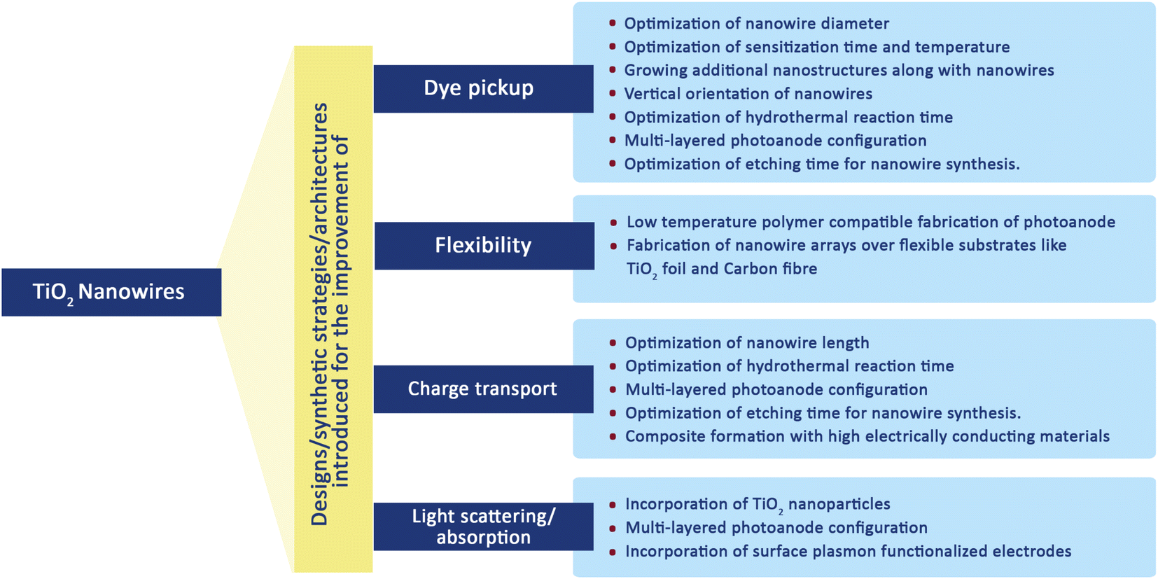 | ||
| Scheme 1 Various modifications introduced for the improvement of TiO2 nanowire based DSSC performance. | ||
Feng et al. presented a straightforward low-temperature method to fabricate single-crystalline rutile TiO2 nanowires through a nonpolar solvent/hydrophilic solid substrate interfacial reaction under hydrothermal conditions.75 Nanowires having lengths up to 5 µm can be grown vertically from the TCO glass substrate along the preferred direction by this approach. This arrangement has given an efficiency of 5.02% under AM1.5 irradiation by employing N719 dye on 2–3 µm long TiO2 nanowire arrays. An added advantage of this technique is the low temperature employed, which favours the use of polymers for cell fabrication. Thus, low-temperature methods of photoanode fabrication are found to be compatible with polymer substrates and can result in flexibility. As part of developing flexible and lightweight DSSCs, Liao et al. introduced hierarchial TiO2 nanowire (HNW) arrays grown on a Ti foil substrate instead of FTO.125 These HNW arrays contain long TiO2 nanowire trunks and short TiO2 nanorod branches and are prepared by a two-step hydrothermal process. Liao et al. are the first to report such HNW arrays fabricated on Ti foil and they also replaced the Pt counter electrode with another electrode in which PEDOT is electrodeposited on the ITO-PET substrate. Even though HNW array DSSCs showed increased efficiency (4.32%) compared to that of NW-based DSSCs, the former possesses a comparatively reduced electron lifetime and transport time. As a further step toward realising lightweight and flexible DSSCs, cells were constructed with a vertical TiO2 nanowire array grown in situ on carbon fibre substrates as shown in Fig. 7.126
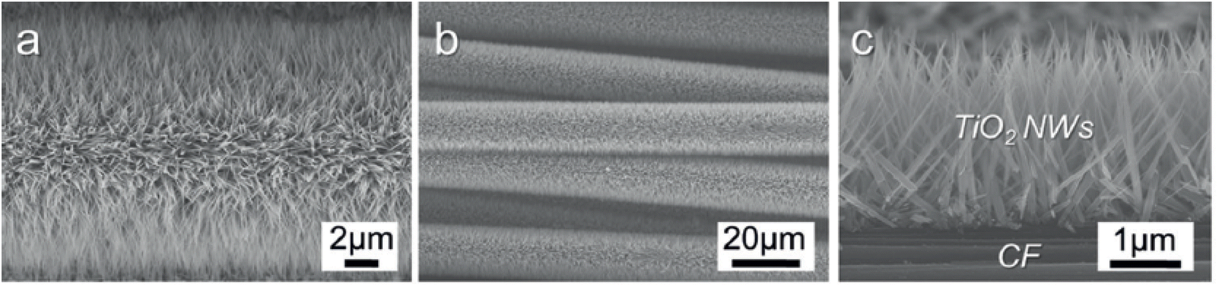 | ||
| Fig. 7 (a–c) Field emission (FE)-SEM images of TNW arrays grown on a CF substrate at 190 °C for 80 min.126 (Reprinted with permission from ref. Cai et al., 2014. Copyright 2014 WILEY-VCH Verlag GmbH & Co. KGaA, Weinheim.) | ||
In 2015, Liu et al. reported the controllable formation of TiO2 nanowire arrays on a titanium mesh. This method is a hydrothermal one capable of forming nanowire arrays (NWAs) with an average diameter of 80 nm.127 Along with studying the influence of NWA preparation conditions on DSSC parameters, Liu et al. also focused on the role of the sensitization temperature and time on DSSC performance.127 They found that a higher sensitization temperature would benefit dye molecule infiltration to the internal areas of NWA films, and the complete covering of monolayer dye molecules on the surface of TiO2 NWAs would enhance the photovoltaic properties of the DSSC. By maintaining optimum conditions, Liu et al. obtained an efficiency of 3.42% for a flexible DSSC. Apart from maintaining optimum dye pickup, they were found to have depressed charge recombination also. Later several groups tried enhancing the available surface area of the photoanode by growing additional structures on TiO2 nanowires. In 2014, single-crystal-like 3D TiO2 branched nanowire arrays were fabricated by Sheng et al. with the 1D branch epitaxially grown from the primary trunk.128 This attempt made by Sheng et al. increased the available surface area by 71% and they also exhibited a fast charge transport property compared to one-dimensional TiO2 nanowires. Sheng obtained an efficiency of 4.61% for branched nanowire-based DSSCs.128 It is found that the presence of other nanostructures as branches on nanowires creates additional boundaries in electron transport. Later, DSSCs with multilayered photoanodes, in which different functions were assigned to specific layers, were fabricated. For example, in 2013, Bakshayesh et al. introduced a new TiO2 structure with corn-like nanowire morphology having high surface area and crystallinity synthesised by the surface tension stress mechanism.129 They have adopted a double-layer DSSC design consisting of an underlayer of anatase TiO2 nanoparticles and an overlayer of corn-like TiO2 nanowires as shown in Fig. 8a and Fig. 8b shows the photocurrent against voltage curves. By adopting a triple function mechanism with effective management of light scattering, dye sensitization and photogeneration of charge carriers, Bakshayesh et al. attained an efficiency of 7.11%. Here the increased surface area of corn-like nanowires resulted in improved dye sensitization and short circuit current density. At the same time, the presence of NPs on corn-like nanowires increased light scattering. Most of the multilayer photoanodes follow such division of labour among various layers. Another new morphology reported in 2013 consists of thornbush like TiO2 nanowires (TBWs) prepared by a facile single-step hydrothermal method using potassium titanium oxide oxalate dehydrate, diethylene glycol (DEG) and water at 200 °C.130 These TBWs consist of a large number of nanoplates and nanorods. Depending on the change in the DEG/water composition, the diameter, as well as the morphology of TBWs, varies. TBWs having a diameter of 200 nm shows higher efficiency (5.2%) than those having a diameter of 400 nm (4.5%) and 600 nm (3.4%). Further treatment of TBW200 with graft-copolymer-directed, organized mesoporous TiO2 helps to increase the surface area and interconnectivity of TBWs leading to an enhanced efficiency of 6.7%. As the electron transport in TiO2 nanowires depends on their length, efforts were made to modify the nanowire length. In 2011, a multicycle hydrothermal synthetic process to produce vertically oriented, single-crystalline rutile TiO2 nanowires with lengths in between 1 and 8 µm was reported by Zhou and co-workers.131 It is observed that a further increase in the nanowire length does not give an expected increase in efficiency. This can be attributed to a decrease in surface area by fusion and widening at the base of nanowires.
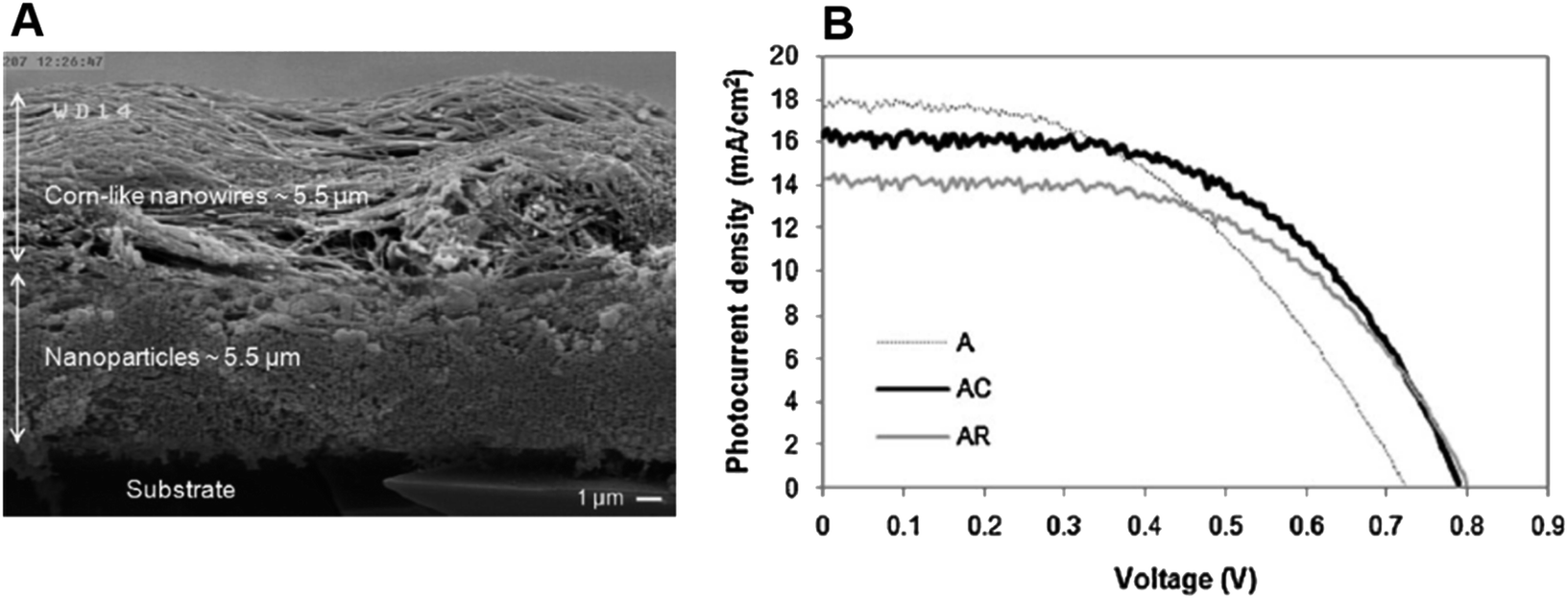 | ||
| Fig. 8 (a) FE-SEM image of the cross sectional view of a double-layer film containing TiO2 nanoparticles as the under-layer and corn-like TiO2 nanowires as the over-layer. (b) Photocurrent density–voltage curves of fabricated TiO2 solar cells [A-TiO2 NP solar cell, AC- Corn like TiO2 NW solar cell, AR-Regular TiO2 NW solar cell].129 (Reprinted with permission from ref. Bakhshayesh, A. et al., 2013. Copyright 2012 Elsevier Ltd.) | ||
In the same year, a double-sided brush-shaped (DSBS) TiO2 nano architecture consisting of highly ordered TiO2 nanowires aligned around an annealed TiO2 nanoparticle layer was prepared by C. Zha and team via the hydrothermal method.132 Here nanowire growth is seeded by the annealed nanoparticle layer and it supports the DSBS structure. It was found that by varying the hydrothermal reaction time, structural properties like the crystalline phase, phase composition, length of the nanowires and thickness of the nanoparticle layer can be tuned. They have obtained an efficiency of 5.61% from an 8 hour reaction time and nanowires of length 6 µm. Thus, the microstructure has a significant influence on solar cell performance and the DSBS structure is a greatly promising one. Later Qiang Wu and co-workers fabricated a DSSC based on a self-assembled, vertically aligned TiO2 nanowire photoelectrode sensitized with N719 (ref. 133) sensitizer and it could achieve an efficiency of 9.40% (Fig. 9).134 Here TiO2 nanowires on an FTO glass plate have a tuneable length in the range of 15–55 µm and are suitable for multi-layered photoanode configuration.134 The same team of Wu et al. reported another distinct and novel architecture with the integration of various three-dimensional, hyperbranched titania nanoarchitectures into a multi-stack. The multi-stacked layers consist of an underlayer of hyperbranched hierarchical tree-like titania nanowires, branched hierarchical rambutan-like titania hollow submicrometer-sized spheres as the intermediate layer and hyperbranched hierarchical urchin-like titania micrometre-sized spheres as the top layer.135 Here the bottom layer enhances electron transport through one-dimensional nanowires into the FTO plate whereas the middle layer can guarantee effective light-trapping efficiency through the hollow-hole structure of submicrometer-sized macroporous TiO2 spheres and the upper layer of hyperbranched hierarchical TiO2 microspheres can offer increased light scattering ability. This integrated photoanode achieved an efficiency of 11.01% which is far better compared to that of its TiO2 NP analogue.
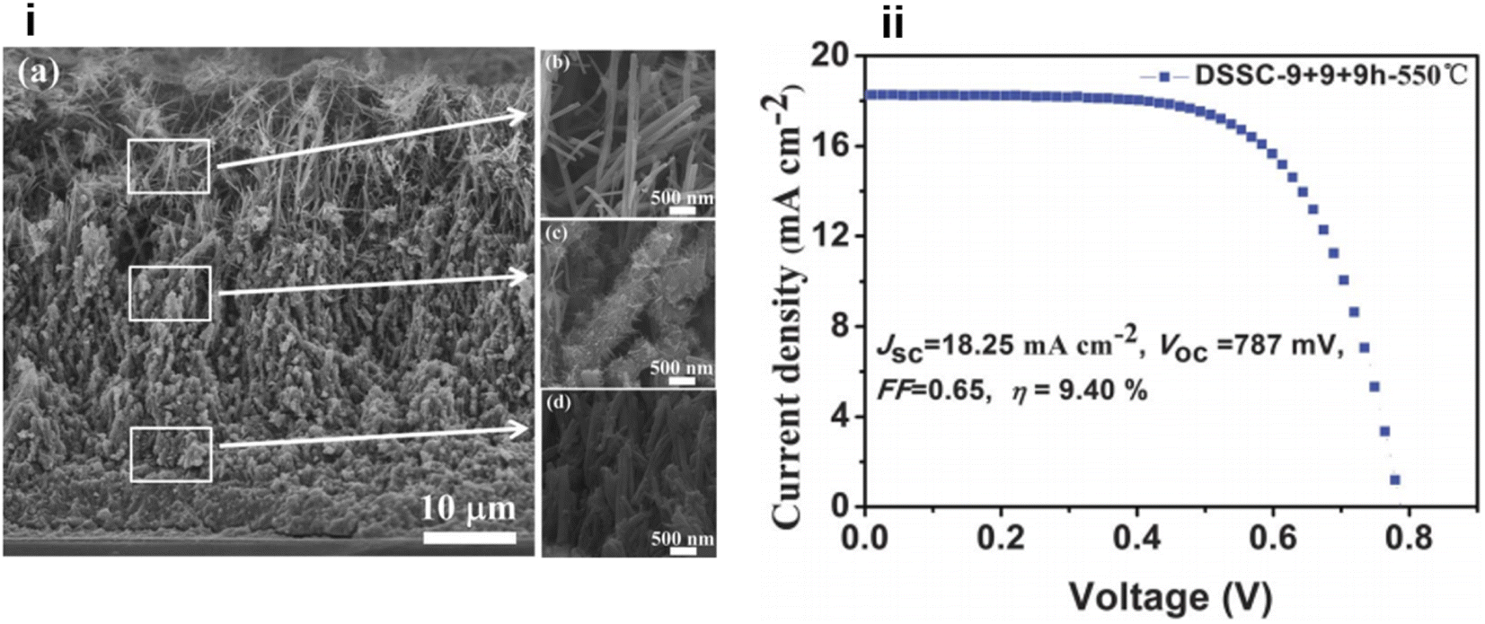 | ||
| Fig. 9 (i) (a) The cross-sectional SEM images of MTNWs on FTO glass prepared after three hydrothermal cycles (9 + 9 + 9 h); (b, c, and d) the FE-SEM images of the upper, intermediate and bottom layers of the as prepared MTNWs, respectively. (ii) J–V characteristic of DSSCs based on the 47 mm thick TiO2 NWs prepared with 3 hydrothermal cycles and followed by 550 °C calcination treatment.134 (Reprinted with permission from ref. Wu et al., 2014. Copyright 2013 Royal Society of Chemistry.) | ||
In 2016, Hailiang Li et al. constructed vertically aligned rutile TiO2 nanowire arrays (NWAs) with a length of ∼44 µm on transparent conductive fluorine-doped tin oxide (FTO) glass by a facile one-step solvothermal method without using any surfactant or template.136 By controlling the ethanol content in the reaction mixture, the length and separation between the NWs can be controlled. A reaction mixture containing 20 mL ethanol facilitated the formation of TiO2 NWAs with an efficiency of 8.9%. This can be further enhanced to 9.6–10.2% by incorporating a light scattering layer into the TiO2 NWA-based DSSC.
Another mode of enhancement of light absorption and efficiency of DSSCs utilizes the anti-reflecting (AR) property of photoanode materials. Another approach is by the exploitation of the surface plasmonic effect of metal nanoparticles. Yen et al. fabricated a DSSC utilizing both the antireflecting character and plasmonic effect. Their DSSC was equipped with a 3D TNW-AuNP plasmonic electrode having antireflective (AR) TiO2 nanowires (TNWs) serving as light-harvesting antennae coupled with Au nanoparticles (NPs).137 These plasmonic functionalized electrodes (PFEs) exhibited a remarkable plasmonic red shift from 520 nm to 575 nm. Such PFEs were developed to overcome the narrow absorption range and low absorption coefficient of dyes. It was found that TiCl4 treatment can increase the efficiency of TNW-AuNP hybrid DSSCs from 6.25% to 9.73%. In the same year, Lee et al. investigated the photovoltaic performances of back-illuminated DSSCs employing TiO2 NP/NW composite films of various weight percentages.138 These DSSCs used a cobalt-based electrolyte system. In NP/NW composite films NPs help to increase the surface area whereas NWs facilitate efficient charge transfer. The highest efficiency of 7.37% was shown by DSSCs with 10 wt% of NWs in the NP/NW composite film which is 20% improved compared to that of a pure NP-based DSSC. Apart from the widely used hydrothermal method of nanowire synthesis, Jin et al. proposed an approach for fabricating TiO2 nanowire networks on Ti foil using a Ti corrosion reaction in KOH aqueous solutions at different temperatures, followed by a further ion-exchange process.139 These photoanodes were suitable for bendable DSSCs and have exhibited an efficiency of 1.11% for back illumination. The same team also tried growing TiO2 nanowire networks on FTO substrates by wet corrosion and obtained an efficiency of 1.0% under AM 1.5 illumination.140 In 2017 Li and co-workers reported a simple single-step hydrothermal method to prepare single-crystalline self-branched anatase TiO2 NWs by using TBAH and CTAB as co-surfactants.141 These single crystalline self-branched TiO2 NW-based DSSCs exhibited an efficiency of 6.37% which is due to an enhanced percentage of exposed (010) facets having high dye adsorption capacity. Again in 2018, another design was introduced into the class of FDSSCs (fiber shaped dye-sensitized solar cells) which consists of a stretchable spring-like Ti@TiO2 nanowire array as the photoanode by Liu and co-workers. This design was intended to achieve higher flexibility and elasticity of DSSCs and the spring-like Ti@TiO2 array was prepared by the hydrothermal technique at a controlled NaOH concentration. Liu's team was the first to achieve a 100% stretching degree in FDSSCs with a PCE retention rate of 95.95% upon bending accompanied by 100% stretching strain.142 Another major finding was made by Ni et al., that the enhanced surface area of nanowire arrays achieved on prolonged etching treatment can improve the dye intake but it reduces the PCE by increased electron recombination. Even then, Ni and co-workers succeeded in attaining an improved PCE of 9.39% by employing an additional scattering layer of TiO2 particles along with rough surface rutile TiO2 nanowire arrays.143 Thus, light scattering layers can make up for the loss encountered by extended rates of photo electron recombination. As a way of minimising charge recombination and improving electron transport across TiO2 nanowires, developing composites with materials having high electrical conductivity and charge carrier mobility was found exciting. One such approach was carried out by Makal and Das in 2021 by fabricating a reduced graphene oxide laminated one-dimensional TiO2–B nanowire composite based photoanode.144 The effect of different reduced graphene oxide loadings on the PCE of the DSSCs was evaluated and it was found that an 8 wt% loading showed a PCE of 4.95%. Makal and Das used the same design to develop another photoanode material where they encapsulated TiO2–B nanowires with graphitic carbon nitride (g-C3N4) and the PCE for the developed cell was found to be 5.12%.145 This is one of the highest efficiencies reported for a DSSC with a TiO2–B based photoanode. Significant efforts carried out for increasing the performance of nanowire-based DSSCs are discussed above and are tabulated in Table 1.
| DSSC Type | Author | Photoelectrode and method of preparation | Sensitizer | Electrolyte | Efficiency | Ref. |
|---|---|---|---|---|---|---|
| DSSC with TiO2 nanowire arrays | Feng et al. | Vertically aligned single-crystalline TiO2 nanowire arrays by nonpolar solvent/hydrophilic solid substrate interfacial reaction under hydrothermal conditions | N719 | MPN-100 (Solaronix, Inc., Switzerland) containing tri-iodide in methoxypropionitrile | 5.02% | 75 |
| DSSC with hierarchical TiO2 nanowires (HNW) | Liao et al. | Hierarchical TiO2 nanowire (HNW) arrays grown on a Ti foil substrate instead of FTO by a two step hydrothermal process | N719 | I−/I3− based liquid electrolyte, which contained 1-methyl-3-propylimidazolium iodide (PMII), guanidinium thiocyanate and tert-butylpyridine in acetonitrile and valeronitrile | 4.32% | 125 |
| DSSC with a TiO2 nanowire array grown in situ on carbon fibre | Cai et al. | Vertically aligned TNW arrays in situ grown on carbon fiber (CF) substrates through a facile, controllable, and seed-assisted thermal process | N719 | I2, 1,3-dimethylimidazolium iodide, 4-tert-butylpyridine, guanidine thiocyanate, and LiClO4 in acetonitrile | 4.18% | 126 |
| DSSC with TiO2 nanowire arrays on a titanium mesh | Liu et al. | Controllable formation of TiO2 nanowire arrays with average diameter 80 nm on a titanium mesh by a hydrothermal method | N719 | I2, 1,3-dimethylimidazolium iodide, 4-tert-butylpyridine, guanidine thiocyanate, and LiClO4 in acetonitrile | 3.42% | 127 |
| DSSC with 3D TiO2 branched nanowire arrays | Sheng et al. | Single-crystal-like 3D TiO2 branched nanowire arrays consisting of a 1D branch epitaxially grown from the primary trunk prepared by a solvothermal method followed by exposure to O2 plasma | N719 | 1-Hexyl-2,3-dimethylimidazolium iodide and iodine in methoxypropionitrile | 4.61% | 128 |
| DSSC with TiO2 nanowires and TiO2 NPs | Bakshayesh et al. | Double layered photoanode having corn like TiO2 nanowires prepared by a surface tension stress mechanism | N719 | Dimethylpropylimidazolium iodide, LiI, I2, and 4-tert-butylpyridine in acetonitrile | 7.11% | 129 |
| DSSC with thornbush like TiO2 nanowires (TBWs) | Roh et al. | Thornbush like TiO2 nanowires (TBWs) prepared by a facile single step hydrothermal method | N719 | Dimethylpropylimidazolium iodide, LiI, I2, and 4-tert-butylpyridine in acetonitrile | 6.7% | 130 |
| DSSC with TiO2 nanowire array films | Zhou et al. | Vertically oriented, single crystalline rutile TiO2 nanowires by a multicycle hydrothermal synthetic process | N719 | LiI, I2, 1,2-dimethyl-3-n-propylimidazolium iodide (DMPII), and tert-butylpyridine in dehydrated acetonitrile | 2.0% | 131 |
| DSSC with TiO2 nanowires and TiO2 NPs | Zha et al. | Double sided brush shaped (DSBS) TiO2 nano architecture consisting of highly ordered TiO2 nanowires aligned around an annealed TiO2 nanoparticle layer was prepared by a hydrothermal method | N719 | 1-Butyl-3-methyl imidazolium iodide, I2, guanidinium thiocyanate, and 4-tert-butylpyridine in a mixture of acetonitrile and valeronitrile | 5.61% | 132 |
| DSSC with TiO2 nanowire | Wu et al. | Vertically aligned anatase TiO2 nanowires on FTO glass with a tunable length in the range of 15–55 mm for multilayered configuration of the photoanode by a hydrothermal method | N719 | I−/I3− redox electrolyte | 9.40% | 134 |
| DSSC with multistacked three dimensional, hyperbranched titania nanoarchitectures | Wu et al. | Photoelectrode with multistacked layers having integrated functions | N719 | 1-Methyl-3-propylimidazolium iodide (PMII), LiI guanidinium thiocyanate, I2, and tert-butylpyridine in acetonitrile and valeronitrile | 11.01% | 135 |
| DSSC with TiO2 nanowires | Jiang et al. | TiO2 nanowire array electrodes are prepared by a hydrothermal method followed by silanization | N719 | Ferrocene (Fc), ferrocenium tetrafluoroborate (Fc+), and tetrabutylammonium tetrafluoroborate | 0.749% | 146 |
| DSSC with TiO2 nanowires | Li, H. et al. | Vertically aligned rutile TiO2 nanowire arrays (NWAs) by a single step solvothermal method without using any surfactant or template | C106 | DMII, LiI, I2, TBP, and GNCS in the mixture of acetonitrile and valeronitrile | 8.9% | 136 |
| DSSC with a TNW-AuNP hybrid structure | Yen et al. | 3D TNW-AuNP plasmonic electrode prepared by hydrothermal and sputtering techniques | N719 | I2, LiI, DMPII, and TBP in acetonitrile | 9.73% | 137 |
| DSSC with NP/NW composite films | Lee et al. | TiO2 nanoparticle (NP)/nanowire (NW) composite films with various compositions are prepared by a solvothermal method | MK-2 dye | Cobalt redox couple | 7.37% | 138 |
| DSSC with a TiO2 nanowire network | Jin et al. | TiO2 nanowire networks on Ti foil using a Ti corrosion reaction | N719 | Iodolyte AN-50, Solaronix, Aubonne, Switzerland | 1.11% | 139 |
| DSSC with TiO2 nanowire networks | Shin et al. | TiO2 nanowire networks on FTO substrates by wet corrosion | N719 | Iodolyte AN-50, Solaronix | 1.0% | 140 |
| DSSC with TiO2 nanowires | Li et al. | Single crystalline self-branched anatase TiO2 NWs by a hydrothermal method using TBAH and CTAB as co-surfactants | N719 | LiI, I2, dimethylpropylimidazolium iodide (DMPImI) and tert-butylpyridine in a dry mixed solution | 6.37% | 141 |
| DSSC with a Ti@TiO2 nanowire array | Liu et al. | Spring like Ti@TiO2 nanowire array was prepared by a hydrothermal technique at a controlled NaOH concentration | N719 | 1,3-Dimethylimidazolium iodide I2, LiClO4, 4-tert-butylpyridine and guanidine thiocyanate in acetonitrile | 2.787% | 142 |
| DSSC with a rutile TiO2 nanowire array | Ni et al. | Rough surface rutile TiO2 nanowire array prepared by a hydrothermal method and prolonged etching. An additional light scattering layer of TiO2 particles was also employed | C109 | 1,3-Dimethylimidazolium, lithium iodide, iodine, tert-butylpyridine, and guanidinium thiocyanate in acetonitrile and valeronitrile | 9.39% | 143 |
| DSSC with reduced graphene encapsulated TiO2–B nanowire composite | Makal et al. | Reduced graphene oxide encapsulated TiO2–B nanowire composite synthesized by a hydrothermal method | N3 | Iodolyte AN-50 | 4.95% | 144 |
| DSSC with a g-C3N4 encapsulated TiO2–B nanowire composite | Makal et al. | g-C3N4 encapsulated TiO2–B nanowire composite synthesized by thermal calcination of hydrothermally grown TiO2–B nanowires and melamine | N3 | Iodolyte AN-50 | 5.12% | 145 |
3.2. Nanorods
Nanorods (NRs) are introduced into DSSC photoanode fabrication (Fig. 10) with the objective of increasing DSSC performance by exploiting their one-dimensional nanoscale properties. TiO2 nanorods facilitate easy electron transfer by utilising their specific geometry (Fig. 11) and reducing the ohmic loss during the electron transfer through the mesoporous titania layer.147 Various methods have been used for the synthesis of TiO2 nanorods for DSSC applications. Along with the introduction of novel synthesis strategies, efforts were made to modify the morphology and surface properties of TiO2 nanorods as given in Scheme 2.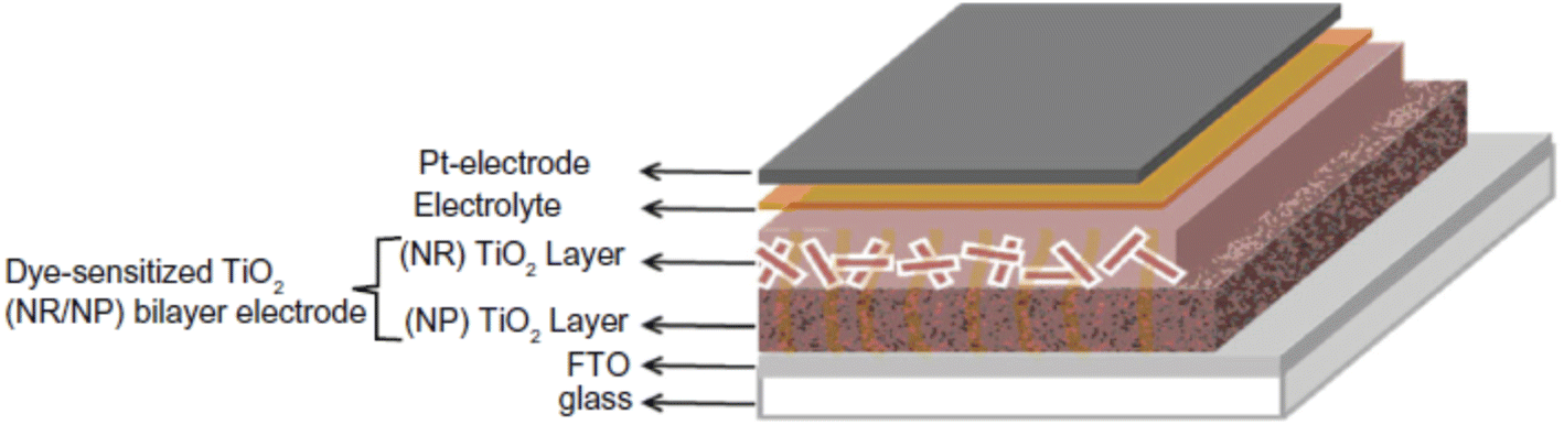 | ||
| Fig. 10 Schematic representation of the DSSC based on a TiO2 NR/NP bilayer photoanode.150 (Reprinted with permission from ref. Hafez et al., 2010. Copyright 2010 Hafez et al., publisher and licensee Dove Medical Press Ltd.) | ||
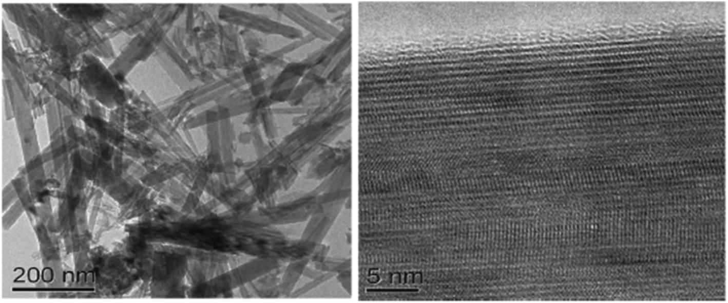 | ||
| Fig. 11 TEM images of the TiO2 nanorod sample and the HRTEM image of the nanorod.150 (Reprinted with permission from ref. Hafez et al., 2010. Copyright 2010 Hafez et al., publisher and licensee Dove Medical Press Ltd.) | ||
 | ||
| Scheme 2 Various modifications introduced for the improvement of the performance of TiO2 nanorod based DSSCs. | ||
A widely used fabrication method for TiO2 nanorods was the solvothermal method. Several studies on TiO2 nanorods were reported based on solvothermal techniques.147–160 Most of the solvothermal methods used for TiO2 nanorod fabrication employ water as a solvent i.e. the hydrothermal method. Sometimes the solvothermal method may be a multi-step process or a combination of more than one synthetic method. In 2005 Jiu et al. reported the synthesis of single crystalline anatase TiO2 nanorods by a surfactant-assisted hydrothermal method. These nanorods were found to exhibit an efficiency of 7.06%. Higher fill factor (FF) values of TiO2 NRs were observed compared to those of P25 nanoparticles, indicating the easier electron transport (lower resistance) through nanorods. In 2006, Jiu et. al. prepared single-crystalline anatase TiO2 nanorods by a surfactant-assisted hydrothermal method with control over the size and diameter. Here nanorods having a length of 100–300 nm and diameter of 20–30 nm were synthesized and they showed an efficiency of 7.29%.147 Jiu et al. achieved shape conservation and size regulation of nanorods with the help of a copolymer. Later Liu et al. found that the diameter, length and density of the nanorods prepared by the solvothermal method could be varied by changing the growth conditions such as growth time, growth temperature, initial reactant concentration, acidity and additives.161 Efforts of Liu et al. resulted in the formation of single-crystalline rutile TiO2 nanorods having an efficiency of 3%. In the very next year, a significant increase in conversion efficiency (7.9%) was achieved by De Marco et al. using TiO2 nanorods prepared by a single-step solvothermal technique.149 The obtained anatase TiO2 nanorod crystals were converted into screen printable paste for easy application into DSSCs. Here the solvothermal method helped to avoid coarse aggregation and shape loss of nanorods. Using the alkali hydrothermal technique, a novel morphology i.e. fan-shaped rectangular parallelepiped TiO2 rods were synthesized by Shao et al. with a conversion efficiency of 6% obtained for 1 M NaOH utilizing DSSCs and this efficiency is found to be 66.7% higher than that of P25-DSSCs.153,162 Investigations carried out at different NaOH concentrations showed that the morphology and crystal phase of the nanorods are affected by the alkali concentration. Kathirvel et al., Liu et al. and Zhang et al. reported the highest efficiencies for solvothermal derived TiO2 nanorods.158–160 Oriented rutile TiO2 nanorod arrays were grown in situ on an FTO (fluorine doped tin oxide) coated glass substrate by using a mixed acid medium composed of titanium tetraisopropoxide (TTIP), hydrochloric acid (HCl), acetic acid (AcOH) and water (H2O) as the solvent.152 An acid mixture with HCl:AcOH in a volume ratio of 4:8 produced oriented, uniform, thin rutile nanorods which were found to be superior to single acid-grown nanorods. They have shown an efficiency of 4.03% using 2.3 µm long nanorods. Zhang and co-workers introduced an oriented attachment mechanism for the fabrication of size and shape tuneable anatase TiO2 NRs.158 These single crystalline long TiO2 NRs have reduced grain boundaries which lead to enhanced charge collection. Thus, long thin NR-based DSSCs exhibited an efficiency of 8.87%. In 2015 Liu et al. prepared single-crystalline anatase TiO2 nanorods by a solvothermal method in which tetrabutylammonium hydroxide (TBAH) is used as the morphology controlling agent.159 DSSCs fabricated using these NRs have achieved an efficiency of 8.66%. Recently, several single and multi-step solvothermal fabrications of TiO2 NRs were reported.160,163–165 Later it is found that employing a composite structure of nanorods (NR) and nanoparticles (NP) in the photoanode can complement the advantages of each other. The first bilayer NR/NP composite structured photoanode was fabricated by Hafez et al.150 Here the sol–gel derived NP layer was coated with hydrothermally prepared NRs and this DSSC assembly exhibited an efficiency of 7.1%. Several NR/NP bilayered photoanode structures were fabricated later.151,155,156,166–170 These bilayer structures provided enhanced light scattering as well as increased surface area, which is finally reflected in their increased efficiencies (Fig. 12). The bilayer design proposed by Rui and co-workers enabled the synthesis of size tuneable rutile TiO2 nanorod microspheres by controlled hydrolysis during solvothermal synthesis and can be employed as a scattering over-layer in bilayer DSSCs.156 Rui et al. achieved an efficiency of 8.22% whereas the efficiency of the single layer reference cell was 7.00%. Better performance of the TiO2 NP/NR composite was obtained by Chatterjee and co-workers by employing a 1:1 wt% composite obtained from hydrothermally derived NRs and commercially available TiO2 powder.171 The obtained PCE of 8.61% was the highest among the photoanodes fabricated out of TiO2 NR/NP composites. Shao et al. introduced low-temperature fabrication of photoanodes for flexible DSSCs by electrophoretic deposition (EPD).167 The obtained NR/NP structures (NRPs) have high surface charges and wide size distribution. In addition, a multiple EPD process was adopted to form a better quality microstructured photoanode. In the same total time, the efficiencies of the multiple devices are more than 2.2 times that of one-step devices. Without any calcination or compression, the best device fabricated with multiple EPD and a thin layer of nanoparticles gives a conversion efficiency of 4.35%. Using a two-step hydrothermal method a novel bilayer structure composed of one-dimensional nanorods, which can serve as direct electron transport pathways and a three-dimensional hierarchical structure acting as a light scattering as well as large surface area layer for dye loading was introduced by Li et al.168 The dependence of the TiO2 NR/NP structured composite's photoanode efficiency on the amount of NRs was studied by researchers and it was found that efficiency is the maximum for composites having 10% NR content (4.89%).172 Another method employed for nanorod synthesis was electrospinning. Fujihara et al. employed electrospun TiO2 nanofibres as precursors for nanorods and these rods were spray dried onto an FTO plate.173 These spray deposited nanorods overcame the adhesion difficulties of nanofibres and exhibited an efficiency of 5.8%. Another electrospun synthesis was done by Jose et al. and they yielded 5.1% efficiency.190 In 2009 DSSCs having an efficiency of 9.52% were fabricated by Lee et al. using a combination of sol-gel and electrospinning techniques. Here nanorods were electrospun from a solution of titanium n-propoxide and polyvinyl acetate in dimethyl formamide.174 They have conducted a comparative study of nanorod and nanoparticle based DSSCs. These studies revealed that nanorod DSSCs have a pore volume double that of nanoparticle cells. Obviously the surface area available for sensitizers in nanorods is ∼2.5 times that of the nanoparticle based DSSC at equal TiO2 weights. Also, the electron–hole recombination time for nanorods is found to be more than eight times that of nanoparticle DSSCs. Later in 2013 MWCNTs were introduced as electron transporting superhighways into TiO2 nanorods by the electrospinning technique (Fig. 13). This incorporation was done by Yang et al. and they obtained an efficiency of 10.24%.175 In the same year Chen et al. employed a microemulsion electrospinning technique to synthesize TiO2 nanorods as a composite of mesopores and macropores by using paraffin oil droplets as the template.166 This microemulsion electrospinning approach achieved 8.53% efficiency for bilayer DSSC architecture with NRs as the scattering layer.
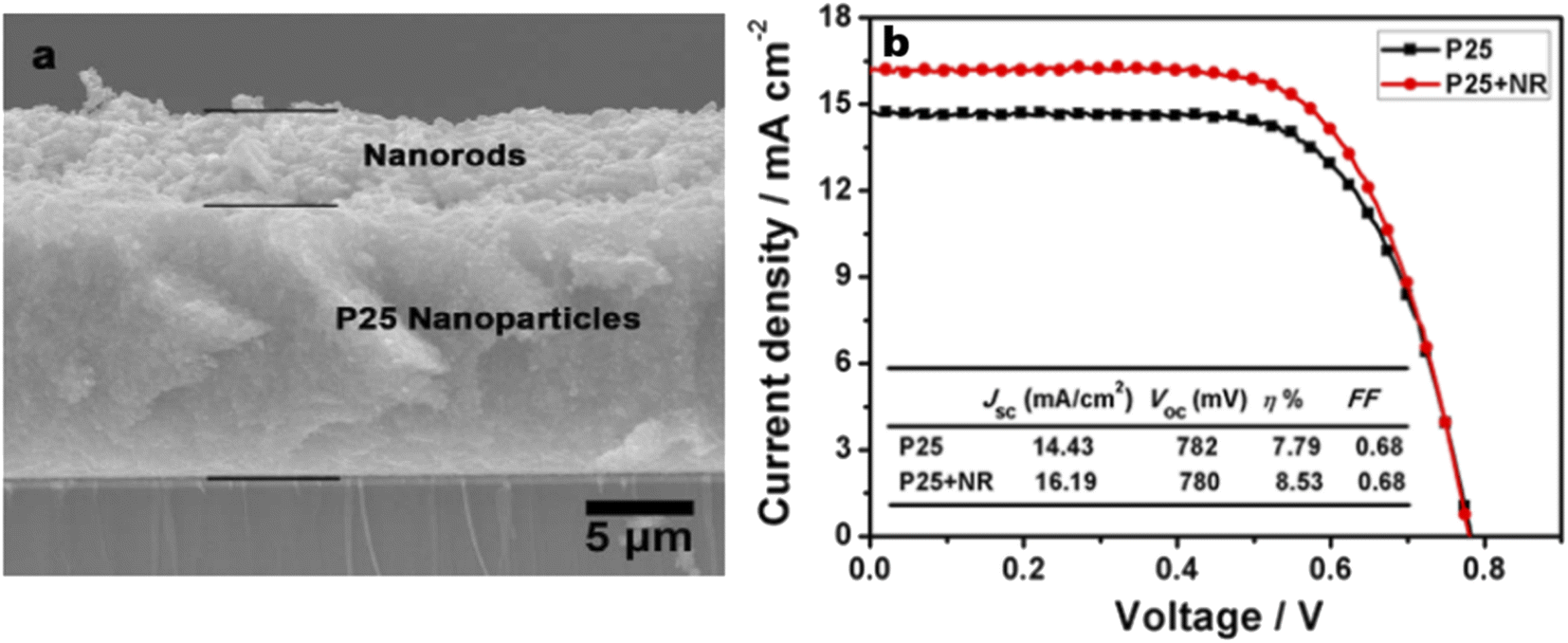 | ||
| Fig. 12 (a) Cross section SEM image of the bi-layer structured photoanode with a P25 nanoparticle bottom layer and porous nanorod top layer; (b) comparison between J–V curves of cells based on the bi-layer photoanode and single-layer P25 photoanode with the same thickness.166 (Reprinted with permission from ref. Chen, H.-Y. et al., 2013.Copyright 2013 American Chemical Society.) | ||
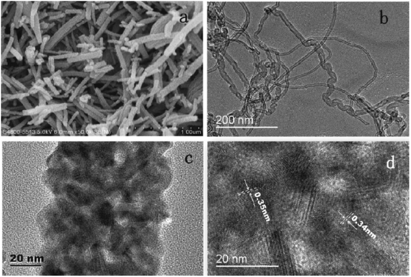 | ||
| Fig. 13 SEM and TEM images: (a) SEM image of TiO2 nanorods incorporating MWCNTs; (b) and (c) are TEM images, respectively, of MWCNTs and TiO2 nanorods incorporating MWCNTs; (d) HRTEM image of TiO2 nanorods that incorporate MWCNTs.175 (Reprinted with permission from ref. Yang and Leung, 2013.Copyright 2013 WILEY‐VCH Verlag GmbH & Co. KGaA, Weinheim.) | ||
In 2011 it has been reported that nanorods prepared by the hydrothermal method were used as seeds for the synthesis of a TiO2 nano-branched photoanode.176 This nano-branched array has achieved an efficiency of 3.75%.
Efforts were made to make NR-based DSSCs flexible by growing NRs on substrates other than the FTO plate. Such an innovative electrode architecture was introduced by Guo and their team, in which bunched TiO2 nanorods were grown on carbon fibres by a ‘dissolve and grow’ method.177 By using these carbon fibres coated with bunched TiO2 nanorods, tube-shaped flexible 3D DSSCs have been prepared with an efficiency of 1.28%. Wang et al. made a similar attempt for enhancing flexibility by preparing single crystal nanorod assembled TiO2 cloth from carbon cloth templates. Wang et al. employed a rapid microwave heating process for TiO2 cloth synthesis and this DSSC assembly yielded an efficiency of 2.21%. Wang et al. investigated the influence of sensitizers such as N719, C218 and D205 on TiO2 nanorod array-based photoanodes and found out that the best efficiency is obtained from C218.178
Also, the performance of TiO2 NR array DSSCs depends strongly on the annealing temperature.179,180 Researchers found that annealed nanorod arrays show an improvement of more than 400% in efficiency compared to unannealed NRs. This increase can be attributed to reduced recombination and better electric contact between the NRs and FTO substrate. Efficiency improvement of TiO2 nanorod-based DSSCs can be made by surface modifications such as nanoparticle decoration,181 chemical etching,182 doping,183 TiCl4 treatment184etc. Ghaffari et al. showed that the generation of photoelectrons by Au NPs can help electron–hole separation and thereby result in enhanced fill factor (FF) and short circuit current values (Jsc).181 The photochemical reduction process under ultraviolet radiation was employed for loading Au NPs on TiO2 NRs. Yao et al. prepared Nd doped TiO2 NRs by the solvothermal method.183 Here the doped Nd ions enhanced the injection of excited electrons and thereby decreased the electron–hole recombination. The obtained efficiency was 4.4% which is 33.3% greater than that of the undoped analogue.
Later, a combination of TiO2 nanomorphologies with other nanomaterials gained considerable interest. One such photoanode material consists of an overlayer of TiO2 nanorods and an underlayer of TiO2 embedded ZnO nanoflowers.185 The double-layered design was introduced by Chen and co-workers and they achieved a photo conversion efficiency of 8.01%. A similar composite design consists of rutile TiO2 nanorods incorporated with an α alumina thin film.186 Here α alumina facilitated an enhanced electron lifetime and better charge transport. The α alumina incorporated TiO2 nanorod arrays exhibited a PCE of 6.5%.
To boost the charge collection efficiency of TiO2 nanorods, a layer of reduced graphene oxide (rGO) was wrapped over the nanorod surface by Subramaniam and his team.187 2 wt% rGO loaded nanocomposite was found to show a superior photo conversion efficiency of 4.54%. Another effort was made by Roy and co-workers to improve the electron transport which involved the wrapping of rutile TiO2 nanorod arrays with polyaniline (PANI) on their surface.188 Being a conducting polymer, PANI enhanced the electron transport and the conjugation helped to capture more photoelectrons which in turn diminished the recombination between photo excitons. The association of a TiO2 NR photoanode with PANI made more visible light absorption possible. Later Tang and co-workers reported that the higher the aspect ratios of TiO2 NRs, the higher the dye loading capacity and efficiency will be.189 Here NRs having different aspect ratios were prepared by controlling the reaction time. Also, improved performance of branched TiO2 NRs was investigated by Hu et al.164. Prominent research on TiO2 nanorod-based DSSC photoanodes is tabulated in Table 2.
| DSSC Type | Author | Photoelectrode and method of preparation | Sensitizer | Electrolyte | Efficiency | Ref. |
|---|---|---|---|---|---|---|
| DSSC with TiO2 nanorods | Jiu et al. | TiO2 single crystalline anatase nanorods prepared by a surfactant assisted hydrothermal method | N719 | LiI, 1,2-dimethyl-3-n-propylimidazolium iodide (DMPII), I2, and 4-tert-butylpyridine (TBP) in methoxyacetonitride | 7.06% | 148 |
| DSSC with TiO2 nanorods | Jiu et al. | Highly crystalline TiO2 nanorods synthesized by a hydrothermal process in a cetyltrimethylammonium bromide surfactant solution | N719 | LiI, 1,2-dimethyl-3-n-propylimidazolium iodide (DMPII), I2, and 4-tert-butylpyridine (TBP) in methoxyacetonitride | 7.29% | 147 |
| DSSC with TiO2 nanorods | Yao et al. | Monodispersed Nd-doped TiO2 nanorods were synthesized by solvothermal methods | N719 | LiI, I2, and 4-tert-butylpyridine in 3-methoxypropionitrile | 4.4% | 183 |
| DSSC with TiO2 nanorods | Fujihara et al. | TiO2 nanorods were obtained by mechanical grinding of electrospun TiO2 nanofibers | N3 Solaronix | Acetonitrile containing lithium iodide, iodine, 4-tert-butylpyridine and 1-propyl-2,3-dimethyl imidazolium iodide | 5.8% | 173 |
| DSSC with TiO2 nanorods | Jose et al. | TiO2 nanorods by electrospinning | D131, D102, D149 & N3 | Acetonitrile containing lithium iodide, iodine, 4-tert-butylpyridine, and 1-propyl-2,3-dimethyl imidazolium iodide | 5.1% | 190 |
| DSSC with TiO2 nanorods | Kang et al. | TiO2 nanorods prepared by an oriented attachment approach | N719 | 1-Methyl-3-propylimidazolium iodide (MPII), LiI, I2, and tert-butyl pyridine (TBP) in methoxypropionitrile (MPN) | 6.2% | 191 |
| DSSC with TiO2 nanorods | Lee et al. | TiO2 nanorod based photoelectrodes prepared by a combination of sol–gel chemistry and electrospinning | N719 | 1-Butyl-3-methylimidazolium iodide, iodine, guanidinium thiocyanate, and 4-tert-butylpyridine in acetonitrile/valeronitrile | 9.52% | 174 |
| DSSC with TiO2 nanorods | Liu et al. | Oriented single-crystalline rutile TiO2 nanorod films prepared by a hydrothermal method | N719 | 1-Butyl-3-methylimidazolium iodide, I2, tert-butylpyridine, and guanidinium thiocyanate in acetonitrile/valeronitrile | 3.0% | 161 |
| DSSC with TiO2 nanorods | De Marco et al. | TiO2 anatase nanorods prepared by a simple one-step solvothermal method | N719 | LiI, I2, 1-methyl-3-propylimidazolium iodide, and tert-butylpyridine in dried acetonitrile | 7.9% | 149 |
| DSSC with TiO2 nanorods | Hafez et al. | TiO2 nanorod/nanoparticle (NR/NP) bilayer electrode prepared by a hydrothermal method | N719 | Tetrapropylammonium iodide, iodine, lithium iodide, and 4-tert-butylpyridine in acetonitrile | 7.1% | 150 |
| DSSC with a TiO2 NP/NR composite | Saji et al. | TiO2 NPs and NRs were prepared by a surfactant-assisted thermal method | N3 | LiI, I2, and tert-butyl pyridine in 3-methoxy propionitrile | 4.89% | 172 |
| DSSC with TiO2 NRs/NPs | Fan et al. | Anatase TiO2 fusiform nanorod/NP photoanode prepared by a two step hydrothermal process | N719 | LiI, I2 and 4-tert-butylpyridine in 1:1 acetonitrile propylene carbonate |
4.68% | 151 |
| DSSC with TiO2 NRs/NPs | Huang et al. | Rutile TiO2 nanorod-array films grown from a mixed acid medium by a hydrothermal reaction | (2-Cyano-3-{5′-[1-cyano-2-(1,1,6,6-tetramethyl-10-oxo-2,3,5,6-tetrahydro-1H,4H,10H-11-oxa-3a-aza-benzo-[de]anthracen-9-yl)-vinyl]-[2,2′]bithiophenyl-5-yl}-acrylic acid | LiI, I2, DMPImI, and TBP using dehydrated AN as the solvent | 4.03% | 152 |
| DSSC with TiO2 NRs/NPs | Chatterjee et al. | 1:1 TiO2 NR-NP composites prepared by a hydrothermal technique with a hydrogen titanate nanorod precursor |
N719 | LiI, I2 and 4-t-butylpyridine in acetonitrile | 8.61% | 171 |
| DSSC with TiO2 nanorod arrays | Shao et al. | Fan-shaped rectangular parallelepiped TiO2 rods were prepared by an alkali hydrothermal method | N719 | LiI, I2, and tert-butylpyridine in acetonitrile | 6.0% | 153 |
| DSSC with branched rutile TiO2 nanorod arrays | Wang et al. | Rutile TiO2 nano-branched arrays grown directly on transparent conductive glass (FTO) by a facile two-step wet chemical synthesis process | N719 | 1,2-Dimethyl-3-propylimidazolium iodide, I2, guanidinium thiocyanate, and 4-tert-butylpyridine | 3.75% | 176 |
| DSSC with TiO2 nanorod arrays | Wang et al. | One dimensional TiO2 nanorod arrays prepared by a hydrothermal method | N719, C218 and D205 | 1-Propyl-3-methylimidiazolium iodide,I2, guanidinium thiocyanate, NaI, and N-methyl benzimidazole in 3-methoxypropionitrile | 1.51%(C218) | 178 |
| DSSC with TiO2 nanorod cloths | Wang et al. | Single-crystal nanorod assembled TiO2 cloth with carbon cloth as a template were prepared by a rapid microwave heating process | N719 | DMPII, LiI, I2 and 4-TBP in methoxypropionitrile | 2.21% | 192 |
| DSSC with TiO2 nanorods | Yang et al. | Single crystalline rutile nanorods grown on top of a fluorine doped tin oxide (FTO) substrate via a microwave assisted hydrothermal reaction | N719 | Iodolyte AN-50, (Solaronix) | 3.7% | 193 |
| DSSC with a Au NP deposited TiO2 nanorod array | Ghaffari et al. | Au nanoparticles were loaded onto the surface of hydrothermally prepared TiO2 nanorods via a photochemical reduction process | N719 | Guanidinium thiocyanate (GuSCN), I2, 4-tert-butylpyridine (TBP) and butylmethylimidazolium iodide (BMII) in a mixture of acetonitrile and valeronitrile | 0.94% | 181 |
| DSSC with a TiO2 nanorod array | Guo et al. | Rectangular bunched rutile TiO2 nanorod arrays grown on carbon fiber by an acid corrosion method | N719 | LiI, I2, and 4-tert-butylpyridine in 3-methoxypropionitrile | 1.28% | 177 |
| DSSC with TiO2 nanorods | Liu et al. | Anatase TiO2 nanorods were prepared by a facile two-phase hydrothermal method | N719 | LiI, I2, 1-methyl- 3-propylimidazolium iodide, and tert-butylpyridine in dried acetonitrile | 6.37% | 154 |
| DSSC with a spherical TiO2 nanorod-aggregate light-scattering layer | Liu et al. | Bilayer-structured photoelectrode film with spherical TiO2 nanorod aggregates as a light-scattering overlayer and nanocrystalline TiO2 as an underlayer prepared by a hydrothermal method | N719 | LiI, I2, 1,2-dimethyl-3-propylimidazolium iodide, and 4-tert-butylpyridine in acetonitrile | 6.1% | 155 |
| DSSC with TiO2 nanorods having a composite structure | Chen et al. | Ultraporous anatase TiO2 nanorods fabricated by a simple microemulsion electrospinning approach | N719 | I2, LiI, 1-methyl-3-propylimidazolium iodide (PMII), guanidinium thiocyanate, and tert butylpyridine in a mixture of acetonitrile/valeronitrile | 8.53% | 166 |
| DSSC with a spherical TiO2 nanorod-aggregate light-scattering layer | Rui et al. | TiO2 microspheres assembled by single crystalline rutile TiO2 nanorods were synthesized by one-pot solvothermal treatment | N719 | I2, LiI, 1-methyl-3-propylimidazolium iodide (PMII), guanidinium thiocyanate, and tert-butylpyridine in a mixture of acetonitrile/valeronitrile | 8.22% | 156 |
| DSSC with TiO2 nanorods and MWCNTs | Yang et al. | MWCNTs are introduced into TiO2 nanorods by electrospinning | N719 | I2, LiI, 1-methyl-3-propylimidazolium iodide (PMII) and 4-tert-butylpyridine in a mixture of acetonitrile/valeronitrile | 10.24% | 175 |
| DSSC with a TiO2 nanorod based network structure | Yu et al. | Three dimensional rutile-nanorod-based network structure was developed by a facile two-step hydrothermal process | N719 | Organic-based liquid electrolyte (HPE) that contained a I−/I3− redox couple was supplied by Dyesol (Australia) | 6.31% | 157 |
| DSSC with a TiO2 nanorod/nanoparticle (NRP) structure | Shao et al. | NRP structured photoanodes prepared by electrophoretic deposition (EPD) | N719 | LiI, I2 and tert-butylpyridine in acetonitrile | 4.35% | 167 |
| DSSC with TiO2 nanorods | Zhang et al. | Single crystal-like anatase TiO2 nanorods with a specific growth direction are prepared by a hydrothermal method | Z907 | 1,3-Dimethylimidazolium iodide, LiI, and I2 in a mixture of acetonitrile and valeronitrile | 8.87% | 158 |
| DSSC with a bilayered TiO2 photoanode | Li et al. | Bi-layer photoanode consisting of a hierarchical structure of one dimensional nanorods and three dimensional TiO2 was prepared by a hydrothermal method | N719 | LiI, I2, 1,2-dimethyl-3-propylimidazolium iodide (DMPII) and 4-tert-butylpyridine (4-TBP) | 5.61% | 168 |
| DSSC with TiO2 nanorods | Liu et al. | Single-crystalline anatase TiO2 nanorods were prepared by a solvothermal method | N719 | LiI, I2,dimethylpropylimidazolium iodide (DMPImI) and tert-butylpyridine in dry acetonitrile | 8.66% | 159 |
| DSSC with TiO2 nanorod arrays | Yuan et al. | Vertically ordered single-crystalline TiO2 nanorod arrays (NRAs) were prepared by a combination of hydrothermal and etching methods | N719 | LiI, I2, 1-propyl-3-methylimidazolium iodide and tert-butylpyridine in dry acetonitrile | 4.69% | 182 |
| DSSC with TiO2 nanorod arrays | Iraj et al. | Vertically aligned rutile TiO2 nanorod arrays were synthesized by a hydrothermal method | N719 | LiI, I2, 1-propyl-3-methylimidazolium iodide and tert-butylpyridine in dry acetonitrile | 1.86% | 165 |
| DSSC with TiO2 nanorods | Kathirvel et al. | Monodispersed TiO2 nanorods were prepared using a simple solvothermal process | N719 | Lithium iodide, iodine, 4-tert-butylpyridine and 1,2-dimethyl-3-propylimidazolium iodide was dissolved in acetonitrile | 9.21% | 160 |
| DSSC with TiO2 nanorods | Tang et al. | Single-crystalline anatase TiO2 nanorods with a high aspect ratio | N719 | LiI, I2, dimethylpropylimidazolium iodide (DMPImI) and tert-butylpyridine in a dry mixed solution | 7.51% | 189 |
| DSSC with TiO2 nanorods | Guli et al. | TiO2 nanorod arrays were synthesised through a facile one-step solvothermal route without any surfactant and template | N719 | 1.68% | 163 | |
| DSSC with branched hierarchical TiO2 nanorod arrays | Hu et al. | Rutile branched hierarchical TiO2 nanorod arrays were prepared by a facile two-step hydrothermal method | N719 | LiI, I2, 1-propyl-3-methylimidazolium iodide and tert-butylpyridine in dry acetonitrile | 2.01 | 164 |
| DSSC with TiO2/ZnO nanoflowers and TiO2 nanorod array | Chen et al. | Double layered photoanode having an overlayer of a TiO2 NR array and underlayer of a TiO2 embedded ZnO nanoflower array by a sol–gel method | N719 | LiI, I2 and LiClO4 in acetonitrile | 8.01% | 185 |
| DSSC with rutile TiO2 nanorods incorporated with α alumina | Sriharan et al. | Rutile TiO2 nanorods incorporated with α alumina were developed on an FTO surface via a hydrothermal route | N719 | KI, I2 and 4-tert-butyl pyridine | 6.5% | 186 |
| DSSC with a 3 dimensional hierarchical TiO2 nanorod array wrapped with rGO | Subramaniam et al. | Three dimensional hierarchial TiO2 nanorod arrays with a layer of rGO wrapping prepared by an in situ hydrothermal method | N719 | LiI/I2 in acetonitrile | 4.54% | 187 |
| DSSC with PANI wrapped rutile TiO2 nanorods | Roy et al. | Hydrothermal derived rutile TiO2 NRs wrapped with an in situ deposited layer of PANI | N719 | 1-Methylbenzimidazole (NMB) was mixed with a 1:1 volume ratio of acetonitrile and 3-methoxypropionitrile (MPN) solution followed by the addition of LiI, tetrabutylammonium iodide (TBAI), and I2 |
4.28% | 188 |
3.3. Nanotubes
TiO2 nanotubes were introduced with a hollow cavity structure, possessing a higher active surface area. Their enhanced absorption capacity and fast electron transport ability were examined by researchers194,195 and they were found suitable for DSSC applications as shown in Fig. 14. Gaps in TiO2 mesostructures, which act as electron traps, can be avoided by using nanotube arrays having small boundaries in between. This results in an increased diffusion length i.e. the distance travelled by an electron in a tube before recombination.196 It was estimated that the diffusion length of a nanotube cell is approximately 100 µm.197 So up to this limit, the tube size can be increased which in turn increases the surface area without promoting recombination. The oxidised species from the electrolyte can easily escape from nanotubes because of their ‘open’ structure as compared to from the mesoporous layers. Once it is oxidised, it will diffuse towards the cathode and get reduced back rapidly to minimise recombination losses.198 The drawbacks of TiO2 nanotubes are their high manufacturing cost and time-consuming preparation techniques.199 The efficiency of DSSCs employing TiO2 nanotubes is dictated by factors such as morphology and the crystalline structure of the tubes. It is observed that reduction in the tube diameter has a superior role in efficiency compared to the increase in the tube length.200 Also, dye loading depends on the annealing temperature of the nanotubes.200 The next factor is collection efficiency, which can be improved by minimising recombination losses by introducing modifications on the tube surfaces.201,202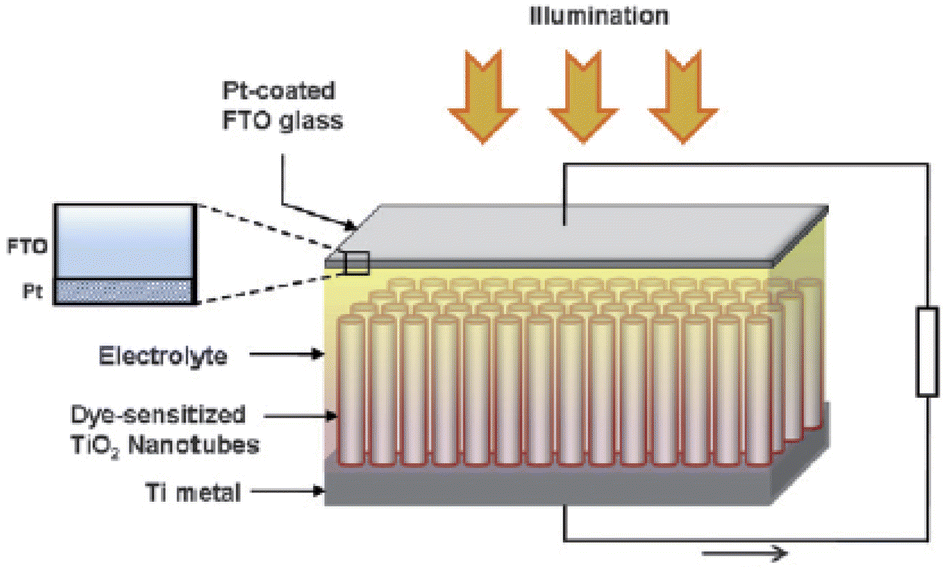 | ||
| Fig. 14 Schematic representation of typical solar cell construction using TiO2 nanotubes grown on a Ti substrate.76 (Reprinted with permission from ref. Roy et al., 2010. Copyright 2009, Royal Society of Chemistry.) | ||
Scheme 3 provides an overall idea of the efforts made to improve TiO2 nanotube based photoanode performance in DSSCs. Some of the significant nanotube-based DSSC architectures are discussed in this section. One of the earliest attempts involved the use of nanotube powders formed by a surfactant template-assisted technique.203 These disordered nanotube array has achieved an efficiency of 4.88%.203 The most widely employed technique for nanotube synthesis was electrochemical anodization.202–208 These electrochemical anodizations were carried out in different electrolytes by different research groups. Yi et al. investigated the influence of parameters like water content, anodization time and post-treatment of nanotubes on the photoconversion efficiency of the photoanodes.209 It is found that efficient systems can be developed out of a combination of anodization with other synthetic methods for the fabrication of hybrid and multi-layered photoanodes.210–216 Another simpler route of TiO2 nanotube synthesis proposed by Ramakrishnan and co-workers involved the hydrothermal treatment of quasi-crystalline TiO2 nanoparticles.217 They were reported to have achieved hydrothermal conditions even without using an autoclave. Apart from using individual nanotubes, designs involving nanotube arrays were made by certain research groups.194,204,206–208,210,212–215,218–220 For example, a highly ordered array of TiO2 nanotubes with a length of 360 nm was introduced in 2006 by Mor and co-workers with a PCE of 2.9%.221 This reduction in PCE is due to the comparatively smaller thickness of the photoelectrode. Mor et al. claimed that the efficiency can be further improved towards the ideal limit of ∼31% by increasing the length of the nanotube array up to a few micrometres. Wang et al. showed that efficiency can also be increased by treatment of TiO2 nanotube arrays with TiCl4 and ozone.202 Such a surface engineered TiO2 nanotube array attained an efficiency of 7.37%. Lei et al. brought the efficiency to 8.07%, employing one dimensional TiO2 nanotube arrays (Fig. 15a and b) prepared by anodization.206 The I–V plots obtained by Lei and team for the TNT/FTO film in comparison with the P25/FTO film are shown in Fig. 15c. Another report by Hun Park and co-workers shows that TiO2 nanotubes longer than 15 µm, transplanted on an FTO plate achieved an efficiency of 5.36% after TiCl4 treatment.207 TiO2 nanotube arrays were also subjected to doping with other elements.222–224 The intention of adding dopants is to perfectly match the LUMO of dye molecules to the conduction band of TiO2 for efficient electron transfer. This kind of perfect alignment will result in enhanced electron injection and reduced electron recombination. Yang et al. introduced TiO2 nanotubes doped with Nb by anodizing Ti–Nb alloys (η = 3.21%).222 Using the same technique, So et al. prepared Ru-doped TiO2 nanotubes from Ti–Ru alloys(η = 5.16%).223 While adding metal content it is found that the efficiency is the maximum for an optimum value of metal concentration. Also, metal doping will have an adverse effect if the length of the tubes is not correctly controlled. Subramanian et al. fabricated DSSCs with boron-doped TiO2 nanotube arrays.224 Here B doped nanotube arrays were prepared by anodization and they achieved an efficiency of 3.44% with an increased electron lifetime and reduced interface resistance. Besides doping, surface decoration with NPs and microspheres was also tried by different groups.205,208,210,214 Roy et al. observed that appropriate treatment of NTAs with TiCl4 will result in the decoration of the NTA surface with TiO2 nanocrystals.205 Such decorations enhanced dye pick up and thereby improved efficiency. He et al. decorated a TiO2 NTA with TiO2 microspheres synthesized by a microwave solvothermal process which yielded an efficiency of 7.24%.210Fig. 16 shows SEM images as well as I–V characteristics of He's photoelectrode. Rho et al. introduced open-ended free-standing TiO2 NTAs functionalized by Ag NPs and coated by TiO2 NPs.214 Here nanotube channels were functionalized with Ag NPs to create a plasmonic effect. At the same time, TiO2 NPs facilitate scattering. A combination of both these effects resulted in an efficiency of 7.05%. A similar plasmonic enhancement of power conversion efficiency was achieved with the incorporation of Au nanoparticles into TiO2 nanotube arrays by Chen et al.225 The obtained 19% improvement in PCE for the Au nanoparticle inlaid TNT arrays can be attributed to the surface plasmon resonance and scattering effect of the incorporated Au nanoparticles. In the same year, Guo and co-workers came up with a novel single-photon management architecture for a DSSC photoanode.226 Their design, consisting of a TiO2 nanotube photonic crystal deposited with Au nanoparticles, achieved a PCE of 5.63% which was the result of the synergistic effect of a photonic crystal and surface plasmon resonance of Au nanoparticles. Followed by this, in 2019, Fu et al. developed a cigar-like Au/TiO2 nanotube array/TiO2 nanoparticle multi-hierarchical photoanode with a PCE of 8.93%.227 The multi-hierarchical design, which was obtained via a novel vacuum-assisted colloid filling route has 4 times better charge transport and 3.2 times better dye intake than that of the conventional TiO2 nanotube array-based photoanodes. Cirak and co-workers proposed a hybrid photoanode design comprising ZnO nanorods and TiO2 nanotubes.228 The hybrid photoanode fabrication was carried out by a two-step synthetic process, anodic oxidation of TiO2 nanotubes followed by hydrothermal deposition of ZnO nanorods over the TiO2 nanotubes. They found the hydrothermal treatment temperature to be a determining factor of PCE. The hybrid design attained a PCE almost double that of the normal TiO2 nanotube photoanode. As part of achieving increased dye pick up and enhanced light scattering, multi-layered photoanode architectures involving TiO2 nanotubes were also introduced.208,210,211,213,214,216 As mentioned in the case of nanowires and nanorods (Sections 1.8 and 1.9), here also specific functions were assigned to individual layers. In 2014 Wu et al. introduced a three-layered photoanode architecture composed of 1D TiO2 nanotube arrays, 3D TiO2 microspheres and zero dimensional nanoparticles.211 This novel structure has inherent properties such as high dye loading capability, efficient light scattering capacity and enhanced charge collection ability, leading to an unprecedented increase in photoconversion efficiency i.e., 9.10%. Later several other research groups fabricated such tri-layered photoanodes with various modifications.213,216
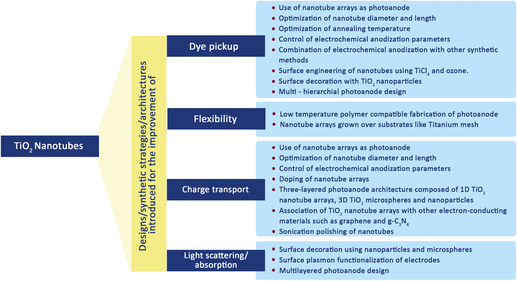 | ||
| Scheme 3 Various modifications introduced for the improvement of TiO2 nanotube based DSSC performance. | ||
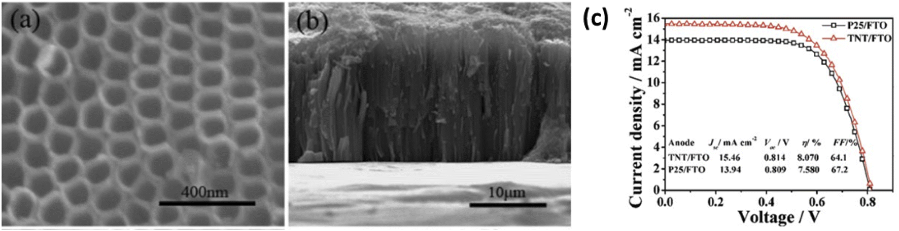 | ||
| Fig. 15 (a and b) FE-SEM images of as-prepared TNT/Ti arrays. (c) Comparison of photovoltaic performance using the same thickness (20.8 µm) of the TNT/FTO film and P25/FTO film under AM 1.5 G illumination (100 mW cm−2).206 (Reprinted with permission from ref. Lei et al., 2010. Copyright 2010 ECS – American Chemical Society.) | ||
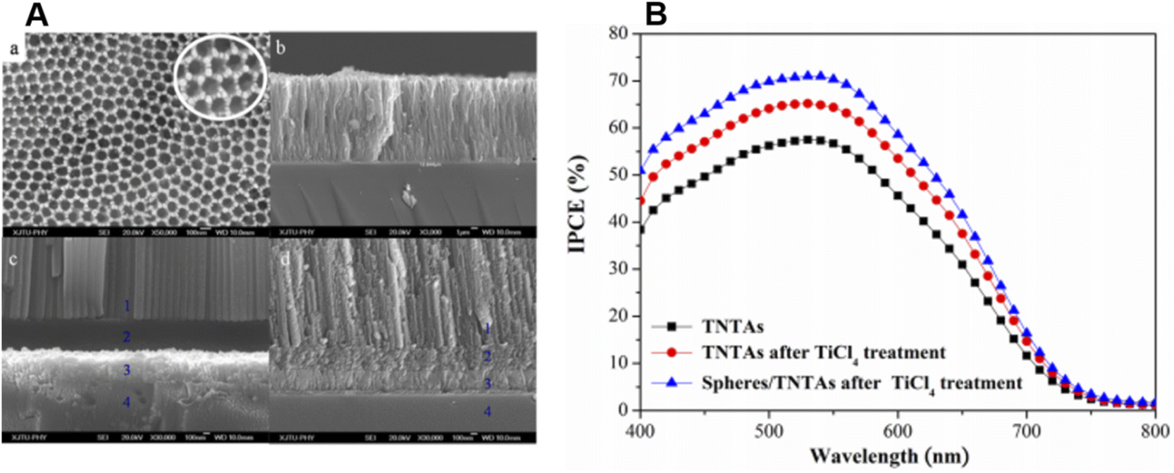 | ||
| Fig. 16 (A) SEM images of highly ordered TiO2 nanotube arrays: (a) top view; (b) cross-sectional view; (c) cross-sectional view of the bottom, before TiCl4 treatment; and (d) cross-sectional view of the bottom, after TiCl4 treatment; (B) incident photon-to-current conversion efficiency (IPCE) curves of solar cells based on TNTAs sensitized by N719.210 (Reprinted with permission from ref. He et al., 2013.Copyright 2013, American Chemical Society.) | ||
Several other associations of TiO2 nanotube arrays with other electron-conducting materials such as graphene and g-C3N4 were later introduced. Wang et al. fabricated a single-layer graphene/TiO2 nanotube array heterojunction photoanode by a wet transfer method and achieved a photon to current conversion efficiency of 4.18% which is far higher than that of pristine TiO2 nanotube photoanodes.229 The formation of a heterojunction with graphene not only reduced the bandgap but also enhanced visible light absorption. Mohammadi and co-workers modified TiO2 nanotube arrays with g-C3N4 and ZnO nanoparticles through a hydrothermal route. Even though there is no significant improvement in PCE by this composite formation, the Isc and Voc of the hybrid photoanode showed considerable improvement. In addition to the above-mentioned investigations, some distinct approaches were also attempted by researchers. For example, Lee et al. investigated the influence of various types of glass substrates on the performance of DSSCs fabricated from TiO2 nanotubes.230 They found that the photoconversion efficiency shows a significant increase with an increase in the conductivity of the glass used. Apart from the conventional cylindrical-shaped nanotubes, So et al. fabricated cone-shaped TiO2 nanotube arrays with improved photon management capability.231 When used in back side illuminated DSSCs, nanocone structures exhibited efficiencies near 8% which is the highest efficiency reported for this type of DSSC. Later in 2014, open-ended TiO2 nanotubes prepared by electrochemical anodization of Ti foil were used for DSSC fabrication by Hou et al. and these DSSCs were subjected to stability studies by I–V characterisation.220 Their results indicate that the PCE decay of the DSSCs depends on the Jsc, instead of the Voc and FF, with the extension of testing time. The stability of DSSCs mainly depends on the sealing properties and the volatile electrolyte of the devices. In 2016 Gu et al. reported the removal of the capping layer over the TiO2 nanotubes and subsequent enhancement of charge transport by sonication polishing treatment.212 This sonication polishing helped the removal of flocculent substances atop TiO2 nanotube arrays (NTAs) and also smoothened their outer surface. They have obtained an efficiency of 6.28%. Zhu et al. synthesized open-ended TiO2 nanotube arrays by removing the closed bottom caps by ball milling.232 The fast ball removal of bottom caps enhanced their surface area and the open-ended photoanode exhibited a PCE of 7.7%. As a generalisation, the common modification strategies of TiO2 nanotubes include (a) attaching light-harvesting molecules i.e. sensitization of nanotubes,206,215 (b) doping,218,222–224,233 (c) band gap engineering,202 (d) inducing electronic heterojunctions204,219,234 and (e) secondary semiconductor particle decoration.205 An overview of DSSC applications of the tubular morphology of TiO2 nanomaterials is given in Table 3.
| DSSC Type | Author | Photoelectrode and method of preparation | Sensitizer | Electrolyte | Efficiency | Ref. |
|---|---|---|---|---|---|---|
| DSSC with TiO2 nanotubes | Adachi et al. | Titania nanotubes were synthesized using molecular assemblies | N3 | 0.03 M iodine in 0.3 M lithium iodide in 3-methyl-2-oxazolidinone (NMO)/acetonitrile | 4.88% | 203 |
| DSSC with a TiO2 nanotube array | Maggie et al. | Highly ordered TiO2 nanotube arrays are made by anodization of a titanium film in a fluoride containing electrolyte | N719 | LiI, I2, N-methylbenzimidazole, guanidinium thiocyanate, and tert-butylpyridine in methoxypropionitrile (MPN) | 4.7% | 204 |
| DSSC with TiO2 nanotubes decorated with TiO2 NPs | Roy et al. | TiO2 nanotubes were prepared by anodization of Ti foil followed by annealing and TiCl4 treatment | N719 | Iodolyte R50 (Solaronix) | 3.8% | 205 |
| DSSC with a TiO2 nanotube array | Wang et al. | Highly ordered TiO2 nanotube arrays were fabricated by electrochemical anodization followed by surface engineering using TiCl4 and O2 plasma | N719 | BMIM-I, I2, TBP, and GTC in acetonitrile/valeronitrile | 7.37% | 202 |
| DSSC with a ZnO nanorod and TiO2 nanotube hybrid photoanode | Cirak et al. | Hybrid photoanode with ZnO nanorods and TiO2 nanotubes prepared through anodic oxidation followed by hydrothermal deposition | N719 | I−/I3− redox pair (Hi-30, Solaronix) | 1.67% | 228 |
| DSSC with a TiO2 nanotube array | Lei et al. | Highly ordered one-dimensional TiO2 nanotube arrays were prepared by anodization of pieces of Ti foil | N719 | I2, 1-methyl-3-propylimidazolium iodide (PMII), guanidinium thiocyanate, and tert-butylpyridine in acetonitrile and valeronitrile | 8.07% | 206 |
| DSSC with TiO2 nanotube arrays | Park et al. | Highly ordered TiO2 nanotube arrays were fabricated by anodization and transplanted on to an FTO substrate | N719 | 1-Hexyl-2,3-dimethyl-imidazolium iodide (C6DMIm), iodine (I2), lithium iodide (LiI), and 4-tert-butylpyridine in 3-methoxypropionitrile | 5.36% | 207 |
| DSSC with Nb doped TiO2 nanotube layers | Yang et al. | Nb-doped TiO2 nanotube layers were prepared by electrochemicalanodizationof Ti–Nb alloys |
N719 | I3−/I− as the redox electrolyte | 3.21% | 222 |
| DSSC with a TiO2 nanotube array/NPs | Zheng et al. | Layer-by-layer assembly of self-standing titania nanotube arrays and NPs were prepared by anodization | Ru535-bisTBA | 1,2-dimethyl-3-propyl imidazolium iodide, LiI, I2, and 4-tert-butylpyridine in acetonitrile | 8.80% | 208 |
| DSSC with Ru doped TiO2 nanotubes | So et al. | Ru doped TiO2 nanotubes were prepared by anodization of Ti–Ru alloys | D-719, (Eversolar, Taiwan) | Iodolyte R50 (Solaronix) | 5.16% | 223 |
| DSSC with B doped TiO2 nanotube arrays (TNAs) | Subramanian et al. | B doped TiO2 nanotubes were prepared by anodization of Ti foil in the presence of 0.5 wt% NH4F and 5 wt% 0.5 M boric acid in ethylene glycol solution | N719 | Iodolyte R-150 | 3.44% | 224 |
| DSSC with TiO2 nanotubes and TiO2 microspheres | He et al. | TNTAs were prepared by anodization of pieces of Ti foil in an aqueous solution containing hydrofluoric acid and TiO2 scattering microspheres were prepared via a microwave solvothermal process | N719 | I2, 1-methyl-3-propylimidazolium iodide (PMII), guanidinium thiocyanate, and tert-butylpyridine in a solution of valeronitrile and acetonitrile | 7.24% | 210 |
| DSSC with a TiO2 nanotube photoelectrode and transparent Pt counter electrode | Lee et al. | Ti layers deposited over an FTO substrate were completely anodized to obtain TiO2 nanotubes | D-719, Eversolar, Taiwan | Iolilyt SB-163(Iolitec, Germany) | 7.58% | 230 |
| DSSC with TiO2 nanotube/microsphere/NPs tri-layered photoanode | Wu et al. | Double layered photoanode with a 1D NT underlayer and 3D hierarchical upper layer was prepared by a hydrothermal method and then incorporated with hydrothermally prepared TiO2 NPs | N719 | 1-Methyl-3-propylimidazo-lium iodide (PMII), guanidinium thiocyanate, I2, LiI, and tert-butylpyridine dissolved in acetonitrile and valeronitrile | 9.10% | 211 |
| DSSC with an open ended TiO2 nanotube array | Hou et al. | Vertically oriented, high-aspect-ratio TNT arrays were prepared by two-step anodic oxidation | N719 | 1-Methyl-3-propylimidazo-lium iodide (PMII), guanidinium thiocyanate, I2, LiI, and tert-butylpyridine dissolved in acetonitrile and valeronitrile | 5.01% | 220 |
| DSSC with cone shaped TiO2 nanotube arrays | So et al. | Cone shaped TiO2 nanotubes were prepared by anodization followed by TiCl4 treatment | N719 | BMIM-I, I2, and GTC in acetonitrile/valeronitrile (SB-163, IoLiTec Inc, Germany) | 8% | 231 |
| DSSC with TiO2 nanotube arrays | Gu et al. | TiO2 NTAs were synthesized by a modified electrochemical anodic oxidation method i.e. sonication followed by anodization. Then the nanotubes were filled with Sb2S3 by chemical bath deposition | N719 | LiI, I2, and tert butylpyridine in acetonitrile | 6.28% | 212 |
| DSSC with a composite of P25 NP/TiO2 NTA/flower like TiO2 | Hu et al. | TiO2 NTAs prepared by anodization were transplanted on to a P25 coated FTO plate and then flower like TiO2 prepared hydrothermally was deposited over a P25/NTA film | N719 | LiI, I2, 4-tert-butylpyridine and 1, 2-dimethyl-3-propylimidazolium iodide (DMPII) in dry acetonitrile | 6.48% | 213 |
| DSSC with Ag nanoparticle-Functionalized open-ended freestanding TiO2nanotube arrays |
Rho et al. | TiO2 nanotube arrays prepared by anodization, with channels containing Ag NPs coated with TiO2 NPs for light scattering | N719 | I2, guanidium thiocyanate (GSCN), and 4-tert-butylpyridine (TBP) in a mixture of acetonitrile and valeronitrile | 7.05% | 214 |
| DSSC with a Au/TiO2 nanotube array/TiO2 nanoparticle photoanode | Fu et al. | “Cigar-like” Au/TiO2-nanotube-array/TiO2-nanoparticle multi-hierarchical photoanode through a novel vacuum-assisted colloid-filling approach |
N719 | LiI, I2, 1-methyl-3-hexylimidazolium iodide (HMII), N-methylbenzimidazole (NMB) and 4-tert-butylpyridine in 3-ethoxypropionitrile | 8.93% | 227 |
| DSSC with TiO2 nanotube arrays | Peighambardoust et al. | Pieces of Ti foil were degreased ultrasonically and then anodized to form TiO2 NTAs | N719 | Ionic-salt-based liquid electrolyte | 3.14% | 215 |
| DSSC with a tri-layered photoanode | Wu et al. | Tri-layered photoanode consisting of single crystal hollow TiO2 nanoparticles (HTNPs), sub-micro hollow TiO2 mesospheres (SHTMSs) and hierarchical TiO2 microspheres (HTMSs) | N719 | 1-Methyl-3-propylimidazo-lium iodide (PMII), guanidinium thiocyanate, I2, LiI, and tert-butylpyridine dissolved in acetonitrile and valeronitrile | 9.24% | 216 |
| DSSC with an open ended TiO2 nanotube array photoanode | Zhu et al. | Open ended TiO2 nanotube array photoanode was prepared by fast removal of bottom caps by mechanical ball milling | N719 | LiI, I2, 1-methyl-3- hexylimidazolium iodide (HMII), N-methylbenzimidazole (NMB), and 4-tert-butylpyridine in 3-methoxypropionitrile | 7.7% | 232 |
| DSSC with a single layer graphene–TiO2 nanotube array heterojunction | Wang et al. | Single layer graphene–TiO2 nanotube array heterojunction photoanode synthesized by a wet transfer method | N719 | Ethylene glycol solution containing NH4F and H2O | 4.18% | 229 |
3.4. Effect of one-dimensional nanomaterial morphology on electronic and charge transport properties
Compared to bulk TiO2 having a wide bandgap, one dimensional TiO2 nanostructures exhibited enhanced surface area, more active sites and quantum confinement effects. Size, specific crystal facets, morphology and alignment are the main factors determining the electronic properties of these one – dimensional TiO2 structures. In the case of nanowires, as the size reduces to the nanoscale regime, the bandgap starts increasing as per quantum confinement.66 Doping of foreign elements is the main strategy employed for the tuning of the bandgap and such dopants can align the valence band and conduction band positions in favour of the sensitizer energy levels. Also, the best DSSC performances were obtained for vertically aligned nanowire based photoanodes. In the case of nanorods, significant reduction in grain boundaries which act as electron traps caused an increment in the electron diffusion length and thereby enhanced charge transfer.174,178 The bandgap adjustment can be made in TiO2 nanorods by varying the aspect ratio of nanorods. With an increase in the aspect ratio of nanorods, there will be a downshift of the conduction band edge.66 Similarly, surface area enhancement can be achieved by introducing surface roughness and mesoporosity.235 In the case of TiO2 nanotubes, those having a wall thickness less than 5 nm are capable of manifesting quantum confinement effects.236 Only hydrothermal tubes fall under this category. The presence of Ti3+ and oxygen vacancies are another reason for enhanced charge transport. Annealing temperature is a crucial factor determining the charge transport ability of nanotubes.236 Bandgap engineering in nanotubes can be made by doping, surface adsorption, heterojunction formation and surface decoration.76,205,222,2233.5. Significance of one-dimensional TiO2 nanomorphology for exploitation of the photoanode performance
TiO2 one-dimensional (1D) morphologies were introduced as photoanode materials to overcome the limitations encountered by TiO2 nanoparticulate electrodes. These one-dimensional morphologies are found to have profound photoelectrode characteristics with certain constraints which limit their use as photoanodes. We address this problem to highlight a particular one-dimensional morphology as the best choice by analysing various TiO2 nanomaterials with 1D morphologies. A clear distinction of the best among nanowires, nanorods and nanotubes as photoanode materials requires a detailed investigation of several aspects. The main aspects to be considered are the band gap, surface area, aspect ratio, charge recombination time, transport properties and stability. In terms of surface area, nanowires, nanorods and nanotubes are inferior to zero-dimensional TiO2 nanoparticles.89 However, they possess high aspect ratios and better charge transport pathways compared to conventional multidimensional TiO2 NPs. As a result of limited surface area, the amount of dye (sensitizer) intake into these one-dimensional morphologies would be lesser. Even then, DSSCs based on TiO2 one-dimensional photoanodes exhibit better IPCEs. It was found that the TiO2 NP layer, having thrice the surface area of a TiO2 nanotube layer, exhibited a much lower IPCE compared to the nanotube layer.237 This enhancement in IPCE of nanotubes can be attributed to the much larger electron transport time prevailing in them.237 In the case of nanotube photoanode materials, the fraction of dye intake as well as electron diffusion lengths increases with an increase in the tube length. The electron diffusion lengths in nanotubes are almost thirty times that of NPs.236,237 Thus, an increased tube length can have the synergic effect of both surface area enhancement and smoother electron transport, irrespective of the high density of electron trap states in TiO2 nanotubes. Similar results are obtained in the case of TiO2 nanowires also. The best efficiencies are obtained upon arranging the nanowires vertically rather than randomly, which ensures effective contact between individual nanowires and the electrode.66 With an increase in the length of nanowires, the number of electron traps and dye loading increases. So, finding the optimal nanowire length ensures the best IPCE. The TiO2 nanorod-based photoanode exhibited an electron lifetime 8 times that of a TiO2 NP-based one.174 TiO2 nanorods showed increased electron diffusion lengths and reduced grain boundaries compared to NP-based electrodes.191 The above information leads us to the conclusion that the selection of the best one-dimensional TiO2 photoanode material among the three i.e., nanorods, nanowires and nanotubes is rather difficult. This dilemma arises due to the vast number of modifications possible over one dimensional TiO2 nanomaterials using various design strategies under different experimental conditions. Several of these investigations have led to significant and valuable findings regarding the photoanode architecture, performance parameters and stability. Upon a detailed survey of the literature, it can be seen that the combination of one dimensional TiO2 nanomaterials with other nanomaterials exhibited the best conversion efficiencies. These nanomaterials are chosen in such a way that the limitations of one-dimensional TiO2 morphologies can be made up by them. Particle decoration, heterojunction formations and multi-layered architectures are superior design strategies employed for the fabrication of modified one-dimensional TiO2 photoanodes. The limited surface area of the one-dimensional structures is improved by the addition of TiO2 NPs. These added layers cause enhanced light scattering and better dye loading capability. Decoration with metal nanoparticles makes use of surface plasmon resonance and yields better light absorption and electron transport. Heterostructures of one-dimensional TiO2 with materials having suitable band structures and electron transport properties exhibit improved efficiency. From the above literature survey (Tables 1, 2 and 3), it can be seen that top IPCE values were obtained for multi-layered photoanodes involving one-dimensional TiO2 morphologies. Each layer was incorporated with a specific function to be carried out, and such a division of labour led to enhanced outputs. Single layered one-dimensional TiO2 morphologies prepared by advanced techniques like electrospinning, anodization, etc. or a combination of these techniques with sol-gel and hydrothermal methods yield higher efficiencies.4. Summary and future prospects
This review discusses the design and working principle of various TiO2 nanomorphologies and surveys various aspects of TiO2 based photoanode materials in dye-sensitized solar cells. The total reliance of mankind on non-renewable energy sources has resulted in their depletion as well as serious environmental pollution. In this scenario, sunlight is considered a universal source of energy which is abundant in nature and free of cost. Thus, solar energy and its conversion into electricity and fuel (hydrogen) can be exploited. Solar cells which convert sunlight into electricity can be considered a future remedy for the energy crisis. In recent years a wide variety of TiO2 nanostructures have been synthesized as photoanodes for DSSC applications such as nanoparticles, nanowires, nanorods, nanotubes, etc. Due to their excellent scattering ability and high electron transport rate, these one-dimensional nanostructures are found to be efficient candidates for DSSC photoanode fabrication. By overcoming their limitations with surface area, even higher efficiencies can be achieved. The suitable band alignment of TiO2 with the sensitizer and the subsequent charge transport properties make it more attractive among other semiconductors in addition to its non-toxicity and viable functional architecture. TiO2 nanomaterials have a band gap in the UV region of solar spectra which restricts their use in the field of visible active applications. In DSSCs, the electrons in the LUMO of the dye are transferred to the conduction band of TiO2 nanomaterials. Anion and cation doping in TiO2 nanomaterials are remarkable routes to make suitable alignments of the LUMO of the dye and conduction band position of TiO2 for fast electron transfer. Recent reports show that the IR absorption capability of TiO2 can be enhanced by extending its absorption edge into the infra-red region which provides a high charge collection.116,238Conflicts of interest
There are no conflicts to declare.References
- M. Van der Hoeven, World energy outlook 2013, International Energy Agency, Tokyo, Japan, 2013 Search PubMed.
- B. Petroleum, bp. com/statisticalreview, BP, London, 2012 Search PubMed.
- BP statistical review of world energy, B. Petroleum, British Petroleum, London, UK, 2018 Search PubMed.
- J. Zhao, A. Wang, M. A. Green and F. Ferrazza, Appl. Phys. Lett., 1998, 73, 1991–1993 CrossRef CAS.
- H. Garg, in Advances in Solar Energy Technology, Springer, 1987, pp. 279–383 Search PubMed.
- M. A. Green, Y. Hishikawa, W. Warta, E. D. Dunlop, D. H. Levi, J. Hohl‐Ebinger and A. W. Ho‐Baillie, Prog. Photovolt.: Res. Appl., 2017, 25, 668–676 CrossRef.
- S. Yoon, T. Yoon, K.-S. Lee, S. Yoon, J. M. Ha and S. Choe, Sol. Energy Mater. Sol. Cells, 2009, 93, 783–788 CrossRef CAS.
- T. Suntola, MRS Bull., 1993, 18, 45–47 CrossRef CAS.
- P. Jackson, D. Hariskos, E. Lotter, S. Paetel, R. Wuerz, R. Menner, W. Wischmann and M. Powalla, Prog. Photovolt.: Res. Appl., 2011, 19, 894–897 CrossRef CAS.
- M. A. Contreras, B. Egaas, K. Ramanathan, J. Hiltner, A. Swartzlander, F. Hasoon and R. Noufi, Prog. Photovolt.: Res. Appl., 1999, 7, 311–316 CrossRef CAS.
- M. Grätzel, J. Photochem. Photobiol. C: Photochem. Rev., 2003, 4, 145–153 CrossRef.
- G. Korotcenkov, The Future of Semiconductor Oxides in Next-Generation Solar Cells, Elsevier, 2017 Search PubMed.
- M. Freitag, J. Teuscher, Y. Saygili, X. Zhang, F. Giordano, P. Liska, J. Hua, S. M. Zakeeruddin, J.-E. Moser and M. Grätzel, Nat. Photonics, 2017, 11, 372–378 CrossRef CAS.
- J. Gong, K. Sumathy, Q. Qiao and Z. Zhou, Renewable Sustainable Energy Rev., 2017, 68, 234–246 CrossRef CAS.
- B. O'regan and M. Grätzel, Nature, 1991, 353, 737–740 CrossRef.
- K. Kakiage, Y. Aoyama, T. Yano, K. Oya, J.-i. Fujisawa and M. Hanaya, Chem. Commun., 2015, 51, 15894–15897 RSC.
- S. Zhang, Study of fluorine-doped tin oxide (FTO) thin films for photovoltaics applications, Université Grenoble Alpes, ComUE, 2017 Search PubMed.
- A. Muthukumar, G. Rey, G. Giusti, V. Consonni, E. Appert, H. Roussel, A. Dakshnamoorthy and D. Bellet, AIP Conf. Proc., 2013, 1512, 710–711 CrossRef CAS.
- S. Agarwala, M. Kevin, A. Wong, C. Peh, V. Thavasi and G. Ho, ACS Appl. Mater. Interfaces, 2010, 2, 1844–1850 CrossRef CAS.
- Y. Tang, X. Pan, C. Zhang, S. Dai, F. Kong, L. Hu and Y. Sui, J. Phys. Chem. C, 2010, 114, 4160–4167 CrossRef CAS.
- J. W. Ondersma and T. W. Hamann, Coord. Chem. Rev., 2013, 257, 1533–1543 CrossRef CAS.
- G. Boschloo and A. Hagfeldt, Acc. Chem. Res., 2009, 42, 1819–1826 CrossRef CAS.
- C. H. Yoon, R. Vittal, J. Lee, W.-S. Chae and K.-J. Kim, Electrochim. Acta, 2008, 53, 2890–2896 CrossRef CAS.
- Z. Tang, J. Wu, M. Zheng, J. Huo and Z. Lan, Nano Energy, 2013, 2, 622–627 CrossRef CAS.
- K. Hara and S. Mori, Handbook of photovoltaic science and engineering, 2010, 642–674 Search PubMed.
- V. Sugathan, E. John and K. Sudhakar, Renewable Sustainable Energy Rev., 2015, 52, 54–64 CrossRef CAS.
- M. Grätzel, J. Photochem. Photobiol., A, 2004, 164, 3–14 CrossRef.
- M. A. Green, Solid-State Electron., 1981, 24, 788–789 CrossRef CAS.
- Z. Chen, T. G. Deutsch, H. N. Dinh, K. Domen, K. Emery, A. J. Forman, N. Gaillard, R. Garland, C. Heske and T. F. Jaramillo, in Photoelectrochemical Water Splitting, Springer, 2013, pp. 87–97 Search PubMed.
- M. A. Green, K. Emery, Y. Hishikawa, W. Warta and E. D. Dunlop, Prog. Photovolt.: Res. Appl., 2015, 23, 1–9 CrossRef.
- K. Zhu, N. Kopidakis, N. R. Neale, J. van de Lagemaat and A. J. Frank, J. Phys. Chem. B, 2006, 110, 25174–25180 CrossRef CAS PubMed.
- J. Kumari, N. Sanjeevadharshini, M. Dissanayake, G. Senadeera and C. Thotawatthage, Ceylon J. Sci., 2016, 45, 33–41 CrossRef.
- V. Thavasi, V. Renugopalakrishnan, R. Jose and S. Ramakrishna, Mater. Sci. Eng., R, 2009, 63, 81–99 CrossRef.
- F. De Angelis, S. Fantacci and A. Selloni, Nanotechnology, 2008, 19, 424002 CrossRef PubMed.
- P. Wang, S. M. Zakeeruddin, R. Humphry-Baker, J. E. Moser and M. Grätzel, Adv. Mater., 2003, 15, 2101–2104 CrossRef CAS.
- D. Chen, F. Huang, Y.-B. Cheng and R. A. Caruso, Adv. Mater., 2009, 21, 2206–2210 CrossRef CAS.
- K. Zhu, N. R. Neale, A. Miedaner and A. J. Frank, Nano Lett., 2007, 7, 69–74 CrossRef CAS.
- P. J. Cameron and L. M. Peter, J. Phys. Chem. B, 2003, 107, 14394–14400 CrossRef CAS.
- J. B. Baxter and E. S. Aydil, Appl. Phys. Lett., 2005, 86, 053114 CrossRef.
- C. Jiang, X. Sun, G. Lo, D. Kwong and J. Wang, Appl. Phys. Lett., 2007, 90, 263501 CrossRef.
- W. Chen, H. Zhang, I. M. Hsing and S. Yang, Electrochem. Commun., 2009, 11, 1057–1060 CrossRef CAS.
- F. Xu and L. Sun, Energy Environ. Sci., 2011, 4, 818–841 RSC.
- R. Ghosh, M. K. Brennaman, T. Uher, M.-R. Ok, E. T. Samulski, L. McNeil, T. J. Meyer and R. Lopez, ACS Appl. Mater. Interfaces, 2011, 3, 3929–3935 CrossRef CAS PubMed.
- J. Z. Ou, R. A. Rani, M.-H. Ham, M. R. Field, Y. Zhang, H. Zheng, P. Reece, S. Zhuiykov, S. Sriram and M. Bhaskaran, ACS Nano, 2012, 6, 4045–4053 Search PubMed.
- H. Zhang, Y. Wang, D. Yang, Y. Li, H. Liu, P. Liu, B. J. Wood and H. Zhao, Adv. Mater., 2012, 24, 1598–1603 Search PubMed.
- C. Prasittichai and J. T. Hupp, J. Phys. Chem. Lett., 2010, 1, 1611–1615 Search PubMed.
- E. Ramasamy and J. Lee, J. Phys. Chem. C, 2010, 114, 22032–22037 Search PubMed.
- H. Song, K.-H. Lee, H. Jeong, S. H. Um, G.-S. Han, H. S. Jung and G. Y. Jung, Nanoscale, 2013, 5, 1188–1194 Search PubMed.
- C. W. Kim, S. P. Suh, M. J. Choi, Y. S. Kang and Y. S. Kang, J. Mater. Chem. A, 2013, 1, 11820–11827 Search PubMed.
- Y. S. Wang, T. T. Chen, Y. J. Huang, T. P. Huang, Y. Y. Lee, H. T. Chiu and C. Y. Lee, J. Chin. Chem. Soc., 2013, 60, 1437–1441 Search PubMed.
- H. Zheng, Y. Tachibana and K. Kalantar-zadeh, Langmuir, 2010, 26, 19148–19152 Search PubMed.
- N. Prabhu, S. Agilan, N. Muthukumarasamy and T. Senthil, J. Mater. Sci.: Mater. Electron., 2014, 25, 5288–5295 Search PubMed.
- M. Rashad and A. Shalan, Appl. Phys. A, 2014, 116, 781–788 Search PubMed.
- B. Tan, E. Toman, Y. Li and Y. Wu, J. Am. Chem. Soc., 2007, 129, 4162–4163 Search PubMed.
- J. Chen, L. Lu and W. Wang, J. Phys. Chem. C, 2012, 116, 10841–10847 Search PubMed.
- D. W. Kim, S. S. Shin, I. S. Cho, S. Lee, D. H. Kim, C. W. Lee, H. S. Jung and K. S. Hong, Nanoscale, 2012, 4, 557–562 Search PubMed.
- S. Yang, Y. Hou, J. Xing, B. Zhang, F. Tian, X. H. Yang and H. G. Yang, Chem.–Eur. J., 2013, 19, 9366–9370 Search PubMed.
- A. R. Tanyi, P. Ekanayake, A. L. Tan, D. J. Young and D. Peiris, 2016.
- D. Zheng, J. Xiong, P. Guo, Y. Li and H. Gu, J. Nanosci. Nanotechnol., 2016, 16, 613–618 Search PubMed.
- L. De Marco, D. Calestani, A. Qualtieri, R. Giannuzzi, M. Manca, P. Ferro, G. Gigli, A. Listorti and R. Mosca, Sol. Energy Mater. Sol. Cells, 2017, 168, 227–233 Search PubMed.
- I. C. Maurya, A. K. Gupta, P. Srivastava and L. Bahadur, J. Solid State Electrochem., 2017, 21, 1229–1241 Search PubMed.
- H. Sun, L. Sun, T. Sugiura, M. S. White, P. Stadler, N. S. Sariciftci, A. Masuhara and T. Yoshida, Electrochemistry, 2017, 85, 253–261 Search PubMed.
- R. K. Chava and M. Kang, Improving the photovoltaic conversion efficiency of ZnO based dye sensitized solar cells by indium doping, J. Alloys Compd., 2016, 692, 67–76 Search PubMed.
- X. Bokhimi, A. Morales, M. Aguilar, J. A. Toledo-Antonio and F. Pedraza, Int. J. Hydrogen Energy, 2001, 26, 1279–1287 Search PubMed.
- M. Posternak, A. Baldereschi and B. Delley, Structural and Electronic Properties of Monoclinic TiO2 (B) Polymorph, 2007 Search PubMed.
- X. Wang, Z. Li, J. Shi and Y. Yu, Chem. Rev., 2014, 114, 9346–9384 Search PubMed.
- M. Kapilashrami, Y. Zhang, Y.-S. Liu, A. Hagfeldt and J. Guo, Chem. Rev., 2014, 114, 9662–9707 Search PubMed.
- D. Reyes-Coronado, G. Rodríguez-Gattorno, M. E. Espinosa-Pesqueira, C. Cab, R. d. Coss and G. Oskam, Nanotechnology, 2008, 19, 145605 Search PubMed.
- M. Shakeel Ahmad, A. K. Pandey and N. Abd Rahim, Renewable Sustainable Energy Rev., 2017, 77, 89–108 Search PubMed.
- Y. Hao, Y. Saygili, J. Cong, A. Eriksson, W. Yang, J. Zhang, E. Polanski, K. Nonomura, S. M. Zakeeruddin, M. Grätzel, A. Hagfeldt and G. Boschloo, ACS Appl. Mater. Interfaces, 2016, 8, 32797–32804 Search PubMed.
- K. Madhusudan Reddy, S. V. Manorama and A. Ramachandra Reddy, Mater. Chem. Phys., 2003, 78, 239–245 Search PubMed.
- A. K. Chandiran, M. Abdi-Jalebi, M. K. Nazeeruddin and M. Grätzel, ACS Nano, 2014, 8, 2261–2268 Search PubMed.
- E. C. Muniz, M. S. Góes, J. J. Silva, J. A. Varela, E. Joanni, R. Parra and P. R. Bueno, Ceram. Int., 2011, 37, 1017–1024 Search PubMed.
- I. S. Cho, Z. Chen, A. J. Forman, D. R. Kim, P. M. Rao, T. F. Jaramillo and X. Zheng, Nano Lett., 2011, 11, 4978–4984 Search PubMed.
- X. Feng, K. Shankar, O. K. Varghese, M. Paulose, T. J. Latempa and C. A. Grimes, Nano Lett., 2008, 8, 3781–3786 Search PubMed.
- P. Roy, D. Kim, K. Lee, E. Spiecker and P. Schmuki, Nanoscale, 2010, 2, 45–59 Search PubMed.
- M. Sabet, M. Salavati-Niasari and O. Amiri, Electrochim. Acta, 2014, 117, 504–520 Search PubMed.
- R. L. Z. Hoye, K. P. Musselman and J. L. MacManus-Driscoll, APL Mater., 2013, 1, 060701 Search PubMed.
- B. Roose, S. Pathak and U. Steiner, Chem. Soc. Rev., 2015, 44, 8326–8349 Search PubMed.
- H. Zhang and J. F. Banfield, Chem. Rev., 2014, 114, 9613–9644 Search PubMed.
- T. Umebayashi, T. Yamaki, H. Itoh and K. Asai, J. Phys. Chem. Solids, 2002, 63, 1909–1920 Search PubMed.
- M. A. Barakat and R. Kumar, Photocatalytic Activity Enhancement of Titanium Dioxide Nanoparticles: Degradation of Pollutants in Wastewater, Springer International Publishing, 2015 Search PubMed.
- F. De Angelis, S. Fantacci, A. Selloni, M. K. Nazeeruddin and M. Grätzel, J. Phys. Chem. C, 2010, 114, 6054–6061 Search PubMed.
- S. Meng and E. Kaxiras, Nano Lett., 2010, 10, 1238–1247 Search PubMed.
- J. C. Yu, J. Yu, W. Ho, Z. Jiang and L. Zhang, Chem. Mater., 2002, 14, 3808–3816 Search PubMed.
- A. A. Murashkina, P. D. Murzin, A. V. Rudakova, V. K. Ryabchuk, A. V. Emeline and D. W. Bahnemann, J. Phys. Chem. C, 2015, 119, 24695–24703 Search PubMed.
- M.-J. Jeng, Y.-L. Wung, L.-B. Chang and L. Chow, Int. J. Photoenergy, 2013, 2013, 9 Search PubMed.
- X. Hua, Z. Liu, P. G. Bruce and C. P. Grey, J. Am. Chem. Soc., 2015, 137, 13612–13623 Search PubMed.
- M. Ge, C. Cao, J. Huang, S. Li, Z. Chen, K.-Q. Zhang, S. S. Al-Deyab and Y. Lai, J. Mater. Chem. A, 2016, 4, 6772–6801 Search PubMed.
- A. Lamberti, A. Sacco, S. Bianco, D. Manfredi, F. Cappelluti, S. Hernandez, M. Quaglio and C. F. Pirri, Phys. Chem. Chem. Phys., 2013, 15, 2596–2602 Search PubMed.
- H. Wang, H. Li, J. Wang, J. Wu, D. Li, M. Liu and P. Su, Electrochim. Acta, 2014, 137, 744–750 Search PubMed.
- M. M. Momeni, Rare Met., 2017, 36, 865–871 Search PubMed.
- J.-Y. Park, C.-S. Kim, K. Okuyama, H.-M. Lee, H.-D. Jang, S.-E. Lee and T. Kim, Copper and nitrogen doping on TiO2 photoelectrodes and their functions in dye-sensitized solar cells, J. Power Sources, 2016 Search PubMed.
- S. Iwamoto, Y. Sazanami, M. Inoue, T. Inoue, T. Hoshi, K. Shigaki, M. Kaneko and A. Maenosono, ChemSusChem, 2008, 1, 401–403 Search PubMed.
- M. Nada, T. Gonda, Q. Shen, H. Shimada, T. Toyoda and N. Kobayashi, Jpn. J. Appl. Phys., 2009, 48, 025505 Search PubMed.
- M. Pan, H. Liu, Z. Yao and X. Zhong, J. Nanomater., 2015, 2015, 5 Search PubMed.
- T.-V. Nguyen, H.-C. Lee, M. A. Khan and O.-B. Yang, Sol. Energy, 2007, 81, 529–534 Search PubMed.
- H. Tian, L. Hu, C. Zhang, S. Chen, J. Sheng, L. Mo, W. Liu and S. Dai, J. Mater. Chem., 2011, 21, 863–868 Search PubMed.
- M. Wang, S. Bai, A. Chen, Y. Duan, Q. Liu, D. Li and Y. Lin, Electrochim. Acta, 2012, 77, 54–59 Search PubMed.
- T. Ma, M. Akiyama, E. Abe and I. Imai, Nano Lett., 2005, 5, 2543–2547 Search PubMed.
- H. Tian, L. Hu, C. Zhang, W. Liu, Y. Huang, L. Mo, L. Guo, J. Sheng and S. Dai, J. Phys. Chem. C, 2010, 114, 1627–1632 Search PubMed.
- Q. Sun, J. Zhang, P. Wang, J. Zheng, X. Zhang, Y. Cui, J. Feng and Y. Zhu, J. Renewable Sustainable Energy, 2012, 4, 023104 Search PubMed.
- B. Yacoubi, L. Samet, J. Bennaceur, A. Lamouchi and R. Chtourou, Properties of transition metal doped-titania electrodes: impact on efficiency of amorphous and nanocrystalline dye-sensitized solar cells, Mater. Sci. Semicond. Process., 2014, 30, 361–367 Search PubMed.
- R. Li, Y. Zhao, R. Hou, X. Ren, S. Yuan, Y. Lou, Z. Wang, D. Li and L. Shi, J. Photochem. Photobiol., A, 2016, 319–320, 62–69 Search PubMed.
- Y. Duan, N. Fu, Q. Liu, Y. Fang, X. Zhou, J. Zhang and Y. Lin, J. Phys. Chem. C, 2012, 116, 8888–8893 Search PubMed.
- W.-W. Xu, S.-Y. Dai, L.-H. Hu, L.-Y. Liang and K.-J. Wang, Chin. Phys. Lett., 2006, 23, 2288 Search PubMed.
- Z. Zhang, G. Li, Z. Cui, K. Zhang, Y. Feng and S. Meng, J. Solid State Chem., 2016, 237, 242–247 Search PubMed.
- L. Wei, Y. Yang, X. Xia, R. Fan, T. Su, Y. Shi, J. Yu, L. Li and Y. Jiang, RSC Adv., 2015, 5, 70512–70521 Search PubMed.
- J. C. Zhang, Z. Y. Han, Q. Y. Li, X. Y. Yang, Y. Yu and W. L. Cao, J. Phys. Chem. Solids, 2011, 72, 1239–1244 Search PubMed.
- Y. Jiang, Y. Chen, B. Zhang and Y. Feng, J. Electrochem. Soc., 2016, 163, F1133–F1138 Search PubMed.
- E. M. Jin, S. M. Jeong, H.-C. Kang and H.-B. Gu, ECS J. Solid State Sci. Technol., 2016, 5, Q109–Q114 Search PubMed.
- A. Ahmad, S. Buzby, C. Ni and S. I. Shah, J. Nanosci. Nanotechnol., 2008, 8, 2410–2418 Search PubMed.
- T. Bak, M. K. Nowotny, L. R. Sheppard and J. Nowotny, J. Phys. Chem. C, 2008, 112, 12981–12987 Search PubMed.
- F. Giordano, A. Abate, J. P. Correa Baena, M. Saliba, T. Matsui, S. H. Im, S. M. Zakeeruddin, M. K. Nazeeruddin, A. Hagfeldt and M. Graetzel, Nat. Commun., 2016, 7, 10379 Search PubMed.
- W. Guo, Y. Shen, L. Wu, Y. Gao and T. Ma, J. Phys. Chem. C, 2011, 115, 21494–21499 Search PubMed.
- S. G. Ullattil, A. V. Thelappurath, S. N. Tadka, J. Kavil, B. K. Vijayan and P. Periyat, Sol. Energy, 2017, 155, 490–495 Search PubMed.
- B. O'Regan and M. Gratzel, Nature, 1991, 353, 737–740 Search PubMed.
- R. Amadelli, R. Argazzi, C. A. Bignozzi and F. Scandola, J. Am. Chem. Soc., 1990, 112, 7099–7103 Search PubMed.
- S. Ito, T. N. Murakami, P. Comte, P. Liska, C. Grätzel, M. K. Nazeeruddin and M. Grätzel, Thin Solid Films, 2008, 516, 4613–4619 Search PubMed.
- Y.-J. Chang, E.-H. Kong, Y.-C. Park and H. M. Jang, J. Mater. Chem. A, 2013, 1, 9707–9713 Search PubMed.
- N. Mir and M. Salavati-Niasari, Mater. Res. Bull., 2013, 48, 1660–1667 Search PubMed.
- S. Iijima, Nature, 1991, 354, 56–58 Search PubMed.
- M. Law, L. E. Greene, J. C. Johnson, R. Saykally and P. Yang, Nat. Mater., 2005, 4, 455–459 Search PubMed.
- E. Enache-Pommer, J. E. Boercker and E. S. Aydil, Appl. Phys. Lett., 2007, 91, 123116 Search PubMed.
- J.-Y. Liao, B.-X. Lei, H.-Y. Chen, D.-B. Kuang and C.-Y. Su, Energy Environ. Sci., 2012, 5, 5750–5757 Search PubMed.
- X. Cai, H. Wu, S. Hou, M. Peng, X. Yu and D. Zou, ChemSusChem, 2014, 7, 474–482 Search PubMed.
- W. Liu, H. Lu, M. Zhang and M. Guo, Appl. Surf. Sci., 2015, 347, 214–223 Search PubMed.
- X. Sheng, D. He, J. Yang, K. Zhu and X. Feng, Nano Lett., 2014, 14, 1848–1852 Search PubMed.
- A. M. Bakhshayesh, M. R. Mohammadi, H. Dadar and D. J. Fray, Electrochim. Acta, 2013, 90, 302–308 Search PubMed.
- D. K. Roh, W. S. Chi, S. H. Ahn, H. Jeon and J. H. Kim, ChemSusChem, 2013, 6, 1384–1391 Search PubMed.
- Z.-j. Zhou, J.-q. Fan, X. Wang, W.-h. Zhou, Z.-l. Du and S.-x. Wu, ACS Appl. Mater. Interfaces, 2011, 3, 4349–4353 Search PubMed.
- C. Zha, L. Shen, X. Zhang, Y. Wang, B. A. Korgel, A. Gupta and N. Bao, ACS Appl. Mater. Interfaces, 2014, 6, 122–129 Search PubMed.
- F.-T. Kong, S.-Y. Dai and K.-J. Wang, Adv. OptoElectron., 2007, 2007, 13 Search PubMed.
- W.-Q. Wu, Y.-F. Xu, C.-Y. Su and D.-B. Kuang, Energy Environ. Sci., 2014, 7, 644–649 Search PubMed.
- W.-Q. Wu, Y.-F. Xu, H.-S. Rao, C.-Y. Su and D.-B. Kuang, J. Am. Chem. Soc., 2014, 136, 6437–6445 Search PubMed.
- H. Li, Q. Yu, Y. Huang, C. Yu, R. Li, J. Wang, F. Guo, S. Jiao, S. Gao and Y. Zhang, ACS Appl. Mater. Interfaces, 2016, 8, 13384–13391 Search PubMed.
- Y.-C. Yen, P.-H. Chen, J.-Z. Chen, J.-A. Chen and K.-J. Lin, ACS Appl. Mater. Interfaces, 2015, 7, 1892–1898 Search PubMed.
- K.-W. Lee, M. Kim, J.-M. Kim, J. J. Kim and I.-H. Lee, J. Alloys Compd., 2016, 656, 568–572 Search PubMed.
- S. Jin, E. Shin and J. Hong, Nanomaterials, 2017, 7, 315 Search PubMed.
- E. Shin, S. Jin and J. Hong, Appl. Surf. Sci., 2017, 416, 353–357 Search PubMed.
- Z. Li, H. Yang, F. Wu, J. Fu, L. Wang and W. Yang, Electron. Mater. Lett., 2017, 13, 174–178 Search PubMed.
- G. Liu, H. Wang, M. Wang, W. Liu, R. E. Anugrah Ardhi, D. Zou and J. K. Lee, Electrochim. Acta, 2018, 267, 34–40 Search PubMed.
- S. Ni, D. Wang, F. Guo, S. Jiao, Y. Zhang, J. Wang, B. Wang, L. Yuan, L. Zhang and L. Zhao, J. Cryst. Growth, 2019, 505, 62–68 Search PubMed.
- P. Makal and D. Das, ACS Omega, 2021, 6, 4362–4373 Search PubMed.
- P. Makal and D. Das, Mater. Chem. Phys., 2021, 266, 124520 Search PubMed.
- D. Jiang, Y. Hao, R. Shen, S. Ghazarian, A. Ramos and F. Zhou, ACS Appl. Mater. Interfaces, 2013, 5, 11906–11912 Search PubMed.
- J. Jiu, S. Isoda, F. Wang and M. Adachi, J. Phys. Chem. B, 2006, 110, 2087–2092 Search PubMed.
- J. Jiu, F. Wang, S. Isoda and M. Adachi, Chem. Lett., 2005, 34, 1506–1507 Search PubMed.
- L. De Marco, M. Manca, R. Giannuzzi, F. Malara, G. Melcarne, G. Ciccarella, I. Zama, R. Cingolani and G. Gigli, J. Phys. Chem. C, 2010, 114, 4228–4236 Search PubMed.
- H. Hafez, Z. Lan, Q. Li and J. Wu, Nanotechnol., Sci. Appl., 2010, 3, 45 Search PubMed.
- K. Fan, W. Zhang, T. Peng, J. Chen and F. Yang, J. Phys. Chem. C, 2011, 115, 17213–17219 Search PubMed.
- Q. Huang, G. Zhou, L. Fang, L. Hu and Z.-S. Wang, Energy Environ. Sci., 2011, 4, 2145–2151 Search PubMed.
- F. Shao, J. Sun, L. Gao, S. Yang and J. Luo, J. Phys. Chem. C, 2011, 115, 1819–1823 Search PubMed.
- J. Liu, Y. Wang and D. Sun, Renewable Energy, 2012, 38, 214–218 Search PubMed.
- Z.-H. Liu, X.-J. Su, G.-L. Hou, S. Bi, Z. Xiao and H.-P. Jia, J. Power Sources, 2012, 218, 280–285 Search PubMed.
- Y. Rui, Y. Li, Q. Zhang and H. Wang, Nanoscale, 2013, 5, 12574–12581 Search PubMed.
- H. Yu, J. Pan, Y. Bai, X. Zong, X. Li and L. Wang, Chem.–Eur. J., 2013, 19, 13569–13574 Search PubMed.
- W. Zhang, Y. Xie, D. Xiong, X. Zeng, Z. Li, M. Wang, Y.-B. Cheng, W. Chen, K. Yan and S. Yang, ACS Appl. Mater. Interfaces, 2014, 6, 9698–9704 Search PubMed.
- J. Liu, J. Luo, W. Yang, Y. Wang, L. Zhu, Y. Xu, Y. Tang, Y. Hu, C. Wang and Y. Chen, J. Mater. Sci. Technol., 2015, 31, 106–109 Search PubMed.
- S. Kathirvel, C. Su, Y.-J. Shiao, Y.-F. Lin, B.-R. Chen and W.-R. Li, Sol. Energy, 2016, 132, 310–320 Search PubMed.
- B. Liu and E. S. Aydil, J. Am. Chem. Soc., 2009, 131, 3985–3990 Search PubMed.
- T. Ohno, K. Sarukawa, K. Tokieda and M. Matsumura, Morphology of a TiO2 Photocatalyst (Degussa, P-25) Consisting of Anatase and Rutile Crystalline Phases, J. Catal., 200, 203, 82–86 Search PubMed.
- M. Guli, Z. Hu, J. Yao, Z. Zhou, X. Sun and L. Chen, Mater. Technol., 2017, 32, 239–244 Search PubMed.
- A. Hu, J. Wang, S. Qu, Z. Zhong, S. Wang and G. Liang, J. Mater. Sci.: Mater. Electron., 2017, 28, 3415–3422 Search PubMed.
- M. Iraj, F. D. Nayeri, E. Asl-Soleimani and K. Narimani, J. Alloys Compd., 2016, 659, 44–50 Search PubMed.
- H.-Y. Chen, T.-L. Zhang, J. Fan, D.-B. Kuang and C.-Y. Su, ACS Appl. Mater. Interfaces, 2013, 5, 9205–9211 Search PubMed.
- F. Shao, J. Sun, L. Gao, J. Chen and S. Yang, RSC Adv., 2014, 4, 7805–7810 Search PubMed.
- W. Li, J. Yang, Q. Jiang, Y. Luo, Y. Hou, S. Zhou and Z. Zhou, J. Power Sources, 2015, 284, 428–434 Search PubMed.
- H. Sayahi, K. Aghapoor, F. Mohsenzadeh, M. Mohebi Morad and H. R. Darabi, Sol. Energy, 2021, 215, 311–320 Search PubMed.
- S. Ghannadi, H. Abdizadeh, A. Rakhsha and M. R. Golobostanfard, Mater. Chem. Phys., 2021, 258, 123893 Search PubMed.
- S. Chatterjee, W. A. Webre, S. Patra, B. Rout, G. A. Glass, F. D'Souza and S. Chatterjee, J. Alloys Compd., 2020, 826, 154188 Search PubMed.
- V. S. Saji and M. Pyo, Thin Solid Films, 2010, 518, 6542–6546 Search PubMed.
- K. Fujihara, A. Kumar, R. Jose, S. Ramakrishna and S. Uchida, Nanotechnology, 2007, 18, 365709 Search PubMed.
- B. H. Lee, M. Y. Song, S.-Y. Jang, S. M. Jo, S.-Y. Kwak and D. Y. Kim, J. Phys. Chem. C, 2009, 113, 21453–21457 Search PubMed.
- L. Yang and W. W. F. Leung, Adv. Mater., 2013, 25, 1792–1795 Search PubMed.
- H. Wang, Y. Bai, Q. Wu, W. Zhou, H. Zhang, J. Li and L. Guo, Phys. Chem. Chem. Phys., 2011, 13, 7008–7013 Search PubMed.
- W. Guo, C. Xu, X. Wang, S. Wang, C. Pan, C. Lin and Z. L. Wang, J. Am. Chem. Soc., 2012, 134, 4437–4441 Search PubMed.
- H. Wang, M. Liu, M. Zhang, P. Wang, H. Miura, Y. Cheng and J. Bell, Phys. Chem. Chem. Phys., 2011, 13, 17359–17366 Search PubMed.
- X. Gu, Y. Zhao and Y. Qiang, J. Mater. Sci.: Mater. Electron., 2012, 23, 1373–1377 Search PubMed.
- Y. Zhao, X. Gu and Y. Qiang, Thin Solid Films, 2012, 520, 2814–2818 Search PubMed.
- M. Ghaffari, M. B. Cosar, H. I. Yavuz, M. Ozenbas and A. K. Okyay, Electrochim. Acta, 2012, 76, 446–452 Search PubMed.
- T. Yuan, H. Lu, B. Dong, L. Zhao, L. Wan, S. Wang and Z. Xu, J. Mater. Sci.: Mater. Electron., 2015, 26, 1332–1337 Search PubMed.
- Q. Yao, J. Liu, Q. Peng, X. Wang and Y. Li, Chem.–Asian J., 2006, 1, 737–741 Search PubMed.
- S.-M. Wang, W.-W. Dong, R.-H. Tao, Z.-H. Deng, J.-Z. Shao, L.-H. Hu, J. Zhu and X.-D. Fang, J. Power Sources, 2013, 235, 193–201 Search PubMed.
- X. Chen, Q. Du, W. Yang, W. Liu, Z. Miao and P. Yang, J. Solid State Electrochem., 2018, 22, 685–691 Search PubMed.
- N. Sriharan, T. S. Senthil, M. Kang and N. M. Ganesan, Appl. Phys. A, 2019, 125, 118 Search PubMed.
- M. R. Subramaniam, D. Kumaresan, S. Jothi, J. D. McGettrick and T. M. Watson, Appl. Surf. Sci., 2018, 428, 439–447 Search PubMed.
- A. Roy, S. Mukhopadhyay, P. S. Devi and S. Sundaram, ACS Omega, 2019, 4, 1130–1138 Search PubMed.
- Y. Tang, C. Wang, Y. Hu, L. Huang, J. Fu and W. Yang, Superlattices Microstruct., 2016, 89, 1–6 Search PubMed.
- R. Jose, A. Kumar, V. Thavasi and S. Ramakrishna, Nanotechnology, 2008, 19, 424004 Search PubMed.
- S. H. Kang, S. H. Choi, M. S. Kang, J. Y. Kim, H. S. Kim, T. Hyeon and Y. E. Sung, Adv. Mater., 2008, 20, 54–58 Search PubMed.
- Z. Wang, H. Wang, B. Liu, W. Qiu, J. Zhang, S. Ran, H. Huang, J. Xu, H. Han and D. Chen, ACS Nano, 2011, 5, 8412–8419 Search PubMed.
- M. Yang, B. Ding, S. Lee and J.-K. Lee, J. Phys. Chem. C, 2011, 115, 14534–14541 Search PubMed.
- G. K. Mor, O. K. Varghese, M. Paulose, K. Shankar and C. A. Grimes, Sol. Energy Mater. Sol. Cells, 2006, 90, 2011–2075 Search PubMed.
- Q. Zhou, Z. Fang, J. Li and M. Wang, Microporous Mesoporous Mater., 2015, 202, 22–35 Search PubMed.
- E. Ghadiri, N. Taghavinia, S. M. Zakeeruddin, M. Grätzel and J.-E. Moser, Nano Lett., 2010, 10, 1632–1638 Search PubMed.
- J. R. Jennings, A. Ghicov, L. M. Peter, P. Schmuki and A. B. Walker, J. Am. Chem. Soc., 2008, 130, 13364–13372 Search PubMed.
- S. Li, Y. Liu, G. Zhang, X. Zhao and J. Yin, Thin Solid Films, 2011, 520, 689–693 Search PubMed.
- P. Roy, S. Berger and P. Schmuki, Angew. Chem., Int. Ed., 2011, 50, 2904–2939 Search PubMed.
- A. Ghicov, S. P. Albu, R. Hahn, D. Kim, T. Stergiopoulos, J. Kunze, C.-A. Schiller, P. Falaras and P. Schmuki, Chem.–Asian J., 2009, 4, 520–525 Search PubMed.
- S. H. Kang, J.-Y. Kim, Y. Kim, H. S. Kim and Y.-E. Sung, J. Phys. Chem. C, 2007, 111, 9614–9623 Search PubMed.
- J. Wang and Z. Lin, Chem. Mater., 2009, 22, 579–584 Search PubMed.
- M. Adachi, Y. Murata, I. Okada and S. Yoshikawa, J. Electrochem. Soc., 2003, 150, G488–G493 Search PubMed.
- P. Maggie, S. Karthik, K. V. Oomman, K. M. Gopal and A. G. Craig, J. Phys. D: Appl. Phys., 2006, 39, 2498 Search PubMed.
- P. Roy, D. Kim, I. Paramasivam and P. Schmuki, Electrochem. Commun., 2009, 11, 1001–1004 Search PubMed.
- B.-X. Lei, J.-Y. Liao, R. Zhang, J. Wang, C.-Y. Su and D.-B. Kuang, J. Phys. Chem. C, 2010, 114, 15228–15233 Search PubMed.
- H. Park, W.-R. Kim, H.-T. Jeong, J.-J. Lee, H.-G. Kim and W.-Y. Choi, Sol. Energy Mater. Sol. Cells, 2011, 95, 184–189 Search PubMed.
- Q. Zheng, H. Kang, J. Yun, J. Lee, J. H. Park and S. Baik, ACS Nano, 2011, 5, 5088–5093 Search PubMed.
- Z. Yi, Y. Zeng, H. Wu, X. Chen, Y. Fan, H. Yang, Y. Tang, Y. Yi, J. Wang and P. Wu, Results Phys., 2019, 15, 102609 Search PubMed.
- Z. He, W. Que, P. Sun and J. Ren, ACS Appl. Mater. Interfaces, 2013, 5, 12779–12783 Search PubMed.
- W.-Q. Wu, Y.-F. Xu, H.-S. Rao, C.-Y. Su and D.-B. Kuang, J. Phys. Chem. C, 2014, 118, 16426–16432 Search PubMed.
- K. Gu, P. Zhong, M. Guo, J. Ma, Q. Jiang, S. Zhang, X. Zhou, Y. Xie, X. Ma and Y. Wang, J. Solid State Electrochem., 2016, 20, 3337–3348 Search PubMed.
- J.-H. Hu, S.-Q. Tong, Y.-P. Yang, J.-J. Cheng, L. Zhao and J.-X. Duan, Acta Metall. Sin. (Engl. Lett.), 2016, 29, 840–847 Search PubMed.
- W.-Y. Rho, M.-H. Chun, H.-S. Kim, H.-M. Kim, J. S. Suh and B.-H. Jun, Nanomaterials, 2016, 6, 117 Search PubMed.
- N.-S. Peighambardoust, S. Khameneh-Asl and H. Azimi, Appl. Phys. A, 2017, 123, 345 Search PubMed.
- M. Wu, J. Khan, J. Gu, S. He, X. Li, G. Ahmed, Z. Liu, M. N. Akhtar and W. Mai, Nanoscale, 2017 Search PubMed.
- V. Madurai Ramakrishnan, N. Muthukumarasamy, P. Balraju, S. Pitchaiya, D. Velauthapillai and A. Pugazhendhi, Int. J. Hydrogen Energy, 2020, 45, 15441–15452 Search PubMed.
- X. Tang and D. Li, J. Phys. Chem. C, 2008, 112, 5405–5409 Search PubMed.
- J.-H. Kim, K. Zhu, Y. Yan, C. L. Perkins and A. J. Frank, Nano Lett., 2010, 10, 4099–4104 Search PubMed.
- Z. Hou, W. Que, J. Ren, Y. Xing, H. M. A. Javed, T. Zhou and L. Bing Kong, Ceram. Int., 2015, 41, S719–S724 Search PubMed.
- G. K. Mor, K. Shankar, M. Paulose, O. K. Varghese and C. A. Grimes, Nano Lett., 2006, 6, 215–218 Search PubMed.
- M. Yang, D. Kim, H. Jha, K. Lee, J. Paul and P. Schmuki, Chem. Commun., 2011, 47, 2032–2034 Search PubMed.
- S. So, K. Lee and P. Schmuki, Phys. Status Solidi Rapid Res. Lett., 2012, 6, 169–171 Search PubMed.
- A. Subramanian and H.-W. Wang, Appl. Surf. Sci., 2012, 258, 6479–6484 Search PubMed.
- J. Chen, M. Guo, H. Su, J. Zhang, L. Liu, H. Huang and K. Xie, J. Appl. Electrochem., 2018, 48, 1139–1149 Search PubMed.
- M. Guo, J. Chen, J. Zhang, H. Su, L. Liu, N. Fu and K. Xie, Electrochim. Acta, 2018, 263, 373–381 Search PubMed.
- N. Fu, X. Jiang, D. Chen, Y. Duan, G. Zhang, M. Chang, Y. Fang and Y. Lin, J. Power Sources, 2019, 439, 227076 Search PubMed.
- B. Bozkurt Çırak, Ç. Eden, Y. Erdoğan, Z. Demir, K. V. Özdokur, B. Caglar, S. Morkoç Karadeniz, T. Kılınç, A. Ercan Ekinci and Ç. Çırak, Optik, 2020, 203, 163963 Search PubMed.
- J. Wang, X. Nie, W. Wang, Z. Zhao, L. Li and Z. Zhang, Optik, 2021, 242, 167245 Search PubMed.
- K. Lee, R. Kirchgeorg and P. Schmuki, J. Phys. Chem. C, 2014, 118, 16562–16566 Search PubMed.
- S. So, A. Kriesch, U. Peschel and P. Schmuki, J. Mater. Chem. A, 2015, 3, 12603–12608 Search PubMed.
- W. Zhu, Y. Liu, A. Yi, M. Zhu, W. Li and N. Fu, Electrochim. Acta, 2019, 299, 339–345 Search PubMed.
- T. Lopez-Luke, A. Wolcott, L.-p. Xu, S. Chen, Z. Wen, J. Li, E. De La Rosa and J. Z. Zhang, J. Phys. Chem. C, 2008, 112, 1282–1292 Search PubMed.
- G. K. Mor, S. Kim, M. Paulose, O. K. Varghese, K. Shankar, J. Basham and C. A. Grimes, Nano Lett., 2009, 9, 4250–4257 Search PubMed.
- L. De Marco, M. Manca, R. Giannuzzi, M. R. Belviso, P. D. Cozzoli and G. Gigli, Energy Environ. Sci., 2013, 6, 1791–1795 Search PubMed.
- K. Lee, A. Mazare and P. Schmuki, Chem. Rev., 2014, 114, 9385–9454 Search PubMed.
- R. P. Lynch, A. Ghicov and P. Schmuki, J. Electrochem. Soc., 2010, 157, G76 Search PubMed.
- S. G. Ullattil and P. Periyat, Sol. Energy, 2017, 147, 99–105 Search PubMed.
| This journal is © The Royal Society of Chemistry 2022 |