
 Open Access Article
 This Open Access Article is licensed under a Creative Commons Attribution-Non Commercial 3.0 Unported Licence
MoS2 oxidative etching caught in the act: formation of single (MoO3)n molecules†
Saeed
Sovizi
 a,
Sergio
Tosoni
*b and
Robert
Szoszkiewicz
*a
a,
Sergio
Tosoni
*b and
Robert
Szoszkiewicz
*a
aFaculty of Chemistry, Biological and Chemical Research Centre, University of Warsaw, Żwirki I Wigury 101, 02-089 Warsaw, Poland. E-mail: rszoszkiewicz@chem.uw.edu.pl
bDipartimento di Scienza dei materiali, Università di Milano-Bicocca, via Roberto Cozzi 55, 20125 Milan, Italy. E-mail: sergio.tosoni@unimib.it
First published on 8th September 2022
Abstract
We report the presence of sub-nm MoOx clusters formed on basal planes of the 2H MoS2 crystals during thermal oxidative etching in air at a temperature of 370 °C. Using high resolution non-contact atomic force microscopy (AFM) we provide a histogram of their preferred heights. The AFM results combined with density functional theory (DFT) simulations show remarkably well that the MoOx clusters are predominantly single MoO3 molecules and their dimers at the sulfur vacancies. Additional Raman spectroscopy, and energy and wavelength dispersive X-ray spectroscopies as well as Kelvin probe AFM investigations confirmed the presence of the MoO3/MoOx species covering the MoS2 surface only sparsely. The X-ray absorption near edge spectroscopy data confirm the MoO3 stoichiometry. Taken together, our results show that oxidative etching and removal of Mo atoms at the atomic level follow predominantly via formation of single MoO3 molecules. Such findings confirm the previously only proposed oxidative etching stoichiometry.
Introduction
Thin MoS2 crystals have become the subject of intense research in the last 10 years due to many applications in sensing, optoelectronics and energy harvesting.1,2 In addition, various methods have been devised for obtaining wafer-scale poly- and single-crystalline MoS2 monolayers3,4 as well as their heterogeneous integration.5,6 The temperature within MoS2 based devices has been measured to locally surpass 250 °C,7 which besides affecting performance, makes them prone to oxidation. While most abundant 2H MoS2 crystals do not oxidase easily,2 several seminal papers about their local oxidative etching above 300 °C were reported in 2013.8–10 Till now, many types of surface reactions of 2H MoS2 crystals with oxygen, much beyond oxidative etching, have been discovered via high-resolution tools, such as atomic force microscopy (AFM), scanning tunneling microscopy (STM) and scanning transmission electron microscopy (S-TEM). These reactions involve chemical oxygen adsorption, oxygen dissociative reactions, and other oxidation mechanisms, as well as oxygen penetration between stacked MoS2 layers.2 Selected products of such reactions have been identified via X-ray photoelectron spectroscopy (XPS), X-ray diffraction (XRD), X-ray absorption spectroscopy (XAS) and Raman studies.2,11–13 However, despite substantial experimental and computational efforts, oxidative etching is still not well understood due to various competing reaction mechanisms.2It has been proposed but not confirmed on the atomic level that MoS2 oxidative etching at elevated temperatures obeys the following stoichiometry:
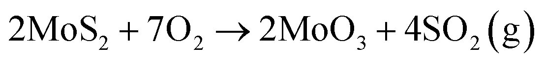 | (1) |
The products of such a reaction leave the MoS2 surface, which results in formation of triangular etch pits due to hexagonal surface symmetry.8,14,15 Most of the computational studies have been focused on the initial steps of defective or perfect MoS2 surface oxidation, namely, dissociation of O2 molecules, and adsorption of oxygen atoms and their complexes with S and/or Mo atoms, as well as formation of sulfur vacancies by the action of an attacking oxygen molecule.11,16,17 However, according to our knowledge, it has never been confirmed that at the atomic level, oxidative etching proceeds through eqn (1).
Herein, we report the surface presence of the sub-nm MoOx clusters in the oxidative etching of the MoS2 samples at 370 °C, where the Mo oxides start to form on the MoS2 surface. Through accurate AFM investigations together with density functional theory (DFT) simulations as well as local Raman spectroscopy, we discuss the origin, chemical composition and most probable conformations of the sub-nm MoOx clusters. Additional energy dispersive X-ray spectroscopy (EDS), wavelength dispersive X-ray spectroscopy (WDS), X-ray absorption near edge spectroscopy (XANES) and Kelvin probe AFM investigations agreed with the AFM and DFT findings.
Experimental
Laboratory grade 2H molybdenite crystals were bought from SPI Supplies, West Chester, PA, USA, catalogue number #429MM-AB. The MoS2 samples have been mechanically exfoliated using a standard blue tape and transferred on fine polished and basically undoped <111> Si crystals with a resistivity more than 10![[thin space (1/6-em)]](https://www.rsc.org/images/entities/char_2009.gif) 000 Ω cm, bought from ITME, Warsaw, Poland. Prior to a sample transfer, the Si substrates were ultrasonically cleaned in sequential steps with deionized water, acetone, ethanol and isopropanol for 10 min each. After each ultrasonication step, the substrate was dried with pure N2. At the end of ultrasonic cleaning, oxygen plasma (PE-25, Plasma Etch, 150 mTorr O2, 100 W RF power, 180 s) was used to get rid of any remaining residues/pollutants. Due to subsequent heating studies at temperatures of more than 350 °C, no annealing or any other cleaning methods have been used to remove any remaining traces of the blue tape from the Si substrates. After exfoliation, the samples were heated in air at 370 °C for 15 minutes on a standard hot plate covered with a quartz Petri dish to ensure a controlled atmosphere and proper distribution of temperatures within a heating zone. The hot plate was calibrated with a standard thermocouple and a Pt thermometer to yield a temperature error of ±2 °C on the sample surface. For cluster analysis, two separate samples were investigated. 1100+ clusters were selected from sample 1, and 350+ clusters were selected from sample 2.
000 Ω cm, bought from ITME, Warsaw, Poland. Prior to a sample transfer, the Si substrates were ultrasonically cleaned in sequential steps with deionized water, acetone, ethanol and isopropanol for 10 min each. After each ultrasonication step, the substrate was dried with pure N2. At the end of ultrasonic cleaning, oxygen plasma (PE-25, Plasma Etch, 150 mTorr O2, 100 W RF power, 180 s) was used to get rid of any remaining residues/pollutants. Due to subsequent heating studies at temperatures of more than 350 °C, no annealing or any other cleaning methods have been used to remove any remaining traces of the blue tape from the Si substrates. After exfoliation, the samples were heated in air at 370 °C for 15 minutes on a standard hot plate covered with a quartz Petri dish to ensure a controlled atmosphere and proper distribution of temperatures within a heating zone. The hot plate was calibrated with a standard thermocouple and a Pt thermometer to yield a temperature error of ±2 °C on the sample surface. For cluster analysis, two separate samples were investigated. 1100+ clusters were selected from sample 1, and 350+ clusters were selected from sample 2.
AFM measurements
A Cypher S AFM (Asylum Research, Goleta, CA, USA) in a contact mode in air and with an MLCT-F cantilever (Bruker, Santa Barbara, CA, USA) was utilized to perform scratching/removal of the MoO3 from the thermally oxidized MoS2 flakes. Each time, a specific area was scratched several times with a scanning rate between 2.60 and 4.88 Hz at loads between 0.6 ± 0.1 and 12 ± 1 nN. Loads were calibrated from a spring constant and sensitivity factors, which were obtained from thermal resonance of the used cantilever using routines available within the data acquisition software. The same AFM but in a light tapping mode in air was utilized for topography imaging of the sample before and after scratching. An AC160TS-R3 cantilever (Asylum Research) was used to collect high-resolution AFM images with at least 1536 points per line. All raw AFM data were treated with the Gwyddion software (v.2.51, Czech Metrology Institute, Brno, Czech Republic).18 Standard line-by-line first or second-order horizontal flattening together with removal of occasional glitches was applied. No other image treatment and/or conditioning were performed.DFT calculations
DFT calculations were performed on periodic slab models with the code VASP 6.2.19,20 Mo(4p, 4d, and 5s), S(3s and 3p) and O(2s and 2p) electrons were treated explicitly, and the interaction between the inner electrons and the nuclei was treated with the projector augmented wave method.21,22 The exchange-correlation functional proposed by Perdew, Burke and Ernzerhof (PBE)23 was adopted. The long-range dispersion was added to the potential according to the DFT+D3 scheme with a Becke–Johnson damping function.24,25 Thresholds of 10−5 eV and 0.01 eV Å−1 were adopted to truncate the electronic and ionic loops. A smearing of 0.05 eV was used to ensure convergency of the self-consistent field process. The lattice relaxation of the MoS2 monolayer was done with a mesh of 6 × 6 × 6 special k-points and a kinetic cutoff of 600 eV, yielding lattice parameters in good agreement with the experiment (a and b = 0.315 nm, and c = 1.207 nm). Static relaxations of (MoxOy)n/MoS2 structures were then performed at the Γ point with a cutoff of 400 eV. Spin-polarization effects were included in all calculations. Dipole and quadrupole corrections to the total energy were applied along the non-periodic direction for all calculations on slab models.26 In order to avoid spurious interactions between the replica of the slab models, a vacuum region of at least 1.5 nm was included along the non-periodic direction in the supercell. All calculations were carried out adopting a (5 × 2√3) MoS2 supercell. This box is large enough (1.58 nm × 1.09 nm) to simulate the formation of isolated mono- and dimer species. The (MoO3)ML/MoS2 interface is build superimposing a (4 × 3) supercell of MoO3 onto the aforementioned (5 × 2√3) MoS2 supercell. The residual strain arising from the lattice mismatch (0.2% and −1.3% along a and b) is released adapting MoO3 to the MoS2 lattice. The formation energy, Ef, has been calculated through the following equation: | (2) |
E(MoxOy/MoS2) is the total energy of an oxidized MoS2 supercell, which has one MoOx monomer or dimer. E(MoS2) is the total energy of a pure MoS2 supercell with or without a sulphur vacancy. μMo and μO are chemical potentials of Mo and O atoms, respectively.
The structures reported in the paper were obtained by static relaxations, starting from initial guess structures designed by chemical intuition. The choices to consider among all possible MoxOy species were the Mo1O2 and Mo1O3 monomers, as well as Mo2O4 and Mo2O6 dimers, as is discussed in the subsequent sections.
The height of the adsorbed MoxOy clusters was defined as the difference between the Z coordinate of the apical O atom of the cluster with respect to the average of the S atoms from the MoS2 basal plane.
Raman measurements
The Raman map was collected using a Horiba Jobin Yvon LabRAM HR800 Raman spectrometer. Measurements were made using a 532.0 nm laser excitation line with a 100× objective lens and a 1800 g mm−1 grating. The power was set below 5 mW to minimize any oxidative effects during Raman mapping. An area of 15 × 15 μm consisting of 30 × 30 points with a 0.5 μm step size was chosen for mapping. At each point, data in each spectral window were collected for 30 s. Two spectral windows at each point were taken.Kelvin-probe force microscopy (KPFM) measurements
A Cypher S AFM double-pass amplitude-modulated KPFM with ASYELEC-01 cantilevers (Asylum Research) was utilized. During the KPFM measurements, the bias voltage was applied to the tip, while the sample was ground. The raw, i.e., untreated KPFM tip-sample CPD data in volts (“Nap potential”) were analyzed with Gwyddion.18XANES measurements
The chemical state and local structure of MoS2 flakes on Si substrates were examined using X-ray absorption fine structure (XAFS) measurements. XAFS spectra were collected at the PEEM/XAS end station at the Solaris National Synchrotron Radiation Centre in Cracow, Poland. XAS beam parameters involved a photon energy range of 300–1600 eV with a relative energy resolution (ΔE/E) not worse than 0.00025, a beam size at the sample of 0.200 mm horizontally and 0.050 mm vertically and a photon flux at the sample of 109–1010 [ph/s/100 mA]. The sample was mounted on a standard nonmagnetic and conductive Elmitec PEEM sample holder for scanning electron microscopy (SEM)-EDS measurements.
The studies were performed with a scanning electron-ion microscope Crossbeam 540× (Zeiss) equipped with an EDS X-MAX detector (Oxford Instruments) with an active area of 80 mm2. An EDS spectrometer was calibrated for the Cu Kα line and controlled with a Smart SEM (ZEISS) and the Aztec 4.2 (Oxford Instruments) software. The surface morphology was imaged using an SESI and In-Lens detectors (mix signal) at an accelerating voltage of 5 kV, a working distance from the column WD = 5 mm and a stage tilt of 0°.
SEM-WDS measurements
A Cameca SX100 Electron Probe Microanalyzer (EPMA, manufactured at Courbevoie Cedex, France, 2000) equipped with 4 WDS detectors was used. Electrons were accelerated to 7.5 keV and regulated to a 10 nA beam current. The four WDS detectors were set to PC0-TAP-PET-LPET diffracting crystal configuration for point analysis to find O–Si–S–Mo concentrations on modified flakes. The position and reference intensities of O Ka were calibrated on a LiNbO3 crystal (Li: 4.6947 wt%, Nb: 62.8395 wt%, and O: 32.4658%). A molybdenite crystal (S: 40.06 wt%; Mo: 59.86 wt%) was used for referencing the positions and intensities of the S Kα and Mo Lα peaks. The Si Kα peak position and intensity were calibrated by using a silicon substrate as a reference sample. Counting times were set to 20 s on the peak and 10 s on single background position with a precise slope. Optimal single-background positions and precise slopes were graphically estimated using the HussariX software (https://github.com/sem-geologist/HussariX). X-ray intensities were calculated in wt% using the Cameca Peaksight 5.1 software with a built-in X-PHI matrix correction method in conjunction with the built-in database of Mass Attenuation Coefficients. To eliminate the sample charging, conductive contacts were made with the sample through a standard conductive carbon tape (SPM supplies).Results and discussion
Fig. 1 shows a high-resolution non-contact AFM topography image of a thick MoS2 flake which was heated at 370 °C for 15 minutes. Under such conditions, the basal MoS2 layer has been etched at a large portion of the flake. Simultaneously, underlying MoS2 layers have been incompletely etched. Etching resulted in formation of triangular etch pits of various depths, between one to seven MoS2 layers. In addition, some small and isolated spots are barely visible in Fig. 1(a). To investigate whether the spots are not AFM imaging artefacts, part of the image in Fig. 1(a) – marked by a dashed green box – was square rastered several times with an AFM tip.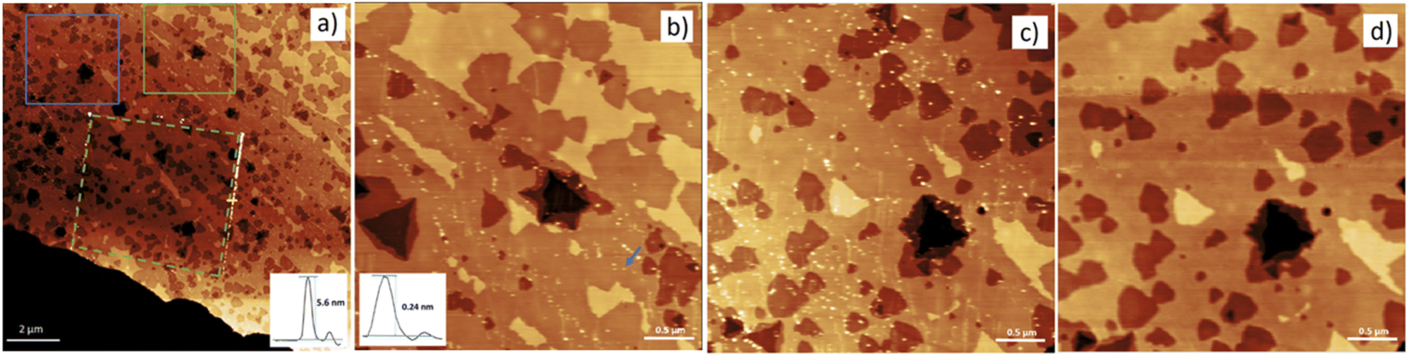 | ||
| Fig. 1 Non-contact AFM topography of a thermally etched MoS2 flake. (a) Image taken after rastering the area depicted by a dashed-green box. Inset: the height profile of piled-up debris along the yellow line. Image Z-scale 6.5 nm. (b) Magnified area from a solid-green box in (a). Inset: a typical cross-section along a single MoOx cluster marked by a blue arrow in (b). Image Z-scale 4.2 nm. (c and d) Magnified area depicted by a blue box in (a) before (c) and after (d) rastering the whole flake. Image Z-scale is 3.8 nm in (c) and 3.3 nm in (d). Brighter colors represent higher Z-values. | ||
As a result of rastering, a collection of white “debris” with a typical height of ca. 6 nm appeared at the border of the rastered zone. Thus, the etched surface was indeed covered with a considerable number of “particles”. To investigate these “particles” in greater detail, magnified AFM topographs of non-rastered zones are shown in Fig. 1(b) and (c). Therein, many clearly distinguishable and sub-nm thick clusters can be identified. An inset in Fig. 1(b) shows the typical height of such clusters to be only ca. 0.2 nm. These observations suggest that the “debris” discussed earlier originated from the piling up many of such sub-nm clusters.
Next, the sample was rastered in a contact mode to detect only loosely surface-bound clusters. Then, a high resolution non-contact AFM image of the same area was collected for further studies, see Fig. S1, ESI.† By comparing the topography before and after rastering, see Fig. 1(c) and (d), one concludes that AFM scratching displaced a great majority of sub-nm clusters without inducing any damage to the basal plane of the MoS2 flake. For further analyses, 1469 movable clusters from two separately prepared samples were randomly chosen, and their height profiles were obtained.
Fig. 2 shows a collective height histogram of the chosen clusters. The maximum height reading error in AFM experiments was only 0.03 nm. Therefore, a 0.05 nm bin size was chosen for the histogram. See Fig. S2–S4 in the ESI† regarding reproducibility of the results. A considerable portion of the clusters in Fig. 2 is shorter than the typical thickness of a single MoS2 layer, which is ca. 0.7 nm. This proves that movable clusters are not remainders of the non-etched MoS2. Next, Gaussian fits to the histogram were produced. Single Gaussian yielded one peak at 0.405 ± 0.020 nm. Double Gaussian produced two peaks at 0.236 ± 0.006 nm and 0.472 ± 0.021 nm. Both visually and via a χ2 test, the double Gaussian fit is much better than the single Gaussian, see Table S1, ESI.† Noteworthily, due to the large number of the data points within the histogram, its maxima are obtained with smaller errors than the AFM height reading errors for individual data points.
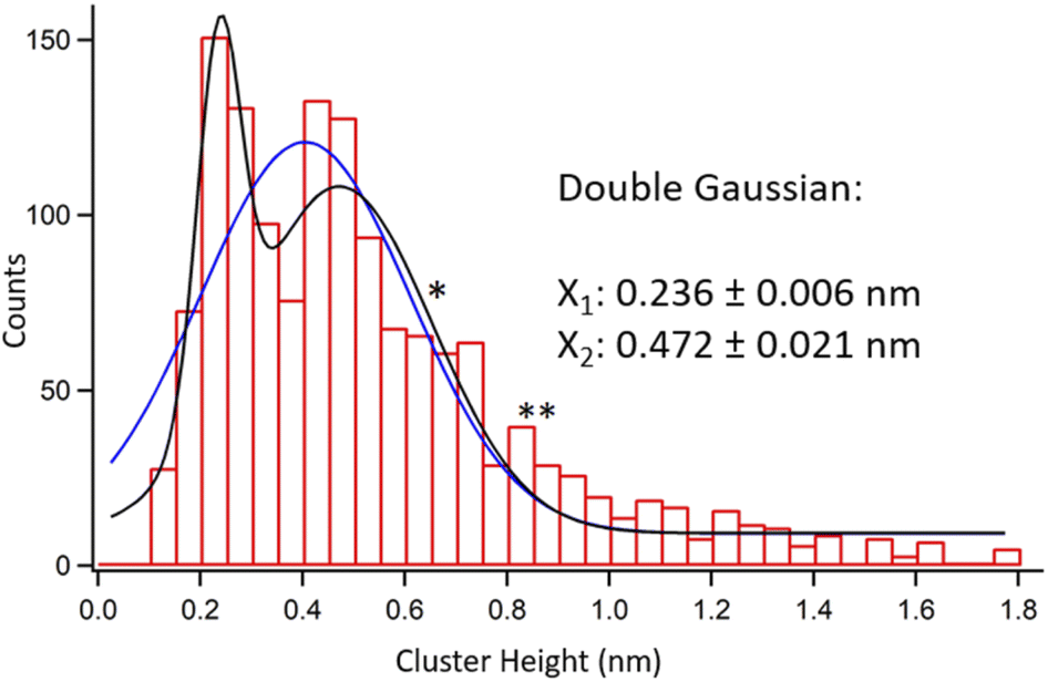 | ||
| Fig. 2 Height histogram of randomly chosen 1469 oxide clusters on two thermally etched MoS2 flakes. | ||
The clusters in Fig. 2 were either reabsorbed or originated from single etching events on the MoS2 samples. The latter means that they were produced and trapped at the same spots on the surface. More than 99% of the clusters were found exclusively within the etched regions, i.e., away from any intact MoS2 basal planes, see Fig. 1(a) and (b) as well as S2 in the ESI.† If such clusters detached and reabsorbed elsewhere, then they would appear also on the intact basal surface. Moreover, most of the reabsorbed species would locate at edges of the etched zones, which is also not the case here. Due to sub-nm heights of the obtained clusters and their exclusive presence only within the etched zones, we hypothesize that they are oxidation products caught in the act just after single etching events.
In order to elucidate the chemical composition of the clusters, DFT simulations were performed to investigate conformations taken by sub-nanometric MoxOy fragments onto the MoS2 monolayer. We did not aim at modelling the whole oxidation pathway, which is still unclear and has been the subject of several studies.2,11,12,17 Thus, we concentrated on the final outcomes of the oxidative events and classified them by topographic heights as well as thermodynamic stability of the resulting MoxOy species, see eqn (2). Four types of molybdenum oxide species were considered: Mo1O2 and Mo1O3 monomers and their dimers, i.e., Mo2O4 and Mo2O6. They agree with XPS and XAS experimental observations which show that MoO3 is the most expected oxide, and MoO2 could also be marginally present.2,27,28 Furthermore, out of all the Mo oxides, the MoO2 and MoO3 are thermodynamically preferred, and the MoO3 crystals are the most stable.29
In order to verify the role of point defects as active centers for oxidation, each MoxOy type was simulated onto three MoS2 surface spots: (i) stoichiometric MoS2, (ii) near single sulfur vacancy (SSV) and (iii) at the SSV. The cluster height above the MoS2 monolayer was calculated referring to its topmost atom and the average Z coordinate of the atoms from the top S layer in the dichalcogenide slab.
Fig. 3 presents our DFT simulation results. For the Mo1O2 molecule, in Fig. 1(a)–(c), the simulated heights changed from 0.299 nm on pristine MoS2 to 0.183 nm near the SSV and to 0.290 nm at the SSV. The structures near and at the SSV had comparable thermodynamic stability, while the structure on pristine MoS2 was the least stable. In the case of Mo1O3 monomers, Fig. 1(d)–(f), more stable species were obtained compared to Mo1O2. Their simulated heights changed from 0.292 nm on pristine MoS2 to 0.261 nm near the SSV and 0.243 nm at the SSV. The Mo1O3 structure at the sulfur vacancy was the most stable and matched very well with our experimental results.
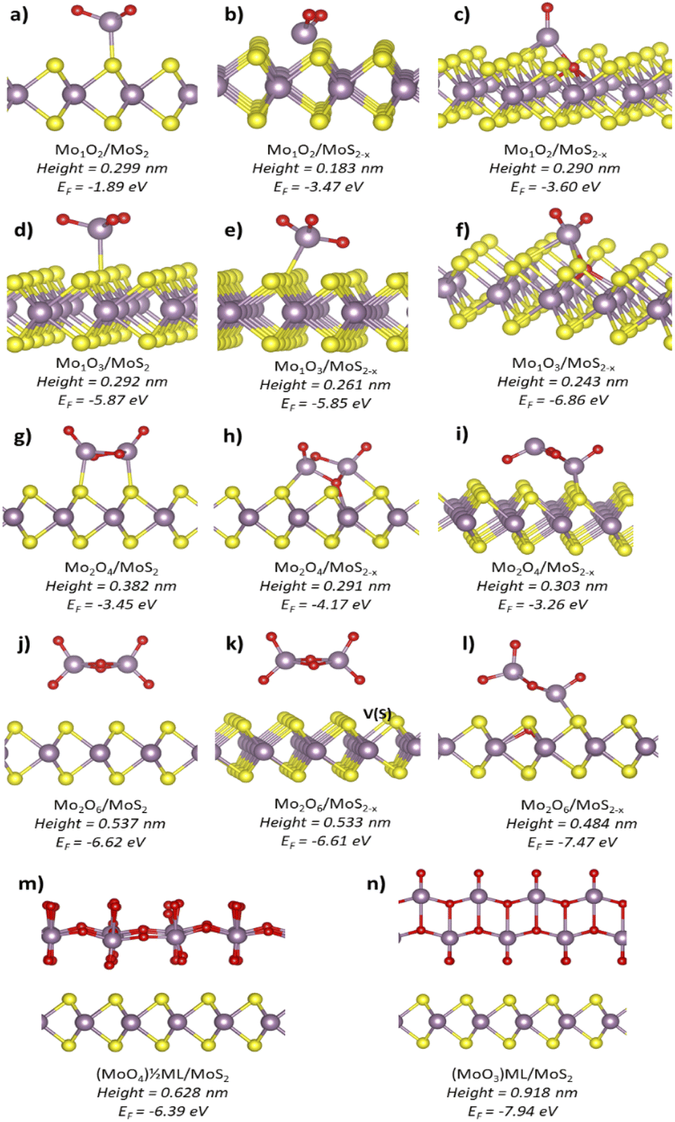 | ||
| Fig. 3 Side views of DFT structures along with their expected heights and formation energies (EF) per considered MoxOy unit. (a, d, g and j) MoxOy species on stoichiometric MoS2. (b, e, h and k) MoxOy species adsorbed near the SSV. (c, f, i and l) MoxOy species adsorbed at the SSV. (m and n) Continuous MoO3 structures: the half-monolayer and full monolayer, respectively. | ||
A remarkable increase in height was reported when the dimers were considered. For Mo2O4, the height varied from 0.382 nm on stoichiometric MoS2 to 0.291–0.303 nm on defective MoS2. The Mo2O6 species positioned themselves at larger distances from the MoS2 surface than Mo2O4 dimers. Such distances decreased from 0.537 nm on a pristine sample to 0.533 nm near the SSV and 0.484 nm at the SSV. The last structure, shown in Fig. 3(l), resulted from spontaneous reorganization of the Mo2O6 cluster at the SSV. During such a process, the cluster lost an O atom, which filled the S vacancy. The resulting structure was the most stable out of all considered dimers. The curious feature of complete detachment of an O atom from the cluster has been double-checked. Despite several attempts, it was not possible to identify a stable structure with the O atom entering the S vacancy and the Mo2O6 molecule remaining intact. Interestingly, similarly to the case of monomers, the (MoO3)n species being more stable than the corresponding (MoO2)n species.
Formation of continuous MoOx layers was also simulated. Fig. 3(m) shows a half monolayer formed by single MoO6 octahedra with a resulting stoichiometry of MoO4 and a height of 0.628 nm above MoS2. Fig. 3(n) shows a full α-MoO3 monolayer with two stacked planes of MoO6 octahedra and a height of 0.918 nm above MoS2. For comparison, the height of a single MoS2 layer was 0.60 nm at a coherent level of calculations.
Comparing the heights obtained by simulations with the results of the AFM measurements, the most prominent type of the clusters in Fig. 2 corresponds to the MoO3 monomer at the SSV. Its simulated height of 0.243 ± 0.001 nm matches extremely well with 0.236 ± 0.006 nm observed in the experiments. The simulated structure of the MoO3 species where a Mo atom is extracted from the MoS2 surface is also provided, see Fig. S5 in the ESI.† Such a structure was coordinated by three oxygen atoms and showed the height of 0.222 nm, which is still close to the first peak in Fig. 2. Other types of MoO3 adsorption modes yielded substantially different heights. Such a spectacular agreement between the experimental AFM height data and simulated heights of the expected clusters seems truly significant. It strongly points towards single MoO3 molecules produced on the MoS2 surface predominantly at sulfur vacancies during its oxidative etching.
It has been already shown that during oxidative etching, atmospheric oxygen reacts with a MoS2 basal plane at defect sites to produce volatile oxide compounds. Two kinds of molecular mechanisms were proposed, i.e., either etching along the zig–zag (ZZ)-Mo or ZZ-S edges.8,15 Exclusive presence of the MoO3 molecules within the single sulfur vacancies is strong proof for such mechanistic assumptions since it confirms the stoichiometry of eqn (1) and shows the MoO3 caught on the surface just before leaving it.
Next, we discuss the second peak in the height histogram. Its best match from simulations is the MoO3 dimer at the SSV, which also is the most stable out of all the considered dimers. To ponder on a role of sulfur vacancies in more detail, we calculated the formation energies of dimers aggregating from two MoO3 monomers adsorbed separately, see Table S2 in the ESI.† We obtained an energy gain of 0.69 eV if the dimers aggregated at the SSV compared to aggregation on a pristine surface. This suggests that SSVs act as nucleation centers both for monomers and dimers.
The second histogram peak in Fig. 2 is lower in amplitude and much wider than the first peak. Its lower amplitude relates to lower likelihood of obtaining a MoO3 dimer vs. monomer at the reaction spot. The width of the second peak might as well relate to other chemical forms of the MoO3 expected on the surface. For example, a single star (*) marks the height associated with half of the MoO3 layer. This structure is presented in Fig. 3(m) and is also known as a metastable monoclinic β-MoO3 structure.29 A similar height is also expected from thermodynamically favored chain-like structures of the MoO6 octahedra, a.k.a molybdenum polyoxides.30 Two stars (**) in Fig. 2 mark the expected height of fully formed fragments of the most stable α-MoO3 monolayer, see Fig. 3(n).
To further report the MoO3 stoichiometry of the clusters, we performed a detailed Raman analysis. We concentrated on comparisons between the high quality Raman spectra collected around the border between rastered (without oxide) and unrastered (with oxide clusters) MoS2 surfaces. We extracted such data from the Raman map, see the ESI.†Fig. 4(a) and (b) show the optical and topography images of the selected area. Fig. 4(c)–(e) display the Raman spectra taken along a dashed line from Fig. 4(a). Such a line originates within a rastered zone, passes through a border region and ends up in an unrastered zone. Similarly, the Raman spectra displayed in Fig. 4(d) and (e) are arranged from the ones collected on unrastered zone (on top) towards the ones collected on the rastered zone (on the bottom).
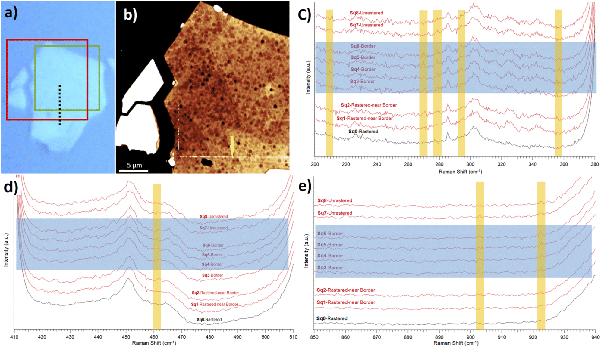 | ||
| Fig. 4 Raman and AFM studies on a selected MoS2 flake. (a) Optical image of the investigated flake. A green box shows the rastered region. (b) NC-AFM topography image (6.2 nm Z-scale) of an area depicted by a red box in (a). Brighter colors represent a higher Z-scale. A yellow arrow shows a border between rastered and unrastered zones, where Mo oxide clusters are piled up. The scale bar is 5 μm. (c–e) Raman spectra obtained from the flake along the dashed black line in (a). Blue rectangles show the border area in the overlaid spectra, and yellow windows mark Raman shifts with noticeable changes between rastered and border zones. | ||
While it is difficult to claim any presence of typical Raman peaks associated with the MoO3 oxide, the data in Fig. 4 show differences between rastered and unrastered zones in the case of several particular Raman shifts. For example, there is a clear difference between border and rastered regions at around the 278 cm−1 Raman shift in Fig. 4(c). Namely, the peaks from within the MoO3 containing zone in the first six spectra (from top) collected in unrastered and border regions are absent in the last two Raman spectra collected in the MoO3 depleted zone. Similar observations can be extended to other Raman shifts associated in the literature, see Table 1, with the presence of MoO3 and MoO3−x. Often, the differences are not striking, which confirms difficulties associated with collecting Raman spectra of (sub) monolayers. Till now – at least according to our knowledge – obtaining the Raman signature of thin MoO3 layers onto MoS2 flakes has not been reported. At best, some authors were able to report Raman shifts only for fully established MoO3 crystals on Si substrates.2
| Raman shift (cm−1) | Peak attribution | Raman shifts observed in the literature (cm−1) |
|---|---|---|
| 210 | Ag-δ(OMo2) in MoO3 (ref. 31 and 38) | 211,38 218,31 and 21739 |
| 270 | B2uδ(O![[double bond, length as m-dash]](https://www.rsc.org/images/entities/char_e001.gif) Mo) in MoO3 (ref. 31 and 40) Mo) in MoO3 (ref. 31 and 40) |
270 and31 267 (calculation)40 |
| 278 | B1u-δ(OMo) in MoO3 (ref. 31 and 40) and MoO3−x (ref. 38) |
280, 282,38 270,31 and 276 (calculation)40 |
| 294 | B3gδ(OMo) in MoO3 (ref. 31 and 40) |
293,38,41 291,31,39 and 290 (calculation)40 |
| 356–359 | B3uδ(OMo) in MoO3 (ref. 31 and 40) and MoO3−x (ref. 38) |
356,38 358,31 and 358 (calculation)40 |
| 461 | B1g-ν(OMoO3) in MoO3−x (ref. 38) | 46238 and 46142,43 |
| 903 | β-MoO3 (ref. 44 and 45) m-MoO3 (ref. 31) | 90231,44–46 |
| α-MoO3 within MoO3−x (ref. 46) | ||
| 922–923 |
Ѵ(OMo) in α-MoO3 hydrides31,47 and hydrates48 |
922,31,49 923,47 and 92048 |
| Mo–O2 mode in MoO3−x quantum dots49 |
As mentioned earlier, we did not observe any noticeable differences in the Raman spectra between rastered and unrastered regions around 666, 821, and 996 cm−1, which are associated with pure MoO3.10,31,32 The 666 cm−1 mode is assigned to the triply coordinated oxygen stretching mode, ν(OMo3),31,33 which is specific to a full α-MoO3 monolayer. This is not the case here, since even our border region consists of randomly oriented but yet separated MoO3/MoO3−x clusters. Raman peaks at 821 and 996 cm−1 come from a double-coordinated oxygen stretching mode, ν(OMo2), and a terminal oxygen stretching mode, ν(OMo), respectively. However, a weak MoS2 peak at around 820 cm−1 (second order Raman mode of A1g in MoS2)34–36 and a broad silicon peak between 930 and 1000 cm−1 (second order Raman scattering of Si)37 effectively mask them.
Overall, Raman spectroscopy produced evidence for the surface presence of the MoO3 stoichiometries in the unrastered and border regions, i.e., the ones containing the AFM-detected clusters.
To shed more light in the presence of MoO3 clusters within the unrastered and border zones, we performed the KPFM study. Fig. 5 shows the topography and corresponding contact potential difference (CPD) for an area around the border between rastered and unrastered regions of the MoS2 flake from Fig. 4(b). Sub-nm white spots in the unrastered region are well visible – as single white dots – at the right side of the topography image in Fig. 5(a). The 5 mV (on average) difference in the CPD values between unrastered vs. rastered zones, see Fig. 5(c), yields the same difference in the work function (WF). The border region, where Mo oxide clusters were piled up show even higher values of the WF. Qualitatively, the same trends were observed in other studies. In particular, Zhang et al.50 found out that a homogeneous 6 nm MoO3 layer atop of a MoS2 flake showed a 260 mV higher WF than pure MoS2. Rogala et al.27 showed that a continuous 2 nm MoO3/MoOx layer atop of a MoS2 flake resulted in a 70 to 100 mV higher WF than pure MoS2. Following this trend, very small WF differences are expected between the MoS2 surface and isolated MoO3/MoOx clusters covering it only sparsely. However, while the thickness of the piled-up Mo oxides at the border is between 4 and 15 nm, it showed only about a 25 mV higher WF than on rastered MoS2. We expect that such a low WF difference is due to the inhomogeneity and small width of the border area. The latter produces only a small contribution to the overall KPFM signal, which is collected mostly from the MoS2 surface.
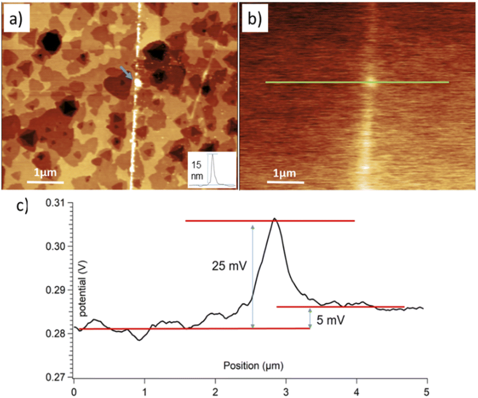 | ||
| Fig. 5 (a) Topography (4.9 nm Z-scale) and (b) contact potential difference, CPD, (0.047 V Z-scale) for an area around the border between rastered (left) and unrastered (right) regions of the flake depicted in Fig. S8.† The inset in (a) shows the height profile along the border marked by a blue arrow. (c) Cross-section taken along a green line in (b). Notably different CPD values are noticed in each of the regions, i.e., rastered, border, and unrastered. | ||
In conclusion, while the KPFM did not produce a direct chemical identification of the scanned species, we observed differences between MoO3 rich and lacking zones, which agreed with some previously published results.
To elucidate coordination of the oxidation products in more detail, an untreated (as-exfoliated) and thermally etched/oxidized flakes were chosen for XANES measurements. Fig. 6 shows the comparative XANES spectra. Mo M2 and M3-edges in an unmodified MoS2 flake produced two peaks at 413.5 eV and 396.4 eV, respectively. In comparison to the untreated sample, the XANES spectra of an etched/oxidized flake shows a 0.5 eV blue shift of the Mo M2 edge and a new M3 post peak at 399.8 eV. These two important features of the Mo M2 and M3 edges have been attributed to the presence of MoO3 by Rogala et al.27 Moreover, there is a strong peak at 531.5 eV in the XANES spectra of a modified flake which is absent in the case of the untreated sample. Lajaunie et al.51 studied the XANES spectra of the oxygen K-edges in MoO2 and MoO3. They found out that oxygen in MoO3 produced a strong peak at 531.2 eV, while the strongest peak of the O K-edge in MoO2 was at 534.5 eV. Based on these data, the peak at 531.5 eV in our XANES spectra of the modified flake shows that the oxidation products are MoO3 rather than MoO2.
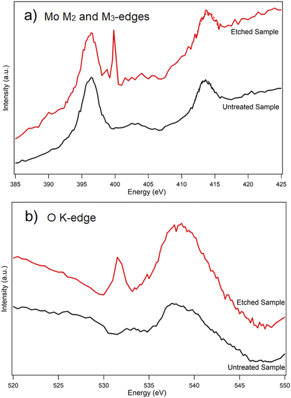 | ||
| Fig. 6 XANES spectra of (a) an untreated MoS2 flake and (b) a modified MoS2 flake heated at 370 °C in air. | ||
Finally, additional SEM-EDS and SEM-WDS studies presented in the ESI† show that the presence of isolated and sparsely present sub-nm MoOx clusters produced a detectable increase in the O/Mo ratio on investigated MoS2 flakes.
Conclusions
Thermal etching of a single MoS2 flake at 370 °C produced not only etch pits, but also some sub-nm oxide clusters. The high resolution AFM data together with DFT simulations show that majority of the clusters were MoO3 monomers and dimers caught in the act of being produced at the single sulfur vacancies. Raman spectroscopy confirmed the surface presence of the MoO3 stoichiometry. The KPFM and SEM-EDS/WDS data strengthened this hypothesis, although were not able to directly differentiate the MoO3 clusters from an underlying MoS2 surface. The XANES results contributed to confirming the MoO3 stoichiometries present on the MoS2 surface. Our findings confirm that during MoS2 thermal oxidative etching, Mo atoms leave the surface mainly as MoO3 molecules rather than any other forms of Mo oxides. This confirms the stoichiometry of the thermal etching process exemplified in eqn (1). Moreover, sulfur vacancies were suggested by our DFT results to act as nucleation sites for the thermally induced oxidative etching.Beyond fundamental research, these findings are expected to find applications in nanoscale catalysis, since defected MoS2 as well as MoO3 clusters are potent catalysts for numerous important reactions including the hydrogen evolution reaction and oxygen reduction reaction.
Conflicts of interest
There are no conflicts to declare.Acknowledgements
The work of SS and RS was supported by the National Science Center, Poland, grant no. 2017/27/B/ST4/00697. We acknowledge Dr Agata Królikowska for help with Raman measurements. We thank Dr Tomasz Giela, Dr Ewa Madej, Dr Anna Mandziak and Dr Marcin Zając from the SOLARIS National Synchrotron Radiation Centre in Cracow, Poland, for help with XANES measurements. We thank Dr Sylwia Turczyniak-Surdacka for SEM-EDS measurements. We thank Dr Petras Jokubauskas for SEM-WDS measurements.References
- Q. H. Wang, K. Kalantar-Zadeh, A. Kis, J. N. Coleman and M. S. Strano, Nat. Nanotechnol., 2012, 7, 699–712 CrossRef CAS PubMed.
- R. Szoszkiewicz, Mater, 2021, 14, 5979 CrossRef CAS PubMed.
- K. Kang, S. Xie, L. Huang, Y. Han, P. Y. Huang, K. F. Mak, C. J. Kim, D. Muller and J. Park, Nature, 2015, 520, 656–660 CrossRef CAS.
- Y. Wang, M. Mayyas, J. Yang, J. Tang, M. B. Ghasemian, J. Han, A. Elbourne, T. Daeneke, R. B. Kaner and K. Kalantar-Zadeh, Adv. Funct. Mater., 2021, 31, 2005866 CrossRef CAS.
- J. Shim, S. H. Bae, W. Kong, D. Lee, K. Qiao, D. Nezich, Y. J. Park, R. Zhao, S. Sundaram, X. Li, H. Yeon, C. Choi, H. Kum, R. Yue, G. Zhou, Y. Ou, K. Lee, J. Moodera, X. Zhao, J. H. Ahn, C. Hinkle, A. Ougazzaden and J. Kim, Science, 2018, 362, 665 CrossRef CAS PubMed.
- K. Kang, K. H. Lee, Y. Han, H. Gao, S. Xie, D. A. Muller and J. Park, Nature, 2017, 550, 229–233 CrossRef.
- E. Yalon, C. J. McClellan, K. K. H. Smithe, M. Muñoz Rojo, R. L. Xu, S. V. Suryavanshi, A. J. Gabourie, C. M. Neumann, F. Xiong, A. B. Farimani and E. Pop, Nano Lett., 2017, 17, 3429–3433 CrossRef CAS PubMed.
- H. Zhou, F. Yu, Y. Liu, X. Zou, C. Cong, C. Qiu, T. Yu, Z. Yan, X. Shen, L. Sun, B. I. Yakobson and J. M. Tour, Nano Res., 2013, 6, 703–711 CrossRef CAS.
- J. Wu, H. Li, Z. Yin, H. Li, J. Liu, X. Cao, Q. Zhang and H. Zhang, Small, 2013, 9, 3314–3319 CAS.
- M. Yamamoto, T. L. Einstein, M. S. Fuhrer and W. G. Cullen, J. Phys. Chem. C, 2013, 117, 25643–25649 CrossRef CAS.
- L. M. Farigliano, P. A. Paredes-Olivera and E. M. Patrito, J. Phys. Chem. C, 2020, 124, 13177–13186 CrossRef CAS.
- J. Martincová, M. Otyepka and P. Lazar, Chem. – A Eur. J., 2017, 23, 13233–13239 CrossRef PubMed.
- F. Jia, C. Liu, B. Yang and S. Song, Appl. Surf. Sci., 2018, 462, 471–479 CrossRef CAS.
- D. Lv, H. Wang, D. Zhu, J. Lin, G. Yin, F. Lin, Z. Zhang and C. Jin, Sci. Bull., 2017, 62, 846–851 CrossRef CAS.
- U. Ukegbu and R. Szoszkiewicz, J. Phys. Chem. C, 2019, 123, 22123–22129 CrossRef CAS.
- S. Kc, R. C. Longo, R. M. Wallace and K. Cho, J. Appl. Phys., 2015, 117, 135301 CrossRef.
- J. Pető, T. Ollár, P. Vancsó, Z. I. Popov, G. Z. Magda, G. Dobrik, C. Hwang, P. B. Sorokin and L. Tapasztó, Nat. Chem., 2018, 10, 1246–1251 CrossRef.
- D. Nečas and P. Klapetek, Cent. Eur. J. Phys., 2012, 10, 181–188 Search PubMed.
- G. Kresse and J. Hafner, Phys. Rev. B: Condens. Matter Mater. Phys., 1993, 47, 558–561 CrossRef CAS PubMed.
- G. Kresse and J. Furthmüller, Comput. Mater. Sci., 1996, 6, 15–50 CrossRef CAS.
- P. E. Blöchl, Phys. Rev. B: Condens. Matter Mater. Phys., 1994, 50, 17953–17979 CrossRef.
- G. Kresse and D. Joubert, Phys. Rev. B: Condens. Matter Mater. Phys., 1999, 59, 1758–1775 CrossRef CAS.
- J. P. Perdew, K. Burke and M. Ernzerhof, Phys. Rev. Lett., 1996, 77, 3865–3868 CrossRef CAS PubMed.
- S. Grimme, J. Antony, S. Ehrlich and H. Krieg, J. Chem. Phys., 2010, 132, 154104 CrossRef PubMed.
- S. Grimme, S. Ehrlich and L. Goerigk, J. Comput. Chem., 2011, 32, 1456–1465 CrossRef CAS PubMed.
- J. Neugebauer and M. Scheffler, Phys. Rev. B: Condens. Matter Mater. Phys., 1992, 46, 16067–16080 CrossRef CAS PubMed.
- M. Rogala, S. Sokołowski, U. Ukegbu, A. Mierzwa and R. Szoszkiewicz, Adv. Mater. Interfaces, 2021, 8, 2100328 CrossRef CAS.
- S. Park, A. T. Garcia-Esparza, H. Abroshan, B. Abraham, J. Vinson, A. Gallo, D. Nordlund, J. Park, T. R. Kim, L. Vallez, R. Alonso-Mori, D. Sokaras and X. Zheng, Adv. Sci., 2021, 8, 2002768 CrossRef CAS.
- I. Alves de Castro, R. Shankar Datta, J. Zhen Ou, A. Castellanos-Gomez, S. Sriram, T. Daeneke, K. Kalantar-zadeh, I. A. de Castro, R. S. Datta, J. Z. Ou, S. Sriram, T. Daeneke, K. Kalantar-zadeh and A. Castellanos-Gomez, Adv. Mater., 2017, 29, 1701619 CrossRef.
- T. N. Walter, F. Kwok, H. Simchi, H. M. Aldosari and S. E. Mohney, J. Vac. Sci. Technol., B: Nanotechnol. Microelectron.: Mater., Process., Meas., Phenom., 2017, 35, 021203 Search PubMed.
- L. Seguin, M. Figlarz, R. Cavagnat and J. C. Lassègues, Spectrochim. Acta, Part A, 1995, 51, 1323–1344 CrossRef.
- M. R. Rahmani Taji Boyuk, S. Sovizi, H. Ghanbari, A. Simchi and N. Aboudzadeh, Ceram. Int., 2018, 44, 15795–15803 CrossRef CAS.
- J. Z. Ou, J. L. Campbell, D. Yao, W. Wlodarski and K. Kalantar-Zadeh, J. Phys. Chem. C, 2011, 115, 10757–10763 CrossRef CAS.
- V. S. Bagaev, V. S. Krivobok, S. N. Nikolaev, M. A. Chernopitssky and K. A. Savin, J. Russ. Laser Res., 2019, 40, 269–273 CrossRef CAS.
- B. C. Windom, W. G. Sawyer and D. W. Hahn, Tribol. Lett., 2011, 42, 301–310 CrossRef CAS.
- J. M. Chen and C. S. Wang, Solid State Commun., 1974, 14, 857–860 CrossRef CAS.
- J. H. Parker, D. W. Feldman and M. Ashkin, Phys. Rev., 1967, 155, 712 CrossRef CAS.
- M. A. Camacho-López, L. Escobar-Alarcón, M. Picquart, R. Arroyo, G. Córdoba and E. Haro-Poniatowski, Opt. Mater., 2011, 33, 480–484 CrossRef.
- K. Eda, J. Solid State Chem., 1992, 98, 350–357 CrossRef CAS.
- M. A. Py and K. Maschke, Phys. B+C, 1981, 105, 370–374 CrossRef CAS.
- P. A. Spevack and N. S. Mcintyre, J. Phys. Chem., 1992, 96, 9029–9035 CrossRef CAS.
- B. B. Wang, X. X. Zhong, R. W. Shao, Y. A. Chen, U. Cvelbar and K. Ostrikov, J. Phys. D. Appl. Phys., 2020, 53, 415109 CrossRef CAS.
- Y. Li, X. Chen, M. Zhang, Y. Zhu, W. Ren, Z. Mei, M. Gu and F. Pan, Catal. Sci. Technol., 2019, 9, 803–810 RSC.
- D. Liu, W. W. Lei, J. Hao, D. D. Liu, B. B. Liu, X. Wang, X. H. Chen, Q. L. Cui, G. T. Zou, J. Liu and S. Jiang, J. Appl. Phys., 2009, 105, 023513 CrossRef.
- N. Illyaskutty, S. Sreedhar, G. Sanal Kumar, H. Kohler, M. Schwotzer, C. Natzeck and V. P. M. Pillai, Nanoscale, 2014, 6, 13882–13894 RSC.
- A. M. Hashem, S. M. Abbas, A. E. Abdel-Ghany, A. E. Eid, A. A. Abdel-Khalek, S. Indris, H. Ehrenberg, A. Mauger and C. M. Julien, J. Alloys Compd., 2016, 686, 744–752 CrossRef CAS.
- D. Liu, W. Lei, X. Chen, J. Hao, Y. Jin, Q. Cui and G. Zou, J. Phys. Chem. B, 2009, 113, 16479–16482 CrossRef CAS PubMed.
- Y. Wang, M. Mayyas, J. Yang, M. B. Ghasemian, J. Tang, M. Mousavi, J. Han, M. Ahmed, M. Baharfar, G. Mao, Y. Yao, D. Esrafilzadeh, D. Cortie and K. Kalantar-Zadeh, ACS Appl. Mater. Interfaces, 2021, 13, 53181–53193 CrossRef CAS PubMed.
- D. Ding, W. Huang, C. Song, M. Yan, C. Guo and S. Liu, Chem. Commun., 2017, 53, 6744–6747 RSC.
- R. Zhang, X. Ma, C. An, D. Zhang, D. Sun, X. Hu and J. Liu, 2D Mater., 2019, 6, 035033 CrossRef CAS.
- L. Lajaunie, F. Boucher, R. Dessapt and P. Moreau, Ultramicroscopy, 2015, 149, 1 CrossRef CAS PubMed.
Footnote |
| † Electronic supplementary information (ESI) available: Topography images of the samples, separate height histograms of the samples, discussion of fitting parameters, additional DFT simulations, more details on Raman maps, and additional SEM-EDS and SEM-WDS investigations. See https://doi.org/10.1039/d2na00374k |
| This journal is © The Royal Society of Chemistry 2022 |