
 Open Access Article
 This Open Access Article is licensed under a Creative Commons Attribution-Non Commercial 3.0 Unported Licence
Feather-like few-layer WSe2 nanosheets grown on W substrates: an excellent electrocatalyst for the hydrogen evolution reaction
Yubao
Li
 *,
Linjing
Zhang
,
Jingchao
Xiao
and
Wei
Zhang
*
*,
Linjing
Zhang
,
Jingchao
Xiao
and
Wei
Zhang
*
College of Physics Science and Technology, Hebei University, Baoding 071002, China. E-mail: liyubao@hbu.edu.cn; zhangw@hbu.edu.cn
First published on 24th June 2022
Abstract
Thin films of few-layer WS2 nanosheets and WSe2 nanosheets were directly grown on W substrates via a scalable infrared-heating CVD method. The WSe2 nanosheets are in a unique feather-like assembly, and mainly composed of the 2H phase, while the presence of a metallic 1T phase was confirmed through atomic resolution TEM observation. Feather-like WSe2 nanosheets delivered excellent electrocatalytic performances for the HER in acid, including a low overpotential of 141 mV to yield a current at 10 mA cm−2, and superb long-term stability at high currents. The highly efficient electrocatalysis is mainly attributed to the unique feather-like morphology of the WSe2 nanosheets with numerous sharp barbules to help maximize the exposed edge sites, along with other beneficial factors including the presence of a 1T phase and slight O-doping.
Introduction
Generating hydrogen via water splitting has aroused intensive research interest to help alleviate current serious global pollution. However, the most efficient and best performing catalysts for the hydrogen evolution reaction (HER) are still costly noble metals such as Pt, which has severely hindered mass production due to cost concerns. Thus, researchers have been diligently looking for suitable nonprecious metal catalysts.1–3 Nanostructured catalysts of transition metal dichalcogenides (TMDs) are promising due to their high efficiency and good stability.1,4 It has been widely agreed that the electrocatalytic efficiency of TMD catalysts strongly relies on the number of active edge sites,5 but the basal planes of these 2-dimensional (2D) materials could also play significant roles if there was good electronic coupling between the substrate and the nanosheets.6 To fairly evaluate the catalytic performance of HER catalysts, the overpotential versus the reversible hydrogen electrode (RHE) required to generate a current at a density of 10 mA cm−2 has been generally accepted as a benchmarking metric, and for convenience herein we define it as η10 (the lower, the better).7 So far, both nanostructured TMD powder catalysts and thin film catalysts have been developed, and efforts have been focused on how to maximize exposed active edge sites and/or to form a low resistance contact, in a strong attempt to push TMD catalysts to reach their full potentials.A low η10 of 140 mV was realized on a powder catalyst of single-layer MoSSe nanodots, which was attributed to its high-percentage metallic 1T phase, high-density edge sites, the alloying effect and Se vacancies.8 Recently, a powder catalyst of mesoporous graphene-supported 2H-WS2 curved nanosheets reached an even lower η10, ranging between 117 and 142 mV, by tuning the layer number, strain, and S vacancies.9 WSe2, a star 2D-semiconductor among TMD family members for building novel electronic or photoelectric devices, was previously disclosed for its promising HER catalytic potential, with a η10 close to 240 mV being demonstrated for the powder catalysts of nanostructured WSe2 assembled on various carbons, including carbon fibre, graphene nanosheets, and carbon nanotubes.10–12 Recently, a η10 of 163 mV was reported for the powder catalyst of monolayer 1T phase WSe2 nanosheets supported on Ag2Se nanoparticles,13 and a η10 of 150 mV was realized by the powder catalyst of oxidized WSe2 nanosheets,14 demonstrating great potential of a WSe2-based electrocatalyst. The powder assembly of the above-mentioned TMD nanocatalysts might hinder their scale-up ink-casting application due to the technical concern over maintaining the distribution uniformity, the properties of the supporting material, and the Nafion loading, among other factors. Therefore, the synthesis of a thin film TMD electrocatalyst has been well pursued. In 2014, a η10 of 350 mV was reported for a WSe2 platelet thin film catalyst formed on a W substrate,15 which was worse than the above-mentioned best ones achieved on powder WSe2 catalysts and thin film MoS2 catalysts (with η10 ranging from 230–280 mV).16,17
We previously demonstrated outstanding HER catalytic activities for an uncapped WS2 nanotube array thin film (η10 = 156 mV) synthesized by a scalable infrared-heating CVD method.18 In this article, we report the direct large-area growth of few-layer WS2 or WSe2 nanosheets on W foil substrates using a similar CVD process, and their superior performances as an HER electrocatalyst. Specially, the feather-like WSe2 nanosheet thin film electrocatalyst, possessing lots of sharp barbules to boost active edge sites and containing both a semiconducting 2H phase and metallic 1T phase to help charge transfer, is capable of highly efficient catalysis for the HER in acid, with a low η10 of 141 mV and superb high-current stability over a long period of time, outperforming other TMD thin film electrocatalysts.
Experimental section
Nanomaterial synthesis
The nanomaterial films were grown via an infrared-heating CVD method, similar to that used in our earlier work.18 As shown in Fig. 1a, an infrared lamp (25 mm in light-beam size) was used as the heating source, a piece of tungsten foil (25 mm × 25 mm × 0.1 mm) was used as the heating target, the substrate was laid under the target foil at about 1 mm distance, and 0.5 g S or Se powders were placed in a quartz chamber (8 cm to the substrate edge). In a typical run, another piece of W foil (20 mm × 20 mm) was used as the substrate. First, the quartz tube reaction chamber was pumped down to a base pressure of 1 Torr, and then the pump was stopped to seal residual air in the reactor to serve as the oxygen source. The top surface of the W foil target was rapidly heated up to 850–900 °C with the high-power infrared light being turned on, and within a short period of time the temperature of the substrate was increased to 600–650 °C and that of the S/Se powders to 250–300 °C. Aftercontinuous growth for 25 min, the infrared lamp was turned off, and in the meantime, the reaction chamber was pumped down, leaving the sample under vacuum to cool down. After the CVD growth was finished, the top surface of the W substrate was entirely covered with a thick grey film.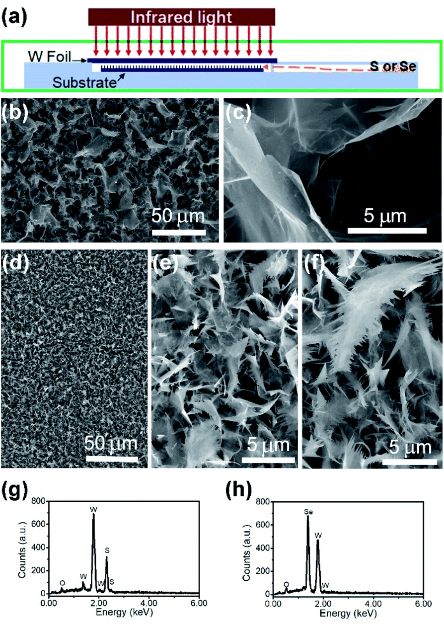 | ||
| Fig. 1 (a) Schematic diagram of the infrared-heating CVD setup. (b) and (c) SEM images of the film grown with S. (d)–(f) SEM images of film grown with Se. (g) EDS spectrum of the film grown with S. (h) EDS spectrum of the film grown with Se. | ||
Materials characterization studies
A field-emission scanning electron microscope (SEM, FEI Nova NanoSEM 450) was used to observe the morphology of the nanostructure films. X-ray diffraction (XRD) spectra of the nanostructures were recorded on a Bruker D8-Advance X-ray diffractometer with standard Cu Kα radiation. Raman spectra were obtained by using a Horiba Jobin Yvon LabRAM HR-Evolution Raman system with 532 nm laser excitation at room temperature. X-ray photoelectron spectroscopy (XPS, Thermo Scientific Escalab 250Xi) was carried out using a monochromatic Al Kα X-ray source (1486.6 eV), and all binding energies were referenced to that of a neutral C 1s peak. The detailed structures were further characterized via high-resolution transmission electron microscopes (TEM, JEM-ARM200F or JEM-2100F) operated at 200 kV. Energy-dispersive X-ray spectroscopy (EDS) coupled with SEM or TEM was employed to analyse the chemical compositions of the nanostructures.Electrochemical HER measurements
HER electrocatalysis measurements were carried out on a 3-electrode electrochemical workstation (CHI 760E) in an electrolyte of high-purity H2-saturated 0.5 M H2SO4, using a Hg/HgSO4 reference electrode and graphite counter electrode. The reference electrode was calibrated in the same H2-saturated electrolyte against the RHE using two Pt plates as the working electrode and counter electrode. Half-sized samples (10 mm × 20 mm W substrates) were prepared for HER measurements. The as-grown film was first removed from one end of the W substrate, leaving a 10 mm × 6 mm (geometric area: 0.6 cm2) film to serve as the active catalyst. To precisely confine the geometric area of the catalyst, a thick-layer of cured PMMA was coated onto the back side and partial front side to block non-film areas from adding currents in HER measurements, only exposing the catalyst film window and the W contact area (see the inset image of Fig. 6a for the actual working electrode of a WSe2 nanostructured film on the W substrate). Linear sweep voltammetry (LSV) measurements were performed at a scan rate of 5 mV S−1, and for measuring uncompensated resistance R electrochemical impedance spectroscopy (EIS) was carried out by collecting ac impedance spectra from 200 kHz to 0.1 Hz with a voltage perturbation of 10 mV at the corresponding open circuit potential.Results and discussion
The SEM images of the nanostructure TMD films are displayed in Fig. 1b–f, showing the formation of numerous micrometre-sized uniformly-distributed 3-dimensional nanosheets at the top surfaces. From Fig. 1b and c, we can see that the WS2 nanosheets are about 10–50 micrometers in size, while the WSe2 nanosheets shown in Fig. 1d are much smaller, only several micrometres in size. Specifically, zoomed in SEM images in Fig. 1e and f reveal’ the unique feather-like morphology of Wse2 nanosheets with many tiny and sharp barbules along the edges. As shown in Fig. 1g and h, compositional element detection from the top surfaces of the nanosheets using SEM-equipped EDS indicates that the nanosheet thin films are mainly composed of WS2 and WSe2, respectively, with a small amount of oxygen being detected in both films.The XRD spectra detected in normal mode and grazing-incidence mode are shown in Fig. 2a, indicating the formation of a hexagonal WS2 phase (PDF#: 08-0237) along with monoclinic W18O49 (PDF#: 05-0392). It is worth noting that the peak of the WS2 (002) basal plane peaked at 14.1°, a small shift from the 14.32° of the bulk, indicating a slight spacing increase between the (002) basal planes in the formed nanostructures. On comparison of grazing-incidence XRD (GIXRD) to normal XRD of the same film, it can be seen that no peak from the W substrate was detected in GIXRD mode, and meanwhile the intensity from the WSe2 phase was stronger, suggesting the presence of the WSe2 phase on the surface, while the intensity of the tungsten oxide phase was greatly depressed, indicating that the tungsten suboxide layer is buried underneath the WS2 nanosheets as the interfacial layer between the metal substrate and sulfide nanostructure thin film on the top surface, which is also in agreement with the EDS result (Fig. 1g). The Raman spectrum of the nanostructures is presented in Fig. 2b, displaying characteristic peaks of WS2 nanosheets, the second-order longitudinal acoustic phonon mode 2LA(M) at 350 cm−1 and the out-of-plane mode A1g at 416 cm−1, and the intensity ratio of 2LA(M) against A1g is higher than 0.8, indicating the formation of few-layer nanosheets,19 which is confirmed with aforementioned TEM observations.
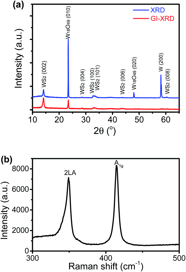 | ||
| Fig. 2 (a) XRD patterns of the S-containing nanosheet film detected in normal detection mode or grazing-incidence detection mode; (b) Raman spectrum. | ||
TEM-equipped EDS elemental mappings for W/S/O recorded on a nanosheet are shown in Fig. 3a, verifying the formation of WS2 with a small amount of oxygen being uniformly doped into the structure. The HRTEM observations identified the formation of WS2 nanosheets, as shown in Fig. 3b–e. A HRTEM image taken along the [001] projection is shown in Fig. 3b and its corresponding fast-Fourier transformation (FFT) pattern is shown in the inset, in agreement with the formation of the 2H phase of WS2. As shown in Fig. 3c–e, most nanosheets possess 1–4 layers with the (002) basal plane spacing at 0.63 nm, and most of the nanosheets are thinned down to only 1–2 layers near the edges.
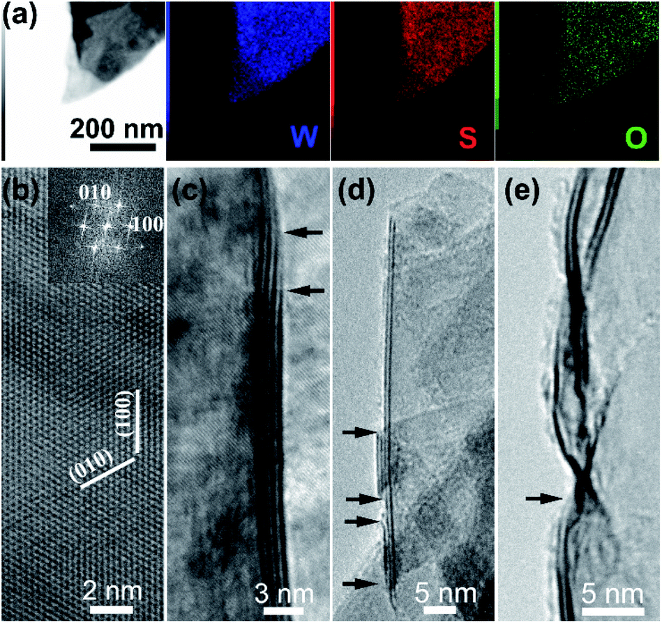 | ||
| Fig. 3 (a) EDS elemental mappings of a WS2 nanosheet; (b)–(e) representative high-resolution TEM images of WS2 nanosheets. | ||
The XRD spectra of the thin film grown with Se in normal detection mode or grazing-incidence detection mode are shown in Fig. 4a, indicating the formation of a hexagonal WSe2 phase (PDF#: 38-1388) along with monoclinic W18O49 (PDF#: 05-0392) and monoclinic WO2 (PDF#: 32-1393). It is worth noting that the peak of the WSe2 (002) basal plane peaked at 13.5°, a small shift from the 13.62° of the bulk, indicating a slight spacing increase between the (002) basal planes in the formed nanostructures. Similar to that observed with the WS2 thin film, in comparison between GIXRD and normal XRD of the same film, it can be seen that no peak from the W substrate was detected in GIXRD mode, and in the meantime the intensity from the WSe2 phase was stronger, suggesting the formation of a WSe2 phase on the surface, while the intensity of the two tungsten oxide phases was depressed, implying that two oxide phases are buried underneath surficial WSe2. The relative change in the intensity of the two oxide phases indicates that the layer growth sequence on the W substrate started with W18O49, next WO2, and finished with WSe2 nanosheets on top. Slightly different from the interfacial layer of WS2 nanosheets, the interfacial layer underneath the WSe2 nanosheets was composed of two phases, W18O49 and WO2. It is worth noting that both W18O49 and WO2 phases are highly conductive oxides for electric transport. The Raman spectrum of the nanostructures (Fig. 4b) exhibits a characteristic peak of the E2g1 mode at 248 cm−1 for WSe2, and its weakly detected B12g mode at 305 cm−1 indicates few-layer structures of the nanosheets.20 The XPS results also supported the formation of WSe2 nanostructures. The respective XPS spectra of W 4f and Se 3d are shown in Fig. 4c and d, revealing three peaks of W 4f, two with binding energies of 32.3 eV and 34.5 eV corresponding to the W4+ ionic state resulting from WSe2 and another one with a binding energy of 37.8 eV corresponding to the W6+ ionic state from the O-doping at the selenide defective sites. Two peaks of Se 3d were detected at 54.6 eV and 55.5 eV, respectively, which are consistent with the characteristics of 2H WSe2.16 The O-doping was further confirmed using EDS elemental mapping in TEM characterization. The presence of oxygen in the 2D nanosheets was due to the involvement of oxygen gas during high-temperature CVD growth of WS2 or WSe2 nanosheets. The slight O-doping would be beneficial to improve the conductivity of the TMD nanosheets and enhance their electrocatalytic activity.13 The above results demonstrate that the in situ O-doping naturally happened during the CVD growth of the nanosheets, which would partially account for the aforementioned excellent catalytic performances of the as-grown nanosheets.
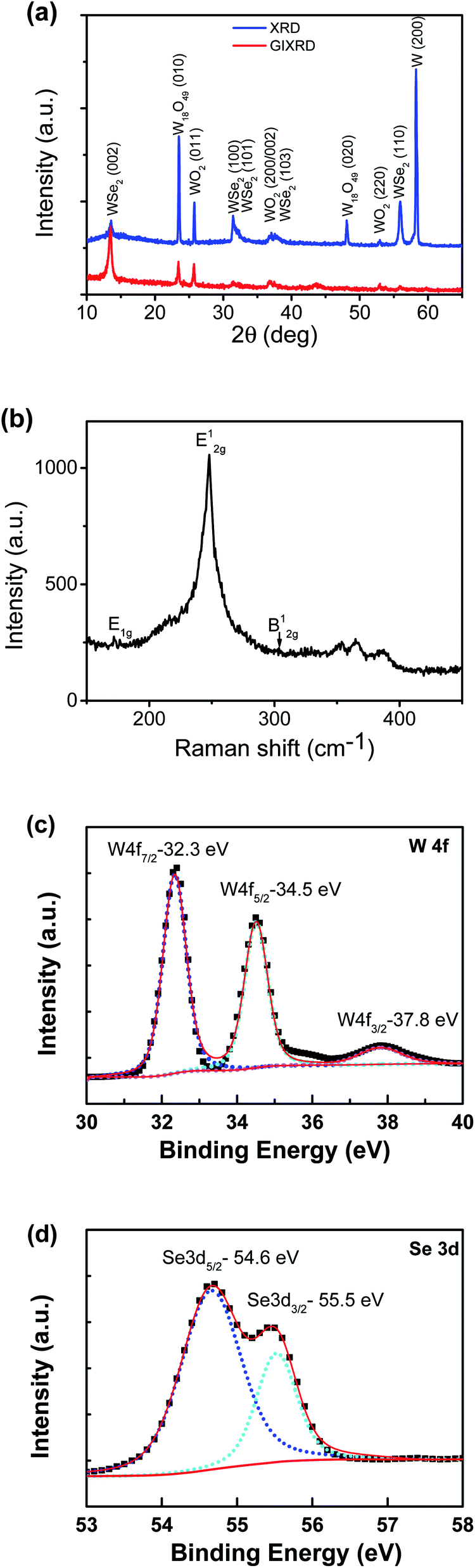 | ||
| Fig. 4 (a) XRD patterns of the Se-containing nanosheet thin film detected in normal detection mode or grazing-incidence detection mode. (b) Raman spectrum. (c) and (d) XPS spectra of W/Se. | ||
A low-magnification TEM image taken from some nano-barbules stemming from a feather-like nanosheet is displayed in Fig. 5a, showing their sharp tips. TEM-equipped EDS elemental mappings for W/Se/O recorded on the sharp tip of a nano-barbule are displayed in Fig. 5b, verifying the formation of WSe2 with a small amount of oxygen being doped into the structure, which is in agreement with the XPS results. The HRTEM observations identified the formation of WSe2 nanosheets, as shown in Fig. 5c–e. The sharp tips of the nanobarbules normally form either a 60° (Fig. 5c) or 30° (Fig. 5d) angle, resulting from their hexagonal packed crystal structure. Another common feature can be discerned from HRTEM images taken along the [001] projection in Fig. 5c and d, in which the characteristic periodic Moiré fringes show up. Moiré fringes can also be seen in Fig. 5a. This might be caused by small-angle rotations between the basal (002) plane layers due to the curved morphology of the nanosheets and weak van der Waals interlayer interactions in layered WSe2, similar to that observed on MoS2 3D nanoflowers.21 As shown in Fig. 5e, most nanosheets have few layers (1–4 layers) with the (002) basal plane spacing at 0.65 nm. The formation of the 2H phase was further verified through atomic resolution imaging (Fig. 5f). As shown in Fig. 5g, atomic resolution TEM observations also allowed us to confirm the formation of a metallic 1T phase.
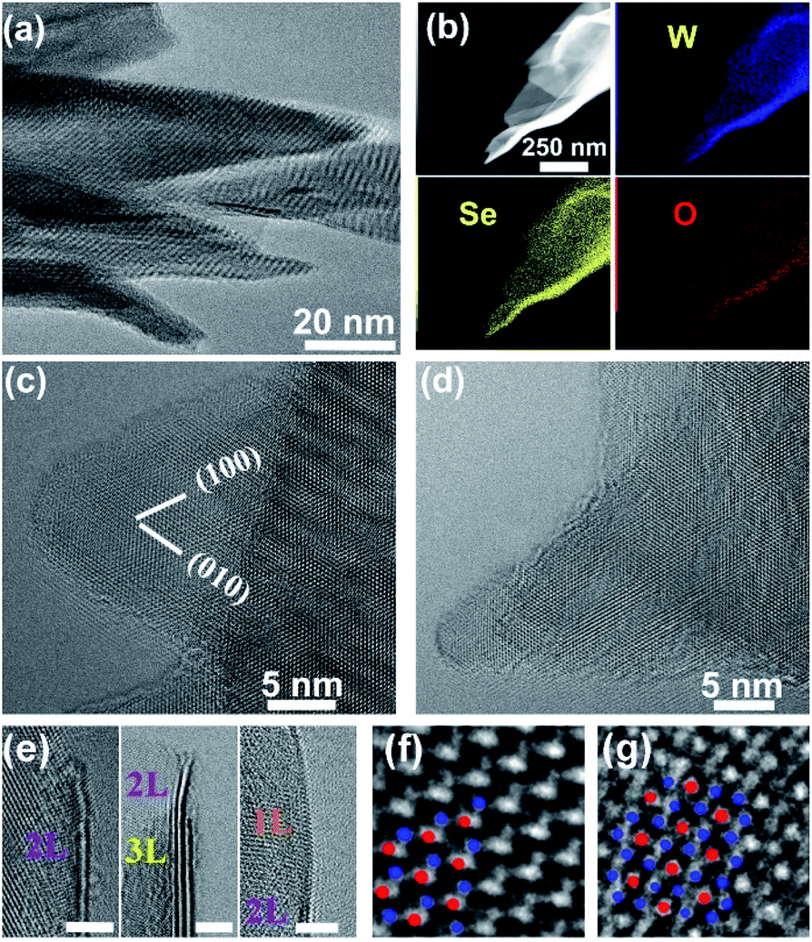 | ||
| Fig. 5 TEM characterization results of feather-like WSe2 nanosheets. (a) Low-magnification TEM image of nano-barbules of a feather-like nanosheet; (b) EDS elemental mappings for W/Se/O; (c)–(e) high-resolution TEM images of nano-barbules projecting from feather-like nanosheets; (f) atomic resolution image of the 2H phase, and (g) atomic resolution image of the 1T phase. W atoms are marked in red and Se atoms in blue. | ||
A vapor-solid process is presumed to control the formation of the nanostructures. Due to oxidation in low-pressure air, WOx is formed on the hot surface of the W target and continuously evaporated during the heating process. The W target can be quickly heated up to reach the setting temperature within a few seconds, and so at the beginning of heating, W18O49 vapor was rapidly generated and then deposited onto the W substrate. However, it took a little bit longer for Se/S powders (resulting from the CVD setup configuration) to reach a temperature above their corresponding melting points (112.8 °C for S and 217 °C for Se) when Se/S started to evaporate under a reaction chamber pressure of 1 Torr. As described in the Experimental Section, we applied the same weight amount of S/Se for the growth of WS2 and WSe2 nanosheets, and so the molar amount of S was roughly 2.5 times that of Se. In the early stage of S-containing CVD growth, the S vapor quickly reached its saturated state in which W18O49 vapor completely reacted with S vapor to form WS2 and deposited onto the W18O49/W substrate, while in Se-containing CVD growth it took longer for the Se vapor to reach a saturated state in which W18O49 vapor completely reacted with Se vapor to form WSe2, and thus in the early stage of CVD growth W18O49 vapor reacted with insufficient Se vapor to form WO2 and deposited onto the W18O49/W substrate. With the concentration of Se vapor ramping up, W18O49 vapor fully reacts with Se to form WSe2 and deposits onto the surface where feather-like WSe2 nanostructures nucleate and keep growing. How a small amount of the metastable 1T WSe2 phase is also formed along with the 2H phase in this high-temperature CVD process is not clear yet, but we would suggest that the fast cooling at the end of growth might have helped in preserving the metastable 1T phase along with the stable 2H phase in the nanosheets. The synthesis of 1T′ phase WSe2 has recently been proved possible, and the metallic 1T′ phase can significantly enhance its catalysis.22 The above-described results demonstrated that we have successfully prepared very thin WSe2 nanosheets with a large number of edge sites associated with their feather-like morphology, and the nanosheets are slightly in situ doped with oxygen and contain a metallic phase, all of which would benefit this nanostructured thin film for high-efficiency electrocatalysis.
Fig. 6a shows the LSV curves using a W-supported WS2 nanosheet thin film electrode, a feather-like WSe2 nanosheet electrode, and a Pt working electrode (as the control), respectively, with the real potentials applied to the catalysts being iR-corrected and the currents being normalized to their geometric areas to get the corresponding current densities. At high currents, the catalysts suffered from minor fluctuations due to a slow desorption process associated with the formation of some relatively big hydrogen gas bubbles. The uncompensated resistance R was 2.35 Ω for the WSe2 working electrode and 2.34 Ω for the WS2 working electrode, as determined by EIS measurements presented in Fig. 6b, revealing that the intermediate highly conductive tungsten oxide layer did not bring significant real resistance loads on tungsten dichalcogenide nanosheet working electrodes. It was reported by Chhowalla's group that TMD basal planes could also contribute to electrocatalytic activity of the HER if there was good electronic coupling between the substrate and the nanosheets,6 which indicates that a low-resistance contact between catalytic nanosheets and the substrate is crucial to reach the full potential of thin film catalysts. There is little difference between the resistance of WSe2 and that of WS2 thin films, and the catalysis contribution from the W substrate and tungsten oxide interfacial layers was considered to be negligible,18 and so the aforementioned clear difference in HER catalytic performances should mainly be attributed to the structural difference between the two thin films. The onset potential to drive a current at a density of 1 mA cm−2 was measured to be 55 mV for the WSe2 nanosheet electrode, while the WS2 nanosheet electrode's onset potential is 110 mV. The onset potential of a feather-like WSe2 catalyst is much lower than that of WSe2 nanoflowers supported on a graphene nanosheet.11 The measured η10 values are 37 mV, 141 mV and 220 mV for the Pt, WSe2 and WS2 working electrodes, respectively. In terms of theη10 value, a feather-like WSe2 electrocatalyst, though inferior to noble metal Pt, is significantly better than a WS2 nanosheet catalyst. In comparison, both WS2 nanosheets and WSe2 nanosheets are very thin, but in lateral sizes WSe2 nanosheets are smaller than WS2 nanosheets, plus, importantly, WSe2 nanosheets have numerous sharp edges resulting from the feather-like shape, and thus many more active edge sites are expected for WSe2 nanosheets. In addition, a feather-like WSe2 nanosheet thin film electrocatalyst has a much lower η10 than other reported MoS2-based nanostructured thin film catalysts,16,17 and, in terms of the η10 value, it is slightly better than the uncapped WS2 nanotube array thin film18 and the recently reported 1T phase or oxidized WSe2 powder catalysts13,14 and is also comparable to the best performing nanostructured TMD powder catalysts such as single-layer MoSSe nanodots8 or graphene-supported WS2 nanosheets.9 The corresponding Tafel plots are presented in Fig. 6c, showing a Tafel slope of 86 mV per decade for WSe2 nanosheets which is smaller than the slope of 109 mV per decade for WS2 nanosheets, indicating that the WSe2 nanosheet catalyst is better than theWS2 catalyst as per their catalytic efficiency. Three principal steps, including the Volmer reaction (discharge step) with a Tafel slope of 120 mV dec−1, the Heyrovsky reaction (desorption step) with a Tafel slope of 40 mV dec−1 and the Tafel reaction (combination step) with a Tafel slope of 30 mV/dec, have been proposed to account for the HER activity in acidic electrolyte.23 A medium value of the nanosheet catalysts implies that either the discharge–desorption or the discharge–combination mechanism is operative in the HER catalytic process. The Tafel slope of WSe2 nanosheets is comparable to the values reported for other nanostructured WSe2.10–13 In order to evaluate its stability at high currents, another crucial factor in the catalyst performances, two potentials versus RHE (−0.6/−0.7 V without iR compensation) were applied to the WSe2 working electrode, and the current–time behaviours were continuously recorded for 10 hours. The WS2 working electrode was also tested at a potential of −0.6 V versus RHE for comparison. Fig. 6d clearly shows good stabilities for both samples, and especially the WSe2 working electrode showed negligible (within 2%) fluctuations in current densities under heavy loads at 199 mA cm−2 and 246 mA cm−2 over a long period of time, proving its good durability in high current operations. Two-dimensional WSe2 possesses outstanding optoelectrical properties, and excellent photovoltaic performance was demonstrated on a WSe2 homojunction device built with mechanically exfoliated flakes,24 and so, based on the superior HER catalysis of the feather-like WSe2 nanosheet thin film, we expect that it would be possible to design an integrated system containing a pure WSe2-based solar cell and electrocatalytic devices to realize efficient and direct conversion from solar to green fuel hydrogen, like the photo-electrochemical devices demonstrated with perovskite materials.25
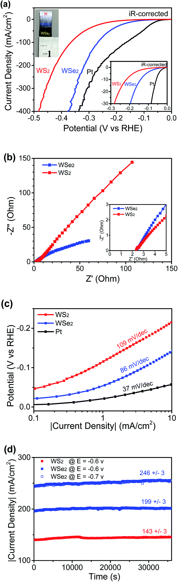 | ||
| Fig. 6 (a) LSV curves measured on working electrodes of WSe2 nanosheets, WS2 nanosheets, or Pt for the HER in acid. The inset shows a digital photo of a WSe2 thin film working electrode. (b) EIS Nyquist plots and (c) Tafel plots of different catalyst working electrodes. (d) Stability plots recorded on WSe2 thin film or WS2 thin film catalysts at different high-current levels. | ||
Conclusions
To sum up, feather-like WSe2 nanosheets were successfully synthesized using an infrared-heating CVD process, and proven to be an excellent electrocatalyst for the HER in acid because of its long-term stability at high currents, and a very low overpotential of 141 mV to drive a current density of 10 mA cm−2. Except the contribution from unique feather-like morphology to help maximize their active edge sites, the formation of a metallic 1T phase and the slight O-doping would increase the overall electrical conductivity of this thin film catalyst. Besides, it is known that both W18O49 and WO2 are highly conductive, and so the charge transfer between the W substrate and WSe2 nanosheets should have not been hindered much by the presence of interfacial oxide layers. Infrared-heating is a standard technique in semiconductor mass production process lines, and, as we demonstrated in our previous work,18 the infrared-heating CVD method employed in this work can easily be scaled up for large-area thin film growth, and so we could foresee practical application for feather-like WSe2 nanosheets in water splitting.Conflicts of interest
There are no conflicts to declare.Acknowledgements
Y.L. is thankful for the financial support from the Hundred Talents Plan of Hebei Province (E2018100001) and from Hebei University (521000981204).Notes and references
- X. Zou and Y. Zhan, Chem. Soc. Rev., 2015, 44, 5148 RSC.
- N. Han, K. Yang, Z. Lu, Y. Li, W. Xu, T. Gao, Z. Cai, Y. Zhang, V. S. Batista, W. Liu and X. Sun, Nat. Commun., 2018, 9, 924 CrossRef PubMed.
- J. Yang, A. R. Mohmad, Y. Wang, R. Fullon, X. Song, F. Zhao, I. Bozkurt, M. Augustin, E. J. G. Santos, H. S. Shin, W. Zhang, D. Voiry, H. Y. Jeong and M. Chhowalla, Nat. Mater., 2019, 18, 1309 CrossRef CAS PubMed.
- L. Lin, P. Sherrell, Y. Liu, W. Lei, S. Zhang, H. Zhang, G. G. Wallace and J. Chen, Adv. Energy Mater., 2020, 10, 1903870 CrossRef CAS.
- T. F. Jaramillo, K. P. Jørgensen, J. Bonde, J. H. Nielsen, S. Horch and I. Chorkendorff, Science, 2007, 317, 100 CrossRef CAS PubMed.
- D. Voiry, R. Fullon, J. Yang, C. Silva, R. Kappera, I. Bozkurt, D. Kaplan, M. J. Lagos, P. E. Batson, G. Gupta, A. D. Mohite, L. Dong, D. Er, V. B. Shenoy, T. Asefa and M. Chhowalla, Nat. Mater., 2016, 15, 1003 CrossRef CAS PubMed.
- C. Wei, R. R. Rao, J. Peng, B. Huang, I. E. L. Stephens, M. Risch, Z. J. Xu and Y. Shao-Horn, Adv. Mater., 2019, 31, 1806296 CrossRef PubMed.
- C. Tan, Z. Luo, A. Chaturvedi, Y. Cai, Y. Du, Y. Gong, Y. Huang, Z. Lai, X. Zhang, L. Zheng, X. Qi, M. Goh, J. Wang, S. Han, X. Wu, L. Gu, C. Kloc and H. Zhang, Adv. Mater., 2018, 30, 1705509 CrossRef PubMed.
- W. Han, Z. Liu, Y. Pan, G. Guo, J. Zou, Y. Xia, Z. Peng, W. Li and A. Dong, Adv. Mater., 2020, 32, 2002584 CrossRef CAS PubMed.
- D. A. Henckel, O. M. Lenz, K. M. Krishnan and B. M. Cossairt, Nano Lett., 2018, 18, 2329 CrossRef CAS PubMed.
- X. Wang, Y. Chen, B. Zheng, F. Qi, J. He, P. Li and W. Zhang, Electrochim. Acta, 2016, 222, 1293 CrossRef CAS.
- X. Wang, Y. Chen, F. Qi, B. Zheng, J. He, Q. Li, P. Li, W. Zhang and Y. Li, Electrochem. Commun., 2016, 72, 74 CrossRef CAS.
- P. M. Pataniya, X. Yang, B. Li, D. Kannichankandy and C. K. Sumesh, Int. J. Energy Res., 2022, 1–9, DOI:10.1002/er.7971.
- M. Muska, Y. Wang, J. Yang, L. Ma, Q. Xu, H. Ding, J. Zhu and Q. Yang, ACS Appl. Nano Mater., 2022, 5, 6410 CrossRef CAS.
- J. M. Velazquez, F. H. Saadi, A. P. Pieterick, J. M. Spurgeon, M. P. Soriaga, B. S. Brunschwig and N. S. Lewis, J. Electroanal. Chem., 2014, 716, 45 CrossRef CAS.
- J. Kibsgaard, Z. Chen, B. N. Reinecke and T. F. Jaramillo, Nat. Mater., 2012, 11, 963 CrossRef CAS PubMed.
- Y. Yang, H. Fei, G. Ruan, C. Xiang and J. M. Tour, Adv. Mater., 2014, 26, 8163 CrossRef CAS PubMed.
- Y. Li, W. Zhang, T. Wang, Y. Cao, C. Lv and K. Zhang, Nanoscale Adv., 2021, 3, 6587–6595 RSC.
- A. Berkdemir, H. R. Gutierrez, A. R. Botello-Mendez, N. Perea-Lopez, A. L. Elías, C. I. Chia, B. Wang, V. H. Crespi, F. Lopez-Urias, J. C. Charlier, H. Terrones and M. Terrones, Sci. Rep., 2013, 3, 1755 CrossRef.
- J. K. Huang, J. Pu, C. L. Hsu, M. H. Chiu, Z. Y. Juang, Y. H. Chang, W. H. Chang, Y. Iwasa, T. Takenobu and L. J. Li, ACS Nano, 2014, 8, 923 CrossRef CAS PubMed.
- Y. Li, Y. Bando and D. Golberg, Appl. Phys. Lett., 2003, 82, 1962 CrossRef CAS.
- M. S. Sokolikova, P. C. Sherrell, P. Palczynski, V. L. Bemmer and C. Mattevi, Nat. Commun., 2019, 10, 712 CrossRef CAS PubMed.
- L. A. Kibler, ChemPhysChem, 2006, 7, 985 CrossRef CAS PubMed.
- Y. Zhang, K. Ma, C. Zhao, W. Hong, C. Nie, Z. Qiu and S. Wang, ACS Nano, 2021, 15, 4405 CrossRef CAS PubMed.
- H. Zhang, Y. Lu, W. Han, J. Zhu, Y. Zhang and W. Huang, Chem. Eng. J., 2020, 393, 124766 CrossRef CAS.
| This journal is © The Royal Society of Chemistry 2022 |